Note: Descriptions are shown in the official language in which they were submitted.
CA 02297129 2001-05-29
-1-
METHOD AND APPARATUS FOR RECOVERY OF TIME SKEWED DATA ON A
PARALLEL BUS
Field Of The Invention
The invention relates to the recovery of parallel data by a receiving device,
and more
particularly to the recovery of time-skewed parallel data from a backplane bus
such that it can be
further processed within a synchronous clock domain.
Background Of The Invention
1o It is well known in the art of digital data transfer that high data rates
can be achieved by
transferring data over a parallel data bus. For a given bus rate, the bus
bandwidth measured in
bits-per-second is equivalent to the bus rate times the number of data signals
comprising the
parallel data bus.
A typical system might include a number of modules which interface to a
backplane
1 s module. The modules intercommunicate via a parallel bus on the backplane
module. A
transmitting module transmits data over the backplane bus synchronous with a
clock on the
transmitting module; thus, all transitions on all signal lines on the
backplane bus leave the
transmitting module in a synchronous relationship to the clock on the
transmitting module.
Receiving modules also implement a clock at the bus rate, and receive the data
on the backplane
2o bus synchronous to the receive clock.
In such prior art systems, it is necessary to ensure that the receive clocks
have a specific
phase relationship to the transmit clock. to ensure proper data recovery. For
example, the
transmit clock may be transmitted to the receiving modules over the backplane,
the receive
clocks then being derived from it.
2s In any system where a parallel bus is implemented on a backplane module,
there will be
some amount of time skew between the bus signals themselves and between the
bus signals and
the receive clock at the destination, since the signals are subject to
transmission delays due to
capacitive loading and line lengths. In low speed systems, this time skew is a
small percentage
of the overall clock period; thus, as long as the receive clock is in phase
with the transmit clock,
3o the skew does not interfere with data recovery and can therefore be
ignored.
Parallel buses, however, reach certain limitations as clock rates are
increased. In
particular, where a high-speed parallel bus is implemented on a backplane
module such that the
various signals making up the parallel bus must travel a significant distance
between their source
CA 02297129 2001-05-29
-2-
and destination, transmission delays on the data signals due to loading
variations and line
lengths cause relatively large time skews between the signals themselves and
between the
signals and receive clocks. As these time skews become a significant
percentage of the clock
frequency, they can non longer be ignored. Such time skews can preclude direct
use of the
receive clock for clocking the bus signals into a receive register or latch,
since setup and/or hold
time violations might occur, causing faulty data reception. The skew problem
becomes more
pronounced at higher clock rates, because as clock rates increase, data
signals need travel only a
short distance before these difficulties are encountered.
Prior art solutions to the skew problem typically center on minimizing the bus
skew seen
t o at the receiving module, through implementation, for example, of expensive
backplane module
manufacturing techniques employing impedance matching of the data lines
constituting the
parallel bus, or by minimizing the allowable length of the parallel bus. As
bus clock rates have
continued to increase, the expense and limitations of these prior solutions
have become
unacceptable.
Summary Of The Invention
In accordance with the principles of the invention there is provided an
apparatus and
method for receiving time skewed data from a parallel data bus. A data
transfer on the parallel
data bus is preceded by a start-of cell delimiter consisting of a
predetermined sequence of pulses
on each of the data signals. The data is received from the bus by receive
logic employing a local
clock.
Sampling logic is used to sample each of the data signals received from the
bus at a rate
which is higher than the local clock rate. A plurality of sample registers are
provided, each
sample register corresponding to one of the bus data signals. Each sample
register stores a
plurality of samples of the corresponding data signal, the number of samples
stored being large
enough to store at least some of the pulses constituting the start-of cell
delimiter. The samples
are output synchronous with the local clock. Start-of cell detect and center
select logic is used
for determining that a start-of cell delimiter is stored in each of the sample
registers, and for
determining which of the samples stored in each of the sample registers
represent the
3o approximate center sample of one of the pulses of the start-of cell
delimiter. These center
samples correspond to the data signals on the bus, but are de-skewed and
synchronous with the
local clock.
CA 02297129 2001-05-29
-3-
In accordance with a further aspect of the invention, parallel data can be
recovered even
when there is more than one bit time of skew between the data signals and the
local clock.
Accordingly, a delay register accepts the center samples provided by the
center selection logic
and provides as output a plurality of delayed signals, each delayed signal
corresponding to one
of the data signals on the bus. Delay logic is used to determine that some of
the start-of cell
delimiters were stored in the sample register a local clock cycle later than
the remaining start-of
cell delimiters. The delay logic produces as output the delayed center samples
corresponding to
the data signals for which a start-of cell delimiter was stored a local clock
cycle prior to the
other start-of cell delimiters, and produces as output the center samples
corresponding to the
to other data signals.
The present invention thereby provides a significant advance in the art of
parallel data
reception, in that received data can be properly processed despite relatively
large time skews
between the data signals and the local clock. The inventive concepts herein
disclosed thereby
allow implementation of longer parallel bus lengths using relatively
inexpensive module
manufacturing techniques to transfer parallel data at higher data transfer
rates than previously
possible.
Brief Description Of The Drawings
Figure 1 is a block diagram of a network switch employing the deskew logic of
the
present invention;
Figure 2 is a timing diagram depicting a data transfer on the backplane bus
shown in
Figure 1;
Figure 3 is a block diagram of the deskew logic shown in Figure l;
Figure 4 is a timing diagram of the clock generation logic shown in Figure 3;
Figure 5 is a block diagram of one of the bit recovery registers shown in
Figure 3;
Figure 6 represents the possible contents of one of the sample registers of
Figure 3 when
it stores a start-of cell delimiter;
Figure 7 is a block diagram of the start-of cell detect and center select
logic shown in
Figure 3;
3o Figure 8a-d are a flow diagram representing the operation of the start-of
cell detect and
center select logic shown in Figure 6;
Figure 9 is a block diagram of the control logic shown in Figure 3;
CA 02297129 2001-05-29
-4-
Figure 10 is a flow diagram of the EOC FSM shown in Figure 8;
Figure 11 is a flow diagram representing the operation of the control FSM
shown in
Figure 8;
Figure 12 is a block diagram of the deskew logic showing additional components
to
correct for bus skew of greater than one bit time;
Figure 13 is a flow diagram of the control logic as shown in Figure 11, as
modified to
correct for bus skew of greater than one bit time; and
Figure 14 is a flow diagram of the data delay FSM as shown in Figure 11.
Detailed Description Of The Preferred Embodiment
1o Referring now to Figure l, there is shown a network switch which
incorporates the
present invention. A network switch chassis 10 has installed within it a
number of switching
modules 12. The switching modules 12 are interconnected via backplane bus 14.
Each of nodes
16, 18, 20, 22, 24, and 26 is connected to one of the switching modules 12. In
the event that, for
example, node 16 communicates with node 18, a data transfer between the nodes
is switched
15 through the switching module 12 to which the two nodes are connected.
However, if node 16
communicates with node 20, then the data transfer between these two nodes
utilizes the
backplane bus 14.
Each of the switching modules 12 includes a bus interface 28 coupled to the
backplane
bus 14. A l OMhz clock signal 30 is distributed amongst the switching modules
12 via the
2o backplane bus 14. Within each bus interface 28 there is included clock
generation logic 32
which uses the lOMhz clock signal received from the backplane bus 14 to
generate a SOMhz
local clock signal 36 for use by the bus interface 28. The bus interface 28
contains transmit
logic 38 for transmitting data on the backplane bus 14 in synchronism with the
local clock signal
36, and receive logic 40 for receiving data from the backplane bus 14. Data
received from the
25 backplane bus 14 is processed through deskew logic 42, and is then
forwarded in synchronism
with the local clock signal 36 for further processing by the switching module
12.
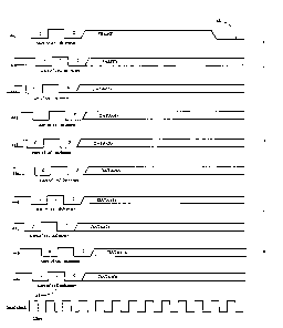
Data is transferred over the backplane bus 14 in a bytewise parallel manner as
shown in
Figure 2. The backplane bus 14 contains 10 separate bus signals 44:
backplane_data<7:0>
signals 44a-h, a backplane_parity signal 44i, and a backplane_frame signal
44j. The backplane
30 bus rate as herein embodied is SOMhz - that is, a byte of data is
transferred every 20ns.
Individual data transfers from a given switching module 12 over the backplane
bus 14 are
CA 02297129 2001-05-29
- S -
differentiated by a start-of cell delimiter 45 and an end-of cell indicator
46. A data transfer
begins with a start-of cell delimiter 45 which is asserted on each of the bus
signals 44, herein
shown as a three bit sequence consisting of a binary '0 followed by a '1
followed by a '0 .
The backplane_frame signal 44j is then asserted, indicating that a valid data
transfer is
s occurring. A variable number of bytes of data are then transferred in a
bytewise parallel manner
via the backplane_data<7:0> signals and the backplane_parity signal. The
backplane_frame
signal 44j is deasserted just prior to the last two bytes of data transferred
over the
backplane_data<7:0> and backplane_parity signals. The deassertion of the
backplane_frame
signal 44j serves as the end-of cell indicator 46.
1o The bus signals 44 making up the data transfer are depicted in the Figure
as they might
arrive at a receiving switching module 12. As seen, though each of the
backplane_data<7:0>,
backplane_parity, and backplane_frame signals 44 making up the data transfer
are transmitted
by a given switching module 12 in synchronism with the transmitting module's
local clock
signal 36, the backplane_data<7:0>, backplane_parity, and backplane_frame
signals may not
15 necessarily arrive at the receiving switching module 12 in the same phase
relationship with each
other and with the receiving switching module 12 local clock signal 36.
Rather, the bits can
arnve in a time skewed relationship to each other and to the local clock
signal 36 due to
differences in the transmission delays for each signal over the backplane bus
14. As seen for
instance on the backplane_data<1> signal, the skew between the bus signal 44c
and the local
2o clock 36 can be up to 20ns or 1 bit time. Such skews preclude the use of
the local clock 36 for
clocking the bus signals 44 into a receive register or latch, since setup
and/or hold time
violations might occur, causing faulty data reception. Each switching module's
bus interface 28
therefore contains the deskew logic 42 to compensate for skew between the
various bus signals
44 making up the backplane bus 14 and the receiving switching module's local
clock 36.
2s Referring now to Figure 3, there is shown the deskew logic 42 for a given
switching
module 12. The major components of the deskew logic 42 include a data recovery
register 48
and recovery logic 50. These components intemperate to deskew the backplane
bus signals
relative to the SOMhz local clock generally as follows: the clock generation
logic 32 is used to
produce sample clock signals 53 for high-speed sampling of each of the
backplane bus signals
30 44. The sample clock signals 53 allow sampling of the backplane bus signals
44 at a rate greater
than SOMhz bus rate. The sample clocks 53 are used to clock data into the data
recovery register
48. The data recovery register 48 includes bit recovery registers 54, one for
each of the
CA 02297129 2001-05-29
-6-
backplane bus signals 44. Each bit recovery register 48 includes sampling
logic 55, which uses
the sample clocks 53 to sample the corresponding backplane bus signal 44. The
sampling logic
55 feeds a sample register 56, which stores a number of samples sufficient to
store an entire
instance of the start-of cell delimiter 45 for a given bus signal 44. These
samples are output
from the sample register 56 synchronous with the local clock signal. The
recovery logic 50 is
used to determine that each sample register 56 presently stores a start-of
cell delimiter 45. The
recovery logic 50 then analyzes one of the stored pulses constituting the
start-of cell delimiter to
determine which of the samples stored in the sample register 56 represents the
approximate
center sample of the pulse. The location in the sample register 56 which
stores this center
1o sample represents the corresponding recovered deskewed backplane bus signal
44 synchronous
with the local clock, and is used as such by the switching module 12 for the
duration of the data
transfer.
The various components comprising the deskew logic 42 are now described in
further
detail. The clock generation 32 operates to provide sample clocks 53 as shown
in Figure 4. The
clock generation logic 32 receives the lOMhz system clock 30 and multiplies it
via the PLL 34
to 150Mhz, which is then divided down by divide-down logic 57 to six SOMhz
clocks in various
phase relationships. As shown, the CLK150 signal is divided down to provide
the SOMhz local
clock 36 and SOMhz sample clock signals 53 of various phases: sample c1k50<0>,
sample c1k50<1>, sample c1k50<2>, sample c1k50<3>, sample c1k50<4>, sample
c1k50<5>,
2o sample c1k50<6>, and the local clock 36. The divide-down logic 57 which
produces these
signals may do so in any number of ways well known in the art.
Note that, between the rising edges of the local clock signal, the rising
edges of the
various sample clk<5:0> signals provide 6 different sampling points. For each
of bus signals 44
making up the backplane bus 14, the sample clk<5:0> signals are used by the
sampling logic 55
to sample each of the bus signals 44 between local clock 36 edges. The various
samples are
later used by the recovery logic 50 to compensate for skew between each of the
bus signals 44
and the local clock signal 36. Though the preferred embodiment implements six
times
oversampling, it will be understood by one skilled in the art that a greater
or fewer number of
samples could be effectively employed, the minimum sampling rate being
dependent upon the
3o signalling characteristics of the backplane bus.
As seen in Figure 3, the data recovery register 48 includes 10 bit recovery
registers 54,
one coupled to each of the bus signals 44. Referring now to Figure S, there is
shown in detail
one of the bit recovery registers 54. The bit recovery register 54 contains 7
stages. The timing
CA 02297129 2001-05-29
relationships between these stages is shown in Figure 4. Stage 1, which makes
up the sampling
logic S5, contains bit registers 60 - 82, each of which may be for example a D
flip-flop. The
inputs of each of the bit registers 60 - 70 are fed by a single one of the
backplane bus signals 44
making up the backplane bus 14. In the figure, the bit recovery register 54
receives the
backplane_data<0> signal. Bit registers 60 and 72 are clocked by sample
clk<0>, and form a
dual-rank synchronizer. Similarly, bit registers 62 and 74 are clocked by
sample clk<1>, bit
registers 64 and 76 are clocked by sample clk<2>, bit registers 66 and 78 are
clocked by
sample clk<3>, bit registers 68 and 80 are clocked by sample clk<4>, and bit
registers 70 and
82 are clocked by sample clk<5>. Thus, at the output of the sampling logic 58
there are
1o provided 6 different samples of the backplane_data<0> signal.
It should be noted that, though the sampling logic described with reference to
the
preferred embodiment utilizes several SOMhz clocks of differing phases in
order to capture six
different samples of a backplane_data signal 44 during a local clock cycle,
alternate
arrangements exist to sample the data at a rate higher than the local clock
rate. For instance, a
single higher rate clock signal could be used, with the stage 1 logic arranged
as a serial register
clocked by the single higher rate clock.
Stage 2 clocks the first 3 samples of the backplane_data<0> signal into bit
registers 84,
86, and 88, while stage 3 clocks the other 3 samples of the backplane_data<0>
signal into bit
registers 90, 92, and 94. The registers 84, 86, and 88 of stage 2 are clocked
by sample clk<6>,
2o while the registers 90, 92, and 94 of stage 3 are clocked by the local
clock 36. The stage 2 and
stage 3 registers are clocked by different clocks in order to optimize the
setup and hold times of
the input data signals to the respective clock edge. As seen in Figure 2, the
rising edge of the
local clock signal can easily be used to clock data which was stored on the
rising edges of
sample clks<3:5>, but the rising edge of the local clock signal and sample
clk<1> are so close
together as to potentially cause a setup time violation on bit register 86.
Sample clk<6>,
however, has an optimal timing relationship to data clocked off of the sample
clk<0:2> edges,
and is thus used to clock stage 2. It should be noted that the invention is
not limited; that is, the
stage 2 and stage 3 registers are shown clocked in a manner that is specific
to the
implementation shown. For instance, in implementations using sample clock
signals with
3o different timing relationships relative to the local clock signal, it may
be possible to combine
stages 2 and 3 to be clocked by the local clock, or to eliminate stages 2 and
3.
Stages 4 through 7 make up the 19 bit sample register 56. Stage 4 clocks the
first 6
CA 02297129 2001-05-29
_ 8 -
samples of the backplane_data<0> signal into sample bit registers 98 - 108
synchronous with the
local clock. On the next local clock edge, these samples are clocked into the
bit registers 110 -
120 making up stage 5, while the next 6 samples of the backplane_data<0>
signal are clocked
into stage 4. On the following local clock edge, these samples are clocked
into the sample bit
registers 122 - 132 making up stag 6, and finally, on the next local clock
edge, into the sample
bit register 134 making up stage 7. The sample register 56 now contains 19
samples of the
backplane_data<0> signal taken over 4 local clock edges.
The contents of the sample register 56 is used by the recovery logic 50 to
detect start-of
cell delimiters 45 and to determine the center sample of one of the pulses of
the start-of cell
1 o delimiter, thereby providing optimally sampled data for use by the
switching module 12. In
Figure 3, the recovery logic is shown to include 10 instances of start-of cell
detect and center
select logic 136, each fed by one of the sample registers 56. Each instance of
the start-of cell
detect and center select logic 136 is coupled to control logic 138. Each
instance of the start-of
cell detect and center select logic 136 produces an SC detect signal 140. The
SC detect
signals<9:0> are fed the control logic 138, which feeds back SC error and EOC
signals 142 and
144 to each instance of the start-of cell detect and center select logic 136.
The recovery logic 50 operates generally as follows. Each instance of the
start-of cell
detection and center selection logic 136 monitors the contents of the
corresponding sample
register for the presence of a start-of cell delimiter 45. When a valid start-
of cell delimiter 45 is
2o detected, the start-of cell detect and center select logic asserts its SC
detect signal, and
determines which of the sample bit registers 98 - 134 holds the approximate
center sample of the
logic '1 pulse in the start-of cell delimiter. The bit register holding this
center sample is then
provided as an output center data signal, which is a de-skewed and
synchronized version of the
corresponding backplane_data signal, for the duration of the data transfer.
The control logic 138
monitors the SC detect<9:0> signals to determine whether a start-of cell
delimiter has been
detected on all backplane bus signals 44 within a single local clock 36
period. If so, the
data valid bit is asserted. If, however, a start-of cell delimiter has not
been detected on one or
more backplane bus signals within a single local clock period, then either
there is a general bus
error, or the bus skew exceeds a bit time on at least one of the bus signals
44. The SC error
3o signal is then asserted, indicating a start-of cell error. In either case,
the control logic 138 awaits
the end of the data transfer. When the end of the data transfer is detected,
the control logic 138
asserts the EOC signal, thereby resetting each instance of the start-of cell
detect and center select
CA 02297129 2001-05-29
-9-
logic 136 to detect the next start-of cell delimiter 45.
The start-of cell detect and center select logic 136 should indicate detection
of a valid
start-of cell delimiter 45 while rejecting incorrect sequences. In the present
embodiment, a start-
s of cell delimiter 45 consists of a logic '0 followed by a logic ' 1 followed
by a logic '0 (see
Fig. 3_. Thus, the start-of cell detect and center select logic 136 should
detect a '010
sequence as a valid start-of cell delimiter, while rejecting sequences such as
'011 or '1110 .
Due to bus skew and delay differences which can result in an uneven duty cycle
on a given bus
signal line, valid logic levels may be anywhere between 2 and 8 samples long.
In addition, noise
l0 may result in a logic '0 or ' 1 pulse that can be detected for a single
sample. Thus, the start-
of cell detect and center select logic 136 as embodied herein requires that a
start-of cell '1
pulse and trailing '0 pulse be at least a minimum width (or number of
samples), and that a
start-of cell ' 1 pulse not exceed a maximum width (number of samples), and
that the start-of
cell leading '0' pulse be a minimum width (number of samples). Based on the
implemented
15 sampling rate of 300Mhz (6 samples per SOMhz clock period), the start-of
cell detect and center
select logic 136 requires the following sequence: a leading logic '0' of
minimum duration 2
samples, followed by logic '1' of minimum duration 4 samples and maximum
duration 8
samples, followed by a logic '0' of minimum duration 4 samples. Thus, since 14
bits are
required to store a valid sample, and that sample may be captured on any of 6
different
2o sample clk edges, the sample register 56 contains 19 sample bit registers
98 - 134, as shown in
Figure 4. It should be noted, however, that in alternative implementations,
data transfers might
be preceded by relatively long start-of cell delimiters. In this case, it may
be sufficient to store
only a portion of the start-of cell delimiter in order to properly determine
that a delimiter has
been captured and to determine the center sample of one of the pulses in the
delimiter.
25 In Figure 6 there is shown the possible contents of one of the sample
registers 56
containing a valid start-of cell delimiter 45. Starting from a given one of
six sample points, there
will exist two '0' samples, followed later by four '1' samples, followed later
by four '0' samples.
The remaining samples are considered "don't cares", and are marked herein with
an 'x'. The
start-of cell detect and center select logic 136 uses the contents of the
sample register 56 to
3o determine the presence of a start-of cell delimiter 45 and to determine
which of the bit registers
98 - 134 within the sample register 56 stores the sample which is closest to
the center of the '1'
pulse within the start-of cell delimiter 45. The center of the sampled '1'
pulse will be chosen
somewhere between b6 (the output of the sample bit register 110 and b12 (the
output of the
CA 02297129 2001-05-29
- 10-
sample bit register 122). The output of this chosen sample bit register will
then be selected for
use as the de-skewed and synchronized version of the corresponding backplane
bus signal 44 for
the duration of the data transfer.
The operation of an instance of the start-of cell detect and center select
logic 136 is now
described in detail with reference to Figures 7 and 8a-d. In Figure 7 there is
shown the instance
of the start-of cell detect and center select logic 136 corresponding to the
backplane_data<0>
signal. The start-of cell detect and center select logic 136 includes center
select logic 150 which
receives the outputs b0 - b18 of the sample register 56 corresponding to the
backplane_data<0>
signal 44a, as well as the EOC and SC error signals 144 and 142 from the
control logic 138.
1o The center select logic 136 produces as output the SC detect<0> signal 140,
and select signals
sel<2:0>. The sel<2:0> signals feed the control inputs of a multiplexes 152.
The sel<2:0>
signals select one of the sample register 56 outputs b<12:6> or a logic 0 to
drive the multiplexes
output signal center data<0>.
Referring now to Figures 8a-d, there is shown the process undertaken by the
start-of cell
detect and center select logic 136 to identify the start-of cell delimiter 45
and the center of the '1'
pulse for the bus signal backplane_data<0>. Upon reset (step 151), the SC
detect<0> signal is
deasserted and the sel<2:0> outputs are set to a logic '0' (step 152). If the
EOC and SC error
signals are deasserted (steps 154 and 156), and if the SC detect<0> signal has
not yet been
asserted (step 158), then the contents of the sample register 56 is masked
(logically Aanded@)
2o with a mask value of Ox30ff, thus allowing the data samples at bit
locations b13, b12, and b7 - b0
to be examined for a valid start-of cell delimiter 45. The result of the
masking function is then
compared to the value 'OxfI7' (step 160). A match indicates that locations b
13 and b 12 contain a
logic 0 and therefore a valid leading '0', and that locations b7 - b4 contain
a logic ' 1' and
therefore indicate a valid '1' pulse, and that locations b3 - b0 contain a
logic '0' and therefore
indicate a valid trailing '0' pulse. The SC detect<0> signal is then asserted
(step 162). The
sample register 56 contents is then masked with the value 0x3000, and compared
with the value
0x300 (step 164). A match indicates that bits b9 and b8 contain a logic '1'
and that the center '1'
pulse is at least 6 samples long. In this case, the center of the '1' pulse is
chosen at b7 (step 166).
The sel<2:0> signals are driven with a value of '010' to select the third
input to the multiplexes
152, thereby driving the b7 signal from the sample register 56 onto the output
center data<0>
signal. On the other hand, no match indicates that the '1' pulse is no greater
than 5 samples long.
The center of the ' 1' pulse in this case is chosen at b6 (step 168). The
sel<2:0> signals are in this
CA 02297129 2001-05-29
-11-
case driven with a value of '001' to select the second input to the
multiplexer 152, thereby driving
the b6 signal from the sample register 56 onto the output center data<0>
signal. After a center bit
is selected, the center select logic 150 returns to step 154. Since the SC
detect<0> signal is now
asserted (step 158), the logic awaits either the assertion of the EOC signal,
indicating the end of
s the current data transfer (step 154), or the assertion of the SC error
signal (step 156). Upon the
assertion of either signal, the logic resets the SC detect<0> signal and the
sel<2:0> signals (step
152) and the process is repeated.
In the event that the mask comparison at step 160 failed, the contents of the
sample
register 56 is instead masked with a value 'Ox6lfe' to examine the data
samples at bit locations
1 o b 14, b 13, and b8 - b 1 for a valid start-of cell delimiter. The result
of the masking function is
compared with a value OxleO (step 170). A match, as above, indicates a valid
start-of cell
delimiter and therefore the SC detect<0> signal is asserted (step 172). The
contents of the
sample register 56 is then compared with a value 0x600 in order to determine
the width of the
' 1' pulse (step 174). A match indicates that bits b 10 and b9 contain a logic
' 1' and that the
15 center '1' pulse is at least 6 samples long. In this case, the center of
the '1' pulse is chosen at b8
(step 176). The sel<2:0> signals are driven with a value of '011' to select
the fourth input to the
multiplexer 152, thereby driving the b8 signal from the sample register 56
onto the output
center data<0> signal. No match indicates that the '1' pulse is no greater
than 5 samples long.
The center of the '1' pulse in this case is chosen at b7 (step 178). The
sel<2:0> signals are then
20 driven with a value of '010' to select the third input to the multiplexer
152, thereby driving the
b7 signal from the sample register 56 onto the output center data<0> signal.
This comparison process is repeated for the remaining possible sample register
56
contents in the same manner. If the mask comparison at step 170 failed, then a
mask value of
Oxc3fc is used (step 180) and compared to a value of Ox3c0. A match indicates
a valid start-of
25 cell delimiter, and the SC detect<0> signal is asserted (step 182). A mask
of Oxc00 is then
applied to determine whether the center of the '1' pulse is at b9 or b8 (step
184). If the center of
the '1' pulse is at b9, the sel<2:0> lines are driven with a value of '100' to
select the fifth input
to the multiplexer 152, thereby driving the b9 signal from the sample register
56 onto the output
center data<0> signal. If the center of the ' 1' pulse is at b8, the sel<2:0>
lines are driven with a
3o value of '011' to select the fourth input to the multiplexer 152, thereby
driving the b8 signal
from the sample register 56 onto the output center data<0> signal.
If the mask comparison at step 180 failed, then a mask value of Ox187f8 is
used (step
CA 02297129 2001-05-29
- 12-
190) and compared to a value of 0x780. A match indicates a valid start-of cell
delimiter. The
SC detect<0> signal is then asserted (step 192). A mask of 0x1800 is then
applied to determine
whether the center of the '1' pulse is at b10 or b9 (step 194). If the center
of the '1' pulse is at
b10, the sel<2:0> lines are driven with a value of '101' to select the sixth
input to the
multiplexer 152, thereby driving the b10 signal from the sample register 56
onto the output
center data<0> signal. If the center of the '1' pulse is at b9, the sel<2:0>
lines are driven with a
value of ' 100' to select the fifth input to the multiplexer 152, thereby
driving the b9 signal from
the sample register 56 onto the output center data<0> signal.
If the mask comparison at step 190 failed, then a mask value of Ox30ff~ is
used (step
l0 200) and compared to a value of Oxf00. A match indicates a valid start-of
cell delimiter, and the
SC detect<0> signal is asserted (step 202). A mask of 03000 is then applied to
determine
whether the center of the '1' pulse is at b1 l or b10 (step 204). If the
center of the '1' pulse is at
b1 l, the sel<2:0> lines are driven with a value of '110' to select the
seventh input to the
multiplexer 152, thereby driving the b 11 signal from the sample register 56
onto the output
center data<0> signal. If the center of the '1' pulse is at b10, the sel<2:0>
lines are driven with
a value of '101' to select the sixth input to the multiplexer 152, thereby
driving the b10 signal
from the sample register 56 onto the output center data<0> signal.
Finally, if the mask comparison at step 200 failed, then a mask value of 0x61
fe0 is used
(step 210) and compared to a value of Oxle00. A match indicates a valid start-
of cell delimiter,
2o and the SC detect<0> signal is asserted (step 212). A mask of 06000 is then
applied to
determine whether the center of the ' 1' pulse is then applied to determine
whether the center of
the '1' pulse is at b12 or b1 1 (step 214). If the center of the '1' pulse is
at b12, the sel<2:0>
lines are driven with a value of '111' to select the eighth input to the
multiplexer 152, thereby
driving the b12 signal from the sample register 56 onto the output center
data<0> signal. If the
center of the ' 1' pulse is at b 11, the sel<2:0> lines are driven with a
value of ' 110' to select the
seventh input to the multiplexer 152, thereby driving the b1 l signal from the
sample register 56
onto the output center data<0> signal.
If all of the above comparisons fail, then no start-of cell delimiter is
present. In this case,
the SC detect<0> signal remains deasserted, and the sel<2:0> signals remain
driven to a value
of '000', thereby driving a logic '0' level onto the center data<0> signal.
Referring back to Figure 3, each instance of start-of cell detect and center
select logic 136
provides as output on one of lines center data<frame>, center data<parity>, or
center data<7:0>
CA 02297129 2001-05-29
-13-
the contents of the sample register bit in the corresponding sample register
56 which represents
the approximate center sample of the ' 1' pulse in the start-of cell delimiter
45 for the
corresponding backplane_data signal. The lines center data<frame>, center
data<parity>, and
center data<7:0> lines are used by the switch module as the de-skewed and
synchronized
versions of the corresponding backplane bus signals 44 for the duration of the
data transfer.
Meanwhile, the control logic 138 monitors the SC detect<9:0> signals and the
center data<frame> signal to 1) check for bus errors and 2) determine the end
of the data
transfer in order to reset the start-of cell detect and center select logic
136. The control logic
138 is shown in further detail in Figure 9. The SC detect<9:0> signals are fed
to an AND
1o function 220, which asserts an output all SC detect signal in the event
that all SC detect<9:0>
signals are asserted. The SC detect<9:0> signals are also fed to an OR
function 222, which
asserts an output any_SC detect signal in the event that any of the SC
detect<9:0> signals are
asserted. AN EOC FSM 224 monitors the center data<frame> signal as well as the
SC error
signal and a data valid signal, and produces as output an end of cell signal.
The
1 s any_SC detect, all SC_ detect, and end of cell signals are fed to the
control FSM 226, which
produces the SC error, data valid, and EOC signals.
The EOC FSM 224 operates as shown in Figure 10. Accordingly, upon a reset
(step
230) the end_of cell signal is deasserted (step 232). The EOC FSM then awaits
the assertion of
either the data valid signal or the SC error signal (step 234). Upon assertion
of either of these
2o signals, the center data<frame> bit is monitored (step 236). When this bit
is found to be at a
logic '0', the end of cell signal is asserted (step 238).
The control FSM 226 operates as shown in Figure 11. Upon a reset (step 240),
the
SC error and data valid signals are deasserted (step 242). If the EOC and SC
error signals are
deasserted (steps 244 and 246), as they will be at the beginning of a data
transfer, the
25 all_SC detect signal is checked (step 248). If the all_SC detect signal is
asserted, then all start-
of cell delimiters have been asserted during the same local clock period. The
data valid signal
is then asserted (step 250). The data valid signal will remain asserted until
the end of cell
signal is asserted by the EOC FSM 224 (step 244). When the end of cell signal
is asserted, the
SC error and data valid signals are deasserted (step 242) and the process
repeated.
3o If the all SC detect signal is not asserted (step 248), then the any_SC
detect signal is
checked (step 252). If this signal is asserted, then some but not all start_of
cell delimiters 45
were detected on the backplane bus signals 44 during a single local clock 36
period. In this
CA 02297129 2001-05-29
14-
particular embodiment, this is considered a bus error; thus, the SC error
signal is asserted (step
254). The SC error signal remains asserted until the end of the data transfer,
as indicated by the
assertion of the end of cell signal (step 244). Upon assertion of the end of
cell signal, the
SC error bit is reset.
According to a further aspect of the invention, data can be recovered even
when there is
more than one bit time of skew between the backplane bus signals 44. Refernng
now to Figure
12, the de-skew logic is modified in that there is added a delay register 280
clocked by the local
clock 36. The delay register 280 accepts as input the center data signals from
the recovery logic
50, and provides as output corresponding delayed center data signals. The
center data signals
1o and the delayed_center data signals feed a multiplexes 282 which produces
as output
data out<7:0>, data out<parity>, and data out<frame> signals. The recovery
logic 50 is
modified to include delay logic, herein shown as a data delay FSM 284, for
determining that
some of the start-of cell delimiters were stored in their sample registers a
local clock cycle prior
to the remaining start-of cell delimiters. The data delay FSM 284 provides
output signals
data delay<9:0> which drive the multiplexes 282 select inputs. The data delay
FSM 284 and
multiplexes 282 thereby form delay logic for driving onto the output signals
data out<7:0>,
data out<parity>, and data out<frame>, the delayed signals delayed center data
corresponding
to the data signals for which a start-of cell delimiter was stored a local
clock cycle later than the
other start-of cell delimiters.
2o The control FSM 226 portion of the control logic 138 is modified as shown
in the flow
diagram of Figure 13. Upon a reset (step 260), the SC error and data valid
signals are
deasserted (step 262 ). If the ECO and SC error signals are deasserted ( steps
264 and 266 ), as
they will be at the beginning of a data transfer, the all SC detect signal is
checked (step 268).
As previously described, if the all_SC detect signal is asserted, then all
start-of cell delimiters
have been asserted during the same local clock period. The data valid signal
is then asserted
(step 270). The data valid signal will remain asserted until the end of cell
signal is asserted by
the EOC FSM 224 (step 244 ). When the end of the cell is asserted, the SC
error and data valid
signals are deasserted (step 242) and the process repeated.
If the all_SC-detect signal is not asserted (step 248), then a some SC
detected signal is
3o checked (step 272). If this signal is deasserted, then the any_SC detect
signal is checked (step
274). Assertion of the any_SC detect signal indicates that some but not all
start_of cell
delimiters 45 were detected on the backplane bus signals 44 during a single
local clock 36
CA 02297129 2001-05-29
-15-
period. In this case, the some SC detected signal is asserted (step 276) and
the control FSM
226 returns to step 264. On the following clock cycle, if the end_of cell and
SC error signals
are deasserted, the all SC detect signal is again checked (step 268). If the
remaining
start_of cell delimiters 45 have become asserted, then this signal will be
asserted and the
data valid signal asserted in response (270). If, however, the all SC detect
signal is deasserted,
and the some_SC detected signal is asserted (step 272), then all start_of cell
delimiters have not
been detected within the last two local clock cycles. In the particular
embodiment shown, this is
considered a bus error; thus, the SC error signal is asserted (step 278), and
remains so until
assertion of the end of cell signal indicates the end of the data transfer
(step 264).
to The data delay FSM 284 operates as shown in Figure 14. There are 10
instances of this
logic within the data delay FSM 284, each instance generating one of the data
delay<9:0>
signals. Only one such instance of the logic is shown here - that which
generates the
data delay<0> signal. Accordingly, upon reset (step 290), the data delay<0>
signal is reset at a
logic '0' (step 242), thereby passing the center data<0> signal through the
multiplexer 282 to
the output data out<0> signal. The logic then waits for the assertion of the
SC detect<0> signal
(step 294). If the all SC detect signal is asserted at this point (step 296),
then either all start-of
cell delimiters were received during the same local clock cycle, in which case
no data should be
delayed, or the start-of cell delimiter associated with the backplane_data<0>
signal was received
one local clock cycle later than other start-of cell delimiters and therefore
should not be delayed.
2o Thus, the data_delay<0> signal remains asserted at a logic '0'. If, on the
other hand, the
SC detect<0> signal is asserted, but the all SC detect signal is not asserted,
then this start-of
cell delimiter has been received one local clock cycle before some other start-
of cell delimiters,
and therefore the data associated with the backplane_data<0> signal should be
delayed. In this
case, the data delay<0> signal is asserted to a logic 'I' (step 298), thereby
passing the
delayed center data<0> signal through the multiplexer 282 to the output data
out<0> signal.
The data delay FSM 284 then awaits assertion of the EOC signal (step 300),
indicating the end
of the data transfer.
It is noted here that, though the preferred embodiment allows full data
recovery when
there is a single bit time of skew between the bus signals 44, and flags any
skew between bus
3o signals 44 greater than 1 bit time as an error, one skilled in the are will
recognize that the
principles of the invention can be easily applied to allow recovery of data
even when there is
more than one bit time of skew between the backplane bus signals 44.
CA 02297129 2001-05-29
- 16 -
Though the invention has been described herein with reference to the preferred
embodiment, one skilled in the art will realize its broader applications. For
instance, though the
backplane bus herein described implements non-continuous data transfers - that
is, data transfers
that are separated by idle time where there is no activity on the bus, the
novel concepts can
easily be applied to a continuous system. In a continuous system, the bus is
continuously active,
and data transfers are typically encoded for example by a 4B/5B or 8B/lOB
encoding scheme.
Data transfers are delimited by control codes which do not occur in the data
portion of the
transfer. The invention can be easily adapted to deskew data by operating on
these control codes
in the same manner that it employs the start-of cell delimiters herein
described.
1o Furthermore, where it is known for a particular application that data line
to data line
skews will be relatively small, while data line to receive clock skews will be
more significant,
the invention may be employed such that the start-of cell detection and center
selection logic
operates on a start-of cell delimiter on only a single data line, using the
resulting center sample
as the sample point for all data lines.
Implementation of the present invention can also provide significant
advantages at the
system level. It can be seen that the invention herein described eliminates
the previously
required strict phase relationship between transmit and receive clocks.
Therefore, through the
local clocks on the switching modules are herein described as generated from a
commonly
shared master clock driven over the backplane bus 14, where cell lengths or
lengths of data
2o transmissions are bounded, the novel deskew logic can enable implementation
of separate,
unrelated local clocks on the switching modules.