Note: Descriptions are shown in the official language in which they were submitted.
CA 02297152 2000-O1-21
WO 99/05472 PCT/EP98/04531
DEVICE AND METHOD FOR MEASURING DEFORMATION OF A
MECHANICAL TEST SPECIMEN
TECHNICAL FIELD
The present invention relates to a device and
method for measuring deformation of a mechanical test
specimen.
BACRGROOND ART
Mechanical tests performed on specimens of new
material - such as hardness, breaking, plasticity or
elasticity tests - are governed by ISO international
standards, which, for the test to be considered valid,
require a minimum specimen size. In some cases, however,
as in the case of materials produced in nuclear reactors
or particle accelerators, the amount of raw material
produced may not be sufficient to form specimens of the
prescribed ISO standard size.
By way of a solution to the problem, various
nonstandard test methods have been devised for small-
size specimens, most of which reproduce the standard
methods on a smaller scale.
CA 02297152 2000-O1-21
WO 99/05472 PCT/EP98/04531
- 2 -
Particularly interesting nonstandard methods are
those for testing disk-shaped specimens of 2-10 mm
diameter and 0.1-1 mm thickness. A typical example is
the so-called "punch test", wherein a concentrated load
is applied to the central portion of a disk-shaped
specimen secured about its peripheral edge, and
deformation of the disk is measured to determine the
mechanical characteristics, e.g. resistance, ductility,
hardness and anelastic performance, of the material. The
to same type of test conducted up to the breaking point of
the specimen provides for studying the fracture
formation process prior to breakage.
Measurements of the above type, however, involve
several problems, precisely on account of the small size
of the specimen. That is, in addition to the difficulty
encountered in securing the specimen firmly about its
peripheral edge and applying the load in the exact
center of the specimen, deformation of the specimen
following application of the load is also difficult to
2o measure to the required degree of resolution. Moreover,
during application of the load, the small size of the
specimen also produces end effects which may affect the
reliability of the results.
The amount of deformation of the specimen is
traditionally determined using known mechanical
CA 02297152 2000-O1-21
WO 99/05472 PCT/EP98/04531
- 3 -
measuring devices, which, however, are limited as
regards resolution and precision. Deformation of the
specimen during testing may also be real-time controlled
using optical image acquisition devices, such as a
telecamera. In this case, however, the information
supplied is difficult to process.
DISCLOSURE OF INVENTION
It is an object of the present invention to provide
a deformation measuring device which may be used to
advantage for mechanically testing small-size specimens,
l0 and more specifically for punch testing, and which
provides for eliminating the aforementioned drawbacks.
-- According to the present invention, there is
provided a device for measuring the deformation of a
mechanical test specimen, as claimed in Claim 1.
The present invention also relates to a method of
measuring the deformation of a mechanical test specimen
using the above device.
According to the present invention, there is
provided a method of measuring the deformation of a
mechanical test specimen, as claimed in Claim 10.
BRIEF DESCRIPTION OF THE DRAWINGS
A preferred, non-limiting embodiment of the present
invention will be described by way of example with
reference to the accompanying drawings, in which:
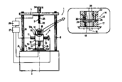
Figure 1 shows a schematic front view of a device
in accordance with the present invention;
CA 02297152 2000-O1-21
WO 99/05472 PCT/EP9$/04531
- 4 -
Figure 2 shows a schematic view of part of the
Figure 1 device;
Figure 3 shows the result of a deformation
measurement made using the Figure 1 device.
BEST MODE FOR CARRYING OUT THE INVENTION
Number 1 in Figure 1 indicates a device for
mechanically testing small-size disk-shaped specimens,
and more specifically a punch test device.
Device 1 comprises a supporting structure 2; a
mechanical pressing member 3; and an optical deformation
l0 detecting device 4.
Supporting structure 2 comprises a substantially
parallelepiped base 5; two parallel uprights 6 extending
perpendicularly from a wall 5a of base 5; and a straight
crosspiece 7 supported on uprights 6 and facing wall 5a.
Optical device 4 is fitted to wall 5a, and
comprises a support casing 8 located centrally between
uprights 6 and housing an interferometer 9 (described
later on with reference to Figure 2). Casing 8 comprises
a substantially cube-shaped central portion 10; and four
2o appendixes 11, 12, 13, 14 extending from two pairs of
opposite walls and in four directions perpendicular in
pairs and in the same vertical plane.
Central portion 10 is supported on vertical rod-
like elements 15 extending between a flat supporting
element 16 fitted to wall 5a, and a bottom wall l0a of
CA 02297152 2000-O1-21
WO 99/05472 PCT/EP98/04531
- 5 -
central portion 10 facing wall 5a, so that optical
device 4 is raised with respect to base 5.
Appendix 19 extends from a top wall 10b, opposite
wall 10a, towards crosspiece 7, and houses a mechanical
test specimen 16; while appendixes 11, 12, 13 house
component parts of interferometer 9.
More specifically, appendix 14 is tubular, and
comprises a first tubular portion 17 extending
perpendicularly to wall lOb and defining internally a
first cylindrical cavity 18 coaxial with an axis 19 and
communicating with the inside of casing 8, and a second
cylindrical cavity 20 coaxial with axis 19 and larger in
diameter than first cavity 18. Between cavities 18 and
20, first tubular portion 17 therefore defines an
1S annular shoulder 21 on which rests the peripheral edge
of specimen 16 housed inside second cavity 20. Appendix
14 also comprises a second tubular portion 22 partially
housed inside second cavity 20, connected to first
tubular portion 17 by a threaded coupling, and defining
a through hole 23 coaxial with axis 19. More
specifically, second tubular portion 22 comprises an
annular end edge 24 for pressing specimen 16 against
shoulder 21; and, when interposed between first and
second tubular portions 17 and 22, specimen 16 is
positioned perpendicular to and centrally with respect
CA 02297152 2000-O1-21
WO 99/05472 PCT/EP98/04531
- 6 -
to axis 19, and is locked axially between
shoulder 21
and annular edge 24.
Pressing member 3 is fitted to the bottom of
crosspiece 7, and comprises a cylindrical
punch 25
fitted on the end with a ceramic ball 26 smaller in
diameter than hole 23. Punch 25 extends along axis 19,
is movable, along axis 19, to and from appendix I4
by
means of a linear (e.g. pneumatic) actuat or 54 fitted
to
crosspiece 7, and engages hole 23 in appendix 14
to
position ball 26 against the face 16a of specimen
16
facing outwards of appendix 14, and so exert
a
-- controlled concentrated load on face 16a.
Linear actuator 54 and optical device 4 are
controlled by a processor 27, which provides for
controlling all the punch test operations automatically.
More specifically, linear actuator 54 is controlled by
a
control unit 28 connected to processor 27 by a serial
or
GPIB interface.
Optical interferometer 9, described later on with
reference to Figure 2, is a Michelson type, and may
operate alternatively as a white light interferometer
(using the also so-called "coherence radar"
technique),
or for ESPI (Electronic Speckle Pattern Interferometry)
measurements, or for ESPI profilometry measurements
by
simply substituting the light source and
control
CA 02297152 2000-O1-21
WO 99/05472 PCT/EP98/04531
_ 7 _
software of processor 27. The above three techniques are
complementary, supply information relative to the shape
of the specimen during and after application of the
load, and, as is known, are characterized by different
speeds and resolutions, so that one may be used in
preference to another according to the characteristics
of the specimen and the results expected.
With reference to Figure 2, interferometer 9
comprises a first branch 9a in turn comprising a beam
source 29 (housed in appendix 11) and a beam splitter 30
(housed in central portion 10) receiving a beam F from
source 29; a second branch 9b in turn comprising a
viewing device 32 (housed in appendix 12) cooperating
with beam splitter 30 and connected at the output to
processor 27; a third branch 9c in turn comprising a
reflecting device 33 (housed in appendix 13) also
cooperating with beam divider 30 and driven by a drive
circuit 34 connected to processor 27; and a fourth
branch 9d in turn comprising specimen 16 housed in
appendix 14.
More specifically, branch 9d may be defined
optically by a mirror (not shown) in place of specimen
16 for regulating interferometer 9, or by specimen 16
itself, the bottom face 16b of which defines a
retrodiffusion surface for the light from beam divider
CA 02297152 2000-O1-21
WO 99/05472 PCT/EP98/04531
_ g _
30.
Beam source 29 comprises a light source 35, and a
collimation system 36 in turn comprising a biconvex
lens. Light source 35 conveniently comprises a low-
s coherence source (e.g. a superluminescent diode with a
coherence length of a few microns) for white light
interferometer measurements, or a high-coherence source
(e.g. a laser with a coherence length of at least a
centimeter) for ESPI or ESPI profilometry measurements.
1o For ESPI profilometry measurements, the light emitted by
source 35 must be either frequency adjustable or
comprise two superimposed components of different
frequencies. The light source is controlled by a drive
and supply circuit (not shown), which may be connected
15 to processor 27 for automatically controlling the
frequency and intensity of the light emitted.
Collimation system 36 receives the light rays
produced by source 35, and generates output beam F,
which comprises rays substantially parallel to an
20 optical axis 37.
Beam splitter 30 is of known type, and is located
along optical axis 37 to receive beam F. ~ More
specifically, beam splitter 30 comprises a
semireflecting surface 38 inclined at a 45° angle with
25 respect to optical axis 37, so as to reflect part of
CA 02297152 2000-O1-21
WO 99/05472 PCT/EP98/04531
_ g _
beam F on to specimen 16 and transmit the rest of beam F
to reflecting device 33.
Reflecting device 33 is located on the opposite
side of beam splitter 30 to beam source 29, and
comprises a flat reference mirror 39 crosswise to
optical axis 37 and fitted to a position adjusting
device 40 for moving mirror 39 along optical axis 37;
and a filter 41 for adapting the light intensity of the
beam reflected by mirror 39 to that of the beam
to reflected and diffused by specimen 16. More
specifically, position adjusting device 40 comprises a
piezoelectric actuator 42 with a resolution of about 1
nm and a dynamic range of about 50 microns, and which is
fitted to a linear actuator 43 permitting controllable
incremental steps of about 1 ~.m over a total range
longer than 1 cm.
Viewing device 32 is located on the opposite side
of beam splitter 30 to specimen 16, and comprises a
telecamera 44, more specifically a black/white CCD
(CHARGE COUPLED DEVICE) telecamera; and a focusing
device 45 connected to telecamera 44 and facing beam
splitter 30. Focusing device 45 has an optical axis 46
inclined 90° with respect to optical axis 37 and
intersecting optical axis 37 at a point 47 on surface
38, and receives and focuses the light rays from beam
CA 02297152 2000-O1-21
WO 99/05472 PCTlEP98104531
- 10 -
splitter 30 on to the sensitive element (not shown) of
telecamera 44. More specifically, focusing device 45
only focuses on to telecamera 44 the incoming rays
parallel to optical axis 46.
In the Figure 1 embodiment, focusing device 45
(shown schematically) comprises a diaphragm 48 crosswise
to optical axis 46; and a pair of biconvex lenses 49, 50
crosswise to optical axis 46 and on either side of
diaphragm 48. More specifically, lens 49 is positioned
to facing a face 30a of beam splitter 30 and at a focal
distance fl from diaphragm 48; and lens 50 is positioned
facing telecamera 44 and at a focal distance f2 from
diaphragm 48. Telecamera 44 also comprises a supply
circuit 51, and is connected to processor 27 over a data
line 52 .
Device 1 operates as follows.
Before starting the test, interferometer 9 is set
by inserting a mirror (not shown) in place of specimen
16, and, in known manner, aligning and correctly
2o positioning the various optical components described
above.
Once interferometer 9 has been set, specimen 16 is
placed inside appendix 14, and, depending on the type of
measurement involved (white light interferometry, ESPI
or ESPI profilometry), the relative program is selected
CA 02297152 2000-O1-21
WO 99/05472 PCT/EP98/04531
- 11 -
on processor 27, and optical device 4 is fitted with the
necessary light source.
When the program is started, processor 27 supplies
a signal to linear actuator 54 to move punch 25 down
towards appendix 14, and, at the same time,
interferometer 9 is activated. Ceramic ball 26 is
therefore inserted inside hole 23 and positioned on to a
central portion of face 16a of specimen 16, on which it
exerts a controlled load to flex specimen I6 inwards of
io casing 8 and towards beam splitter 30. More
specifically, and as shown schematically in Figure 2,
specimen 16 (shown by the continuous line in the
undeformed position) is so stressed that a central
portion is deformed axially (as shown by the dotted
line) with respect to the peripheral portion, and
defines a bulge extending towards beam splitter 30.
Interference images related instant by instant to
the configuration of specimen 16 are generated on the
sensitive element of telecamera 44 in known manner for
2o each of the three measuring techniques mentioned above .
Briefly, the interference images are formed as follows.
Beam F produced by light source 35 impinges on beam
splitter 30; and a first fraction Fl of beam F travels
through surface 38, and impinges on reference mirror 39
by which first fraction F1 is reflected back to beam
CA 02297152 2000-O1-21
WO 99/05472 PCT/EP98/04531
- 12 -
splitter 30. The phase of the reflected portion depends
on the axial position assumed instant by instant by
mirror 39, WhlCh 1.S moved i n knnvtn mannar her
piezoelectric actuator 42 or linear actuator 43 in steps
of predetermined length and within a predetermined range
according to the type of measurement involved. More
specifically, the possibility of moving mirror 39 in
submicrometric steps enables performance of the known
"phase shifting" technique, which, by virtue of a known
l0 "phase unwrapping" algorithm in the processing software,
provides for obtaining more three-dimensional
information about the deformed specimen. First fraction
F1 is then reflected by surface 30a towards focusing
device 45 by which it is focused on to telecamera 44. A
second fraction F2 of beam F is reflected by surface 38
on to specimen 16, is retrodiffused by face 16b, and is
sent, together with first fraction F1, to telecamera 44
where first and second fractions F1 and F2 are acquired
in the form of interference images. Depending on the
2o type of software for the test being performed, the
interference images are processed to obtain three-
dimensional images of the type shown in Figure 3, which
clearly shows, both qualitatively and quantitatively,
the amount of deformation incurred. The same data,
processed differently, provides for obtaining different
CA 02297152 2000-O1-21
WO 99/05472 PCT/EP98/04531
- 13 -
spatial representations of the specimen, from which to
obtain various types of information, such as offset of
the load with respect to the center of face 16b, due,
for example, to .specimen 16 not being centered
accurately with respect to axis 19.
The resolutions obtainable with the above type of
measurement are about l0 nm (over a 3-5 ~.tm range) for
ESPI measurements, and 1 Etm (over a range of tens of
millimeters) for white light interferometry
measurements. In the case of ESPI profilometry
measurements, resolution and dynamic range depend on the
pair of frequencies selected for the light emitted by
source 35.
The advantages of the device and method according
to the present invention are as follows.
As compared with known techniques, the measuring
method described provides for obtaining better
quantitative results, especially in terms of precision
and resolution, and is more reliable.
Unlike conventional measuring techniques, the
method described supplies information relative to the
whole surface, as opposed to only the center, of the
specimen, and relative to the overall deformation
process, as opposed to only the end result. Moreover,
detailed information is also obtained relative to the
*rB
CA 02297152 2000-O1-21
WO 99/05472 PCT/EP98/04531
- 14 -
curvature and profile of the surface, and, by means of
straightforward calculations, the stress within the
structure of the material may be determined.
The method described also provides for determining
any defects or nonuniformity, and for rapidly
identifying any break regions in the specimen during
testing.
The choice of three different types of measurement,
each supplying different information according to the
type of test specimen, provides for more versatile, more
accurate measurement; and the switch from one type of
measurement to another is made extremely easily and
quickly.
Finally, as stated, the method described is fully
automatic, and supplies the operator directly at the
output with data relative to the deformed specimen.
Clearly, changes may be made to the method and
optical measuring device as described and illustrated
herein without, however, departing from the scope of the
present invention.
In particular, light source 35 may be located
outside casing 8, in which case, the light emitted is
directed into casing 8 by an optical fiber.
Also, an integrated test and measuring device may
be formed, wherein the optical and mechanical actuating
CA 02297152 2000-O1-21
WO 99/05472 PCT/EP98/04531
- 15 -
parts are housed in one structure also housing the
specimen.