Note: Descriptions are shown in the official language in which they were submitted.
CA 02297288 2009-03-10
EE ~GATE
V0jR Ci::RT3t iCAT
WO 99/07107 PCTIUS98/16369
ME7TiOD AND APPARATUS FOR INSBR7IIV(i/EX'iRAC'TING SEfS OF SIGNALS INTOfFROM A
SIGNAL S'RtBAM
RESERVATION OF COPYRIGHT
A portion of the disclosure of this patent document contains material to which
a claim of copyright protection is made. The copyright owner has no objection
to the
facsimile reproduction by anyone of the patent document or the patent
disclosure as it
appears in the Patent and Trademark Office patent file or records, but
reserves all other
rights whatsoever.
BACKGROUND OF THE INVENTION
To date, several telecommunication systems have been proposed for carrying
signals for different types of communication applications in the same signal
stream.
Some of these systems integrate signals for narrowband applications (e.g.,
telephony
signals) with signals for broadband applications (e.g., video and data
signals) in the
signal streams that they transmit. For systems that transmit integrated signal
streams
in a cell based format, the signal stream can contain a mixture of cells
having
asynchronous application signals (i.e., signals for asynchronous communication
applications) and cells having isochronous application signals (i.e., signals
for
isochronous applications).
integrated telecommunication systems, that carry different types of signals
for
different types of applications, have to properly multiplex and demultiplex
the
different signals in the signal stream. For instance, some integmted
broadband/narrowband systems have to separate the isochronous application
signals
(e.g., such as telephony signals) from the asynchronous application signals
(e.g., video
and data signals). A simple prior art method for extraating isochronous
telephony
CA 02297288 2009-03-10 II
~~~ ~ I~~"
ra,P'9k~_avATC
(~ ~f~~'i ~=s, ,.. ; ;i~~~$
~T
posaNI. ~ ~'\ 6 sC 94+1` r
WO 99/07107 2 PCT/US98/16369
signals reads alt of the bytes in a received frame into a memory and
subsequently
determines the isochronous bytes.
Figures 1 and 2 set forth one implententation of this prior art technique. As
shown in Figure 1, the prior art includes a memory 105 which sequentially
stores
every byte of a received frame in contiguous byte-wide memory locations. This
prior
art implementation also includes a table of pointers 110 with a pointer for
each
memory location. Each pointer for a memory location that stores telephony
bytes
points to a specific twisted pair 210 of a specific telephone-interface-unit
(TIU) card
205, as set forth in Figure 2. Hence, once the memory completely stores all
bytes of a
received frame, the isochronous telephony bytes in the memory are routed to
the
appropriate telephone lines by traversing the table of pointers.
This prior art technique is inefficient and memory-intensive. For instance, a
155 Mb/s SDH-like data stream having ATM and TDM cells could have 2,340 DSO
bytes. Storing this many data bytes in the memory to extract a relatively few
TDM
bytes is highly inefficient and memory-intensive.
Consequently, there is a need in the art for method and apparatus that
efficiently demultiplex signals for differwtt applications from a signal
stream. There is
also a need for method and apparatus that efficiently multiplex signals for
different
applications into a signal stream. More generally, there is a need for method
and
apparatus that identify signals for a set of communication devices in a signal
streatn
which has signals for a number of different sets of communication devices.
S~~IM 8 C(`.''~RRC~.~N CA 02297288 2009-03-10
COE A1XFICLE 3
WO 99/07107 3 PCT/US98/16369
SUMMARY OF THE INVENTION
The invention provides method and apparatus for identifying signals for a set
of communication devices in a signal stream having signals for a number of
different
sets of communication devices. Some embodiments of the invention are methods
and
devices for extracting signals for a first set of communication devices from a
signal
stream having signals for a number of different sets of communication devices.
Other
embodiments of the invention are methods and devices for inserting into a
signal
stream signals from a first set of communication devices.
Yet other embodiments of the invention are time division multiplexing and
demultiplexing methods and apparatuses that use a content addressable memory
to
identify sets of signals for a particular set of communication devices. In
addition,
some embodiment of the invention are used in fiber optic telecommunication
networks. These embodiments include an optical network unit that receives an
integrated signal stream having signals for different types of applications.
The optical
network unit includes a content addressable memory that stores locations in
the
received signal stream of signals for a first type of communication
application.
CA 02297288 2009-03-10
II
WO 99/07107 4 PCTNS98116369
BRIEF DESCRIPTION OF THE DRAWINGS
The novel features of the invention are set forth in the appended claims.
However, for purpose of explanation, several embodiments of the invention are
explained by reference to the following figures.
Figure 1 presents a memory device and a table of pointers used in one prior
art
time division demultiplexing technique.
Figure 2 presents four TIU cards used in conjunction with the memory device
and table of pointers of Figure 1.
Figure 3 presents a fiber-to-the-curb network in which the invention can be
implemented.
Figure 4 presents one example of a SDH-like frame used in some
embodiments of the invention.
Figure 5 presents one example of a telephony cell used in some embodiments
of the invention.
Figure 6 presents a common control unit for use in the network of Figure 3.
Figure 7 presents one embodiment of the invention.
Figure 8 presents one example of a content addressable memory used in some
embodiments of the invention.
i CA 02297288 2009-03-10
II
WO 99/07107 $ PCTNS98/16369
Figure 9 presents one example of a memory interface unit used in some
embodiments of the invention.
Figure 10 illustrates one manner for forwarding extracted telephony data and
control bytes to four TIUs in the network of Figure 3.
Figure 11 presents another embodiment of the invention.
*rB
CA 02297288 2009-03-10
PC'T/US98/16369
6
DETAILED DESCRIPTION OF THE INVENTION
The invention provides method and apparatus for identifying signals for a set
of communication devices in a signal streatn which has sigitals for'a number
of
different sets of communication devices. In a communication system, a
communication device is a device that transmits and/or receives signals
through the
communication system. Examples of such communication devices include computers
(such as network computers, personal computers, workstations, servers, etc.),
television set-top boxes, premises interface device, and telephones.
One or more communication devices form each set of communication devices.
A set of communication devices can include similar communication devices
(e.g., a
set of telephony conununication devices can use similar telephony equipment).
A set
of communication devices can be defined by a number of communication devices
that
utilize a similar communication medium (e.g., utilize twisted pairs or co-
axial cables)
to connect to the conununication system. In addition, a set of communication
devices
can be defined by a number of communication devices that utilize similar
communication-medium terminating devices (e.g., utilize similar line cards,
adapter
cards, modems, etc.).
In the following description, numerous details are set forth for purpose of
explanation. However, one of ordinary skill in the art would realize that the
invention
may be practiced without the use of these specific details. In other
instances, well-
known structures and devices are shown in block diagram form in order not to
obscure
the description of the invention with unnecessary detail.
CA 02297288 2009-03-10
WO 99/07107 PCT/US98/16369
7
Several embodiments of the invention are implemented in fiber-to-the-curb
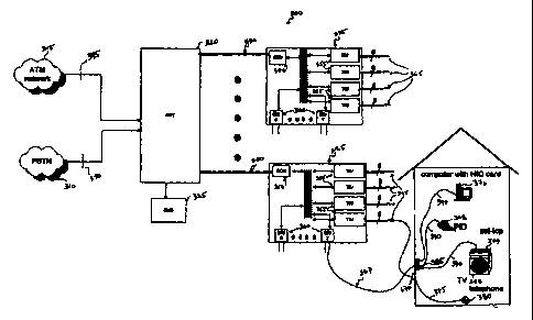
(FTTC) networks. One example of such a network is presented in Figure 3. As
set
forth in this figure, the FTTC network 300 connects one or more communication
devices at one or more network subscriber site 305 to one or more
communication
networks, such as a public switched telecommunications network (PSTN) 310, an
asynchronous transfer mode (ATM) network 315, or other communication networks.
Each network subscriber site 305 can be residential or commercial subscriber
sites.
The FTTC network 300 transmits signal streams between the subscriber sites
and the PSTN 310, the ATM network 315, or other networks (e.g., individual,
private,
or non-switched public networks). The signal streams contain signals
transmitted to,
or received from, a number of sets of communication devices. For one
embodiment of
the invention, the FTTC network transmits signals to and from telephony
communication devices (i.e., telephony application signals) and signals to and
from
non-telephony communication devices (i.e., non-telephony application signals).
For
alternative embodiments of the invention, signals for different types of
communication
devices can be transmitted through the communications network.
The FTTC network 300 includes a host digital terminal (HDT) 320, element
management system (EMS) 325, a number of fiber optic cables 330, and a number
of
optical network units (ONUs) 335. As shown in Figure 3, the HDT couples to the
PSTN, the ATM network, and/or other networks. For one embodiment of the
invention, the PSTN-HDT interface 340 follows the specification adopted by one
of
the standards bodies, such as the Bellcore specification TR-TSY-000008, TR-NWT-
CA 02297288 2009-03-10
WO 99l07107 PCT/US98/16369
_ 8 -
000057 or TR-NWT-000303. The physical interface to the PSTN can be twisted
pairs
carrying DS1 signals, or fiber optic cables carrying OC-3 optical signals.
The ATM network-HDT interface 345 can be realized using an optical
interface (such as OC-3, OC-12c, etc.). For one embodiment of the invention,
the
HDT 320 has two optical broadcast ports, which can only receive signals
carrying
ATM cells, and one optical interactive port which can receive and transmit
signals.
The HDT receives downstream signals from the PSTN, the ATM network, or
other networks, and routes these signals downstream to the network subscriber
sites. It
also receives upstream signals from the network subscriber sites, and routes
these
signals upstream to the PSTN, the ATM network, or other networks.
On the downstream side of the network, the HDT serves a multiplexor which
(1) controls access of the received downstream signals (i.e., the signals it
receives from
the PSTN, ATM, or other networks) to the transmission media, and (2) transmits
the
received signals to the appropriate ONUs 335 via the appropriate fiber optic
cables
330. Conversely, on the upstream side of the network, the HDT serves as a
demultiplexor which (1) parses the received upstream signals (i.e., the
signals received
from the ONUs) into signal streams for the PSTN, ATM, or other networks, and
(2)
supplies these signal streams to the appropriate network.
The HDT also re-formats the downstream and upstream signals, before
forwarding them to their destinations. As further described below, the HDT
performs
the following formatting operations: combining isochronous and asynchronous
signals
into frames, parsing integrated frames into individual signal streams,
adjusting signal
CA 02297288 2009-03-10
WO 99/07107 PCT/US98/16369
9
rates, and converting of electrical signals to and from optical signals. One
of ordinary
skill in the art would realize that, in alternative embodiments of the
invention, the
HDT does not perform all of these formatting operations, or performs
additional
operations.
In the FTTC network set forth in Figure 3, the HDT combines (i.e., maps) the
received downstream signals into frames containing a mixture of cells having
asynchronous application signals (such as data and video signals) and cells
having
isochronous application signals (such as telephony signals). The HDT transmits
these
frames to the ONUs at a prespecified rate (e.g., once every 125 s). The HDT
also
parses the received upstream frames into individual bytes supplied to the
PSTN, ATM,
or other networks.
Figure 4 presents one example of frames transmitted across the fiber optic
cables 330. Each frame shown in this figure is a SDH-like frame which includes
overhead and payload envelopes. The payload envelope includes 41 cells of
asynchronous and isochronous information. Each cell has 57 bytes.
Figure 5 presents one example of an isochronous, telephony cell. As shown in
this figure, each cell includes three reserved bytes (R), and six groups of
DSO bytes.
Figure 5 presents each group as eight DSO data bytes following one signaling
byte (S).
The signaling byte contains the status and control signals (e.g., on/off hook,
ring, etc.)
for the eight DSO bytes. Alternatively, each group can include nine clear DSOs
bytes
containing a mix of information and control signals.
CA 02297288 2009-03-10
WO 99/07107 PCT/US98/16369
The HDT also adjusts the signal rate of the data it receives. For instance,
for
some embodiments of the invention, the HDT 320 converts the signals it
receives from
the PSTN 310 at a DS 1-rate to signals at a DSO-rate; it then transmits these
signals to
the ONUs in the SDH-like frames. On the upstream side, the HDT performs the
5 inverse signal rate transformation operation. The HDT also converts the
electrical
representation of the digital signals into an optical representation, and visa
versa.
As shown in Figure 3, the HDT couples to the EMS 325. The EMS is used to
provision services and equipment on the FTTC network (e.g., allocate twisted
pairs off
the TIUs), in the central office where the HDT 320 is located, in the field,
or in the
10 residences. The EMS is software based and can run on a personal computer in
which
case it will support one HDT and the associated access network equipment
connected
to it. Alternatively, it can run on a workstation in which case it will
support multiple
HDTs and access networks,
The fiber optic cables 330 communicatively couple the HDT to a number of
ONUs 335 located in a number of serviced areas. Some embodiments of the
invention
use bi-directional, single-mode fiber lines and a dual wavelength transmission
scheme
to communicate between the ONUs and the HDT. In addition, some embodiments of
the invention use sixty four optical fiber cables to connect the HDT to sixty
four
ONUs.
As shown in Figure 3, each ONU includes a common control unit (CCU) 350,
four telephone interface units (TIU) 355, and eight broadband interface units
(BIU)
CA 02297288 2009-03-10
WO 99/07107 PC.T/1J598/16369
. 11
360. The CCU controls the operation of the ONU. In particular, the CCU
performs
similar formatting operations as those performed by the HDT.
For instance, the CCU (1) parses the received downstream signals (i.e., the
frames it receives from the HDT) into telephony application signal streams and
non-
telephony application signal streams, and (2) supplies the telephony
application signal
streams to the appropriate TIU 355. The CCU aiso combines the signal streams
that it
receives from the TIUs 355 and BIUs 360 into SDH-like frames (such as the
frames
discussed above with respect to Figure 4), which it then transmits to the HDT
via fiber
optic cable 330. Different embodiments of the invention can be employed in the
CCU,
in order to allow the CCU to perform the above-described parsing (i.e.,
demultiplexing) and combining (i.e., multiplexing) operations. Two such
embodiments will be described below by reference to Figures 7 and 11.
Figure 6 presents one example of the CCU 350. As shown in this figure, the
CCU includes a bi-directional (BIDI) optical converter 605, a framer 610, a
TIU
interface (TIUI) 615, a BIU interface (BIUI) 620, and a microprocessor 625. On
the
downstream side, the optical converter 605 converts optical signals, that it
receives via
a fiber optic cable 330, into a serial, electrical signal stream. The framer
610 then
receives this bit-wide electrical sigoal stream and oonverts it into a byte-
wide signal
stream. On the upstream side, the optical converter receives bit-wide,
electrical signals
from the fratner, and converts these electrical signals into optical signals
for
transmission via the fiber optic cable 330.
CA 02297288 2009-03-10
WO 99/07107 PGT/US98/16369
_ 12
The framer also scans the incoming signal stream in order to determine the
frame boundary information used to determine the location of payload and
overhead
bytes. Once the framer determines the frame boundary, it generates a frame
synch
signal which indicates the start of each frame. As described below, this frame
synch
signal is used by a number of the circuits of the CCU.
The framer communicatively couples to the TIUI 615, in order to transmit and
receive signals from the TIUI. Some embodiments of the invention are
implemented
in the TIUI, in order to allow the TIUI to parse the telephony application
signals from
the downstream signal stream, and to combine the telephony application signals
into
the upstream signal stream. Two such embodiments will be described below by
reference to Figures 7 and 11.
The framer also transmits signals to and receives signals from the BIUI. The
BIUI perfonns administrative functions (e.g., parity check and overhead
addition
functions). On the downsb-eam side, the BIUI forwards the signals it receives
from the
framer to the B1Us 360. Each individual BIU then extracts the portion of the
received
signals that are addressed to it; the BIU forwards the extracted signals to a
network
subscriber site 305. On the upstream side, the BIUI 620 acts as an arbitrator
for the
BIUs. In this capacity, the BIUI allocates different portions of each frame's
payload to
different BIU's.
The microprocessor 625 of the CCU 350 is used to program various
components of the CCU. For instance, as further described below, the
microprocessor
is used to program various components of the TIUI. Through this programming,
the
CA 02297288 2009-03-10
WO 99/07107 PCT/US98/16369
- 13 -
TIUI can store the location of telephony bytes in the received or transmitted
signal
stream.
As shown in Figure 3, each ONU 335 includes four TIUs 355 coupled to the
TIUI 615 through a backplane interconnect. Each TIU 355 connects to six
twisted
pairs 365, which thereby allow each ONU to service up to twenty four network
subscriber sites. For altemative embodiments of the invention, the FTTC
network 300
utilizes ONUs that have different number of TIUs and/or different number of
twisted
pairs for each TIU.
When a TIU receives a signal stream from the CCU, it converts the signal
stream into a signal stream for a narrowband service (such as plain old
telephony
signals (POTS), coin, ISDN, etc.). For instance, the TIU can generate analog
POTS
which it transmits to network subscriber site 305 via a twisted pair 365. At
the
network subscriber site 305, a network interface device (NID) 370 serves as an
interface and demarcation point between the twisted pair 365 and subscriber-
site
twisted pair 375 coupled to telephone 380. The NID provides high-voltage
protection.
In addition, through the NID 370 and twisted pairs 365 and 375, each TIU 355
receives analog signals from the network subscriber site. It then converts
these analog
signals into digital signals which it supplies to the CCU.
Each ONU 335 also includes eight BIUs 360 coupled to the CCU 350 through
the backplane interconnect. Each BIU 360 eonnects to two co-axial cables.
Altemative number of BIUs and/or co-axial cables could also be used in the
ONU. As
CA 02297288 2009-03-10
wo 99ro7107 14 PCT/US98/16369
described above, each BIU communicativety couples to the BIUI 620 of the CCU
350.
Through this coupling, the BIU receives signals from the CCU.
The BIU inciudes a filter which decodes a portion of the overhead bytes of
each received cell to determine if the received cell is addressed to its BIU.
If so, the
filter also detennines the addressed co-axial cable of the BIU. The filter
then
reformats the received cell and stores it in a FIFO queue. As the contents of
the FIFO
are read out, the BIiJ modulates the read-out signais onto an RF carrier and
transmits
the data via the addressed co-axial cable to a splitter 385 at the network
subscriber site
305.
Subscriber-site coaxial cables 390 couple the splitter to a number of
communication devices at the network subscriber site. These communication
devices
include a television (TV) 392 with a television set-top 394, computer with a
network
interface card (NIC) 396, and a premises interface device (PID) 398 connected
to a
telephone. Each of these devices parses and decodes the received reformatted
cells in
order to obtain video, data, and voice signals.
In particular, each communication device requires an interface sub-system
which provides for the conversion of the signal from the forniat on the
subscriber-site
coaxial cable to the service interface required by the device. The PID 398
extracts the
voice signals carried on the subscriber-site coaxial cable 390 and generates a
telephone
signal compatible with the telephone. Similarly, the television set-top 394
converts
digital vidoo signals to analog signals compatible with the TV 392. The NIC
card
generates a computer compatible signal.
CA 02297288 2009-03-10
WO 99/07107 PCT/US98/16369
Through the subscriber-site coaxial cables 390, the splitter 385, and the
coaxial
cable 367, the BIU also receives broadband signals for upstream transmission
through
the FTTC network 300. The BIU demodulates the signals that it receives and
combines the resulting components of the broadband signals into a unified
broadband
signal stream, which it relays to the BIUI 620.
One of ordinary skill in the art would understand that the invention can be
implemented in other FTTC networks, For instance, some embodiments of the
invention can be implemented in the networks disclosed in United States Patent
No. 6,282,189, entitled "Unified Access Platform for Simultaneously Delivering
Voice and Cell-based Services". Alternatively, one of ordinary skill in the
art would
understand that the invention can be implemented in alternative networks.
One embodiment of the invention that is implemented in the FTTC network
300 extracts signals for a set of telephony comrnunication devices from an
integrated
telephony/non-telephony signal stream transmitted through the FTTC network.
This
embodiment stores position identifying indicia (e.g., pointers) that identify
the
locations of telephony application signals in a received signal stream, which
as
mentioned above, is organized in a SDH-like fraune.
It then generates position identifying indicia as it receives a transmitted
frame,
and simultaneously compares this indicia to more than one of the stored
indicia. When
CA 02297288 2009-03-10
WO 99/07107 PCT/US98/16369
- - 16
the generated indicia matches a stored indicia, the process extracts the
telephony signal
corresponding to the generated indicia from the received signal stream. This
process
then generates appropriate routing signals based on the matched stored
location, in
order to route the extracted set of signals to its set of communication
devices.
Figure 7 sets forth one such embodiment. This apparatus is implemented in
the CCU's TIUI 615, and serves as the interface to the TIUs of the ONU 335.
This
interface constantly receives the SDH-like frames in byte-wide increments at
the SDH-
like 19.44 MHz. The interface includes a byte counter 705, a content
addressable
memory 710, a memory interface unit 715, swing data random access memories
720, a
control random access memory (RAM) 725, a downstream TIU interface 730, a
table
of pointers 735, a pointer RAM control 740, a bit counter (not shown), a
microprocessor interface unit 745, and a downstream synchronizing unit (not
shown).
The counter 705 and content addressable memory (CAM) 710 in conjunction
act to identify the telephony application signals in the downstream SDH-like
frames
forwarded to the memory interface unit 715. Specifically, the counter receives
frame
synchronizing signal (generated by the framer 610) to maintain its alignment
to each
frame. The counter also receives a synchronizing signal from the downstream
synchronizer (not shown). This synchronizing signal maintains the counters in
the
SDH-domain and the counters in the telephony-doniain in synch, so that the
interface
units 715 and 730 in these domains do not simultaneously access the memories
720
and 725.
The counter also receives the 19.44 MHz SDH-byte clock to generate three
count values that are synchronous with the signals received in byte-wide sets
at this
CA 02297288 2009-03-10
WO 99/07107 PCT/US98/16369
- 17
frequency. In other words, the counter is a byte counter which generates sets
of count
values. Each set of count values serves as a pointer that specifies the
location of a byte
within a frame received by the memory interface unit 715. Each pointer is
input to the
CAM to determine if the received byte corresponding to the pointer is a
telephony
application byte.
As mentioned above by reference to Fignres 4 and 5, some embodiments of
the invention are designed to multiplex and demultiplex SDH-like frames with a
payload of 41 cells of telephony application signals (e.g., TDM signals) and
aon-
telephony applications signals (e.g., ATM signals). Each telephony cell is
composed
of 6 groups of 9 bytes. The 9 bytes are arranged as one signaling byte
followed by 8
DSO bytes.
Given this cell structure, the counter genen3tes (1) a cell count value,
RxCellCnt, that specifies the cell count of the currently received byte, (2) a
group
count value, RxGrpCnt, that specifies the group count of the currently
received byte,
and (3) a DSO byte count, RxDSOCnt, that specifies the byte count of the
currently
received byte. In this manner, the three count values serve as pointers that
uniquely
identify every byte within each of the 41 potential TDM cells.
The behavior of these three counts is shown below.
CellCnt: n-1 ~ ------------------------------ n -----------------------
--
GroupCnt: 5 ~ 7(------- 0------- I ------- 1------- I ------- 2------
-1
DSOCount:
4l5l6l7l0l1l8l0l112l31415161718101112131415161718101112131415161
71
C 11Cnt: ------------------------------- n ---------------------- { --- n+1
CA 02297288 2009-03-10 ii
WO 99/07107 PCT/US98/16369
18 .
GrpCnt: 171 ------- 3------- ~------- 4------- ~------- S------- 1 7 1--
0-
DSOCount:
12181011121314151617181011121314151617181011121314151617101118lOI
l~
The DSO number 8 within each group is used as the super-frame, multiplexed
signaling byte. Also, within each cell there are three reserved bytes
corresponding to
group 7 with a DSO count of 0,1 or 2.
As shown in Figure 7, the CAM 710 receives the generated count values
(RxCelICnt, RxGrpCnt, and RxDSOCnt) and receives a signal (RxCeIlType)
indicating
the type of the received cell. A CAM is a memory device with the ability to
compare
any set of signals (e.g., a data word) presented to it with all of the CAM
contents at
once, and report the location in the CAM whose contents match the presented
set of
signals. In the prior art, CAMs have been used in bridges and routers to
compare
extracted MAC addresses with stored MAC addresses, in order to detennine if
received packets are addressed to LANs connected to the bridges or routers.
Figure 8 presents one example of the CAM 710 that can be used in some
embodiments of the invention. As shown in this figure, the CAM includes
control
circuitry 805, a first memory 810, a second memory 815, downstream comparators
820, and decoder 825. Although this figttte presents two memories, one of
ordinary
skitl in the art would appreciate that this presentation is simply a pictorial
representation of the CAM in order to facilitate its description, and that
these two
memories could be part of a single memory array.
i CA 02297288 2009-03-10 ii
wo 99/07107 PCT/US98/16369
19 -
Through microprocessor interface unit 745 and the control circuitry 805, the
first and second memories couple to the microprocessor, 625 to receive
respectively
data signals (i.e., position identifying indicia) and control signals (e.g.,
block size
indicia) for storing. Specifically, through this coupling, the first memory
810 receives
and stores up to thirty two position identifying indicia that identify the
position of
thirty two telephony-application bytes in each SDH-like &ame.
In some embodiments of the invention, the first memory stores thirty position
identifying indicia, where each position identifying indicia is a pointer that
specifies
the location of a telephony-application byte within each frame received by
memory
interface unit. When the frames have a structure as shown in Figure 4, and the
telephony cells have structures as shown in Figure 5, each stored pointer can
have
thirteen bits. Of these bits, six bits identify the cell value, three bits
identify the group
value, and four bits identify the byte value.
In the second memory 815, the microprocessor stores control bits that
determine the size of the blocks of signals extracted from the signal stream.
In some
embodiments of the invention, the second memory stores thirty two sets of
control
bits, so that there is one set of control bits for each pointer in the first
memory. Each
set of control bits includes two bits. When a received byte has its location
in the
received itame match one of the stored pointers in the first memory, the
memory
interface unit decodes the two control bits corresponding to the matched
pointer in
order to determine whether it needs to extract one to three bytes following
the received
byte in the received signal stream in addition to extracting the received
byte.
CA 02297288 2009-03-10
WO 99107109 PCT/US98/16369
As mentioned above, the CAM also includes thirty-two comparators 820. Each
comparator compares a paracular thirteen-bit pointer stored in the first
memory with
the thirteen-bit output of the byte counter 705. For instance, the comparator
for the nth
row in the first memory array receives the bits stored in row n (Rn) from
columns 0 to
5 12 (CO and C 12), and compares these bits to the generated thirteen count
bits
RxCelICnt, RxGrpCnt, and RxDSOCnt.
Each comparator includes thirteen X-NOR gates, with each X-NOR gate
receiving one bit of the stored pointer and one bit of the generated count
value. Each
comparator also has an AND gate (not shown) which receives the outputs of the
10 thirteen X-NOR gates of the comparator. The output of each AND gate then
represents the output of the comparator. Hence, the thirty two comparators 820
have
thirty two output lines. When a received byte's location matches a stored
pointer, the
pointer's comparator indicates a hit (i.e., a match) by pulling its output
line high. One
of ordinary skill in the art would understand that altenlative CAM structures
are used
15 in alternative embodiments of the invention.
As further described below, the memory interface unit 715 reeeives the thirty
two bit output of the comparators 820. This interface unit includes a priority
encoder
which receives this thirty two bit output to generate a five bit output to
represent the
address of the row storing the matched pointer in the first memory. The row
address
20 for the matched pointer is the same as the row address for its
corresponding pair of
control signals in the second memory. Hence, the five bit address is supplied
to the
decoder 825 of the second memory. This decoder then latches and outputs the
two
control bits stored at the row identified by the received address signal. The
memory
CA 02297288 2009-03-10
WO 99/07107 PCT/U398/16369
- 21
interface unit then receives these two bits, which, as described tater, direct
the interface
unit to extract up to three bytes that follow the received byte.
The CAM also receives the CeIlType signal (such as RxCeIlType or
TxCellType). This signal indicates whether the cell that is currently being
received in
the received frame is a telephony cell or a non-telephony cell. To generate
this signal,
the CCU includes a memory (not shown) with forty one registers for the forty
one cells
in the frame payload. Each register stores a CeilType flag that indicates
whether its
corresponding cell is a telephony cell. By using the cell count address
generated by
the counter 705, the CCU sequentially reads the forty one registers to
generate the
Ce1lType signal. When the cell is not a telephony cell, the value of the
CeIlType
signal powers down the comparators 820.
As mentioned above, the memory interface unit 7] 5 of Figure 7. This
interface unit receives the downstream signal stream. It also receives the
generated
count values RxGrtpCnt and RxDSOCnt, and the RxCellType, in order to
syncbronously operate with the CAM. It couples to the CAM 710 to receive its
thirty-
two bit output. Based on this output, it generates the five bit address of the
matched
pointer in the CAM. The interface unit then uses this address to retrieve the
two
control bits corresponding to the matched pointer from the CAM. Based on the
two
control bits, as well as the thirty two output bits of the CAM, the interface
unit extracts
one to four telephony bytes from the received signal stream, and generates
address and
control signals to store the extracted telephony bytes in data and control
RAMs 725
and 730.
CA 02297288 2009-03-10
W0 99/07107 PCTlUS98/16369
22
Figure 9 presents one example of the memory interface unit 715. This
embodiment includes a priority encoder 905, an OR gate 910, and a downstream
(DS)
state machine 915. Priority encoder 905 receives the thirty two bit output of
the CAM.
As the CAM does not store identical pointers, only one of the thirty two
output lines
should be active when a telephony signal is received. If the CAM reports
multiple hits
on its thirty two output lines (i.e., if more than one line is active), it is
determined that
the CAM was improperly progranimed, and an error condition is reported through
an
intenupt structire or a status flag.
When one of the thirty two output lines 755 are active, the priority encoder
generates a five bit address based on the values of the active line. This
address is sent
back to the CAM in order to mtrieve two control bits which are stored in the
second
memory at the generated row address. These two bit are then supplied to the DS
state
machine.
The state machine also receives an enable signal 920, as well as the five-bit
output of the encoder. The enable signal is the output of the OR gate 910,
which
receives as its input the thirty two output lines of the CAM. When one of
these lines is
active, the OR gate output is also active. This active signal causes the DS
state
machine to extract from the downstream signal stream the byte that it is
receiving at
that time. By decoding the two control bits, the DS state machine then
determines
whether it needs to extract up to three other bytes that follow the initial,
extracted byte.
Based on the value of the generated five bit address and the two control bits,
the state machine 915 generates address and control signals to store the
extracted bytes
CA 02297288 2009-03-10
WO 99107107 PCT/US98/16369
23 -
in the data and control RAMs 720 and 725. For some embodiments of the
invention,
the relationship between the pointers stored in the CAM and the storage
locations in
RAMs 720 and 725 (for storing exttacted bytes whose locations in the signal
stream
matched the stored pointers) is hard coded. This bard coded relationship
allows the
downstream state machine to simply use the five bit row address 925 of the
matched
pointers to generate the address signals for the locations in the RAMs 720 and
725 for
storing the extracted bytes.
In some embodiments of the invention, the memory interface unit is designed
by using a hardware design language. For such embodiments, one possible design
of
the memory interface unit is set forth in Appendix A. This design uses the
Verilog
hardware design language. Numerous manufacturers of logic synthesizers (such
as
Synopsys, Viewlogic, Synplicity, ACEO, Cascade Design Automation, Exemplar,
and
Altera) can transform the logic in this code to gates, and thereby obtain the
gate level
implementation for the memory interface unit.
The memory interface unit extracts either telephony data signals or telephony
control signals from the fiwme. The two signal types are treated differently
in the way
they are stored. The control signals are written to control RAM 725, whereas
the data
signals are written to data RAM 720. In some embodiments of the invention, the
control RAM is a 128x8, dual port RAM, while the data RAM is formed by two
32x32, dual port RAMs that act as a "swing" buffer ("ping-pong" buffer).
RAMs 720 and 725 are where the telephony data and control signals cross from
the 19 MHz, SDH-like time domain into the 4 MHz, telephony domain (e.g., POTS
CA 02297288 2009-03-10
Wo 99107107 PCT/US98116369
24 -
domain). Two RAMs are used to form the "swing" buffer for the telephony data
signals. 'fhe "swing" buffer has two rnemory areas so the 19 MHz domain can
write
the data for one frame, while the 4 MHz domain can read the data for the
previous
frame. The memory interface unit 715 determines which of the "swing" RAMs to
store the telephony data signals in the current frame, based on a frame count
generated
by a frame counter (not shown).
The control signals do not require more than one RAM to cross the 19 MHz - 4
MHz boundary. This is because the frequency of the control signals is slow
enough
that both the 19 MHz and the 4 MHz domains can access the RAM before the next
signaling byte will appear in the SDH frame. Also, a slight degree of
imprecision can
be tolerated with respect to the control signals, as such imprecision will
hardly be
noticed by the users. The 4 MHz side is given priority over the 19 MHz side in
the
accessing of this control signal RAM.
Once the ONU has completely received a frame, the counter 705 and the CAM
710 have checked the location of each received byte, and the memory interface
unit
715 has extracted and stored all the telephony data and control signals of the
frame in
the data and control RAMs, the pointer RAM control 740, the table of pointers
735,
and the DS TIU interface 730 direct the telephony signals in RAMs 720 and 725
to the
appropriate TIUs. In other words, the pointer RAM control 740, the table of
pointers
735, and the DS TIU interface 730 act as a cross connect structure that
determines
which data and control is forwarded to which T.
CA 02297288 2009-03-10
WO 99l07107 PC,'lYU898/16369
As shown in Figare 7, the DS TIU interface 730 couples to four TIUs A, B, C,
and D. This interface also couples to the pointer control 740 to receive
addresses of
locations in the data and control RAMs that it needs to read. The pointer
control
retrieves these addresses from the pointer table 735. The poiater table
couples to the
5 microprocessor 625 through the pointer control 740 and the microprocessor
interface
unit 745, in order to reoeive and store address signals from the
microprocessor during a
progmm mode.
The pointer control 740 serves as an arbitor which controls access to the
table
735. The pointer control receives the 4.096 MHz clock signal, the frame synch
signal,
10 and the DS synch signal. A bit counter (not shown) of this pointer control
receives the
4 MHz clock signal to generate a nine-bit count at this frequency. The control
unit
receives the frame synch signal (generated by the &amer 610) to maintain its
alignment to each frame. The control unit 740 receives the DS synch signal
from the
downstream synchronizer (not shown), in order to synchronize its counter with
the
15 SDH-domain counters so that the interface units 715 and 730 do not
simultaneously
access the memories 720 and 725.
The top six bits of the nine-bit count produced by the pointer control's
counter
serves as a byte counter that counts sixty four bytes for each received frame.
These
sixty four count values define sixty four time slots during which the pointer
control
20 740 (1) causes the pointer table 735 to generate 256 addresses in the RAMs
720 and
725, and (2) supplies these 256 addresses to the DS TILJ interface 730.
CA 02297288 2009-03-10
WO 99/07107 PCT1US98/16369
= 26
In pardcular, during each of the sixty four time slots, the pointer RAM
control
directs the table 735 to output in a particular sequence the contents of four
of its nine-
bit wide storage locations. Each nine-bit wide storage location of the table
735
includes seven bits for defining a row address, one bit for selecting the
control RAM,
and one bit for selecting the data RAM. In turn, during each of the sixty four
time
slots, the TIU interface 730 reads the RAMs at each of the four addresses
output by the
table. The TIU intexface then forwards the four sets of retrieved signals to
the four
'I'IUs A, B, C, and D.
Figure 10 iliustrates this read out operation pictorially for one embodiment
of
the invention which stores 120 telephony data bytes in each data RAM 720, and
stores
120 telephony control bytes in the control RAM 725. During the first two time
slots
and the last two time slots, the DS TIU interface reads out overhead bytes
(e.g., parity
bytes)_
During the remaining sixty time slots, four sets of thirty telephony data
bytes
(D), and four sets of thirty telephony control bytes (C) are respectively read
out of the
data RAMs 720 and the control RAM 725. Each'ITU 355 receives one set of
telephony data bytes and one set of telephony control bytes. For the operation
illustrated in Figure 10, the pointer RAM control 740 alternatively reads out
telephony
data bytes and telephony control bytes for each TIU.
Data and control signal fetching are done for each of the TIU in a particular
order. During each of the middle sixty time slots, the DS TIU interface 730
retrieves
four telephony bytes, The first three bytes for three TIUs are stored in
intermediate
CA 02297288 2009-03-10
wo 99/07107 PCTN398f16369
27
registers. When the fourth byte is fetched, all four bytes are written to
shift registers.
These bytes are then shifted out to the TIUs one bit at a time based on the
value of the
pointer control's bit counter. While the bytes in the shift registers are
being shifted
out, the next four telephony bytes are fetched.
In some embodiments of the invention, the DS TIU interface 730 and the
pointer control 740 are designed and manufaetuced by using a hardware design
language. For such embodiments, one possible design for the DS TIU interface
unit is
set forth in Appendix B, while one possible design for the pointer contrrol
740 is set
forth in Appendix C. These designs use the Verilog hardware design language.
Numerous manufacturers of logic synthesizers (such as Synopsys, Viewlogic,
Synplicity, ACEO, Cascade Design Automation, Exemplar, and Altera) can
transform
the logic in this code to gates, and thereby obtain the gate level
implementation for the
DS TIU interface.
Another embodiment of the invention that is implemented in the FTTC
network 300 muitiplexes telephony application signals and non-telephony
application
signals to form an integrated telephony/non-telephony signal stream for
transmission
to the HDT 320 through the F1TC network. This embodiment stores position
identifying indicia (e.g., pointers) that identify the appropriate location of
the
telephony signals in a signal strearn, which as mentioned above is organized
in a SDH-
like frame. It then generates position identifying indicia as it receives
signals for
transmission, and compares the indicia to the stored indicia. When generated
indicia
matches stored indicia, it inserts the telephony signal con=esponding to the
generated
indicia in the signal sttum.
CA 02297288 2009-03-10
WO 99/07107 PCT/US98/16369
28 =
Figure 11 sets forth one such embodiment of the invention. This embodiment
multiplexes telephony signals and non-telephony signals to form an integrated
telephony/non-telephony signal stream for transmission to the HDT 320 through
the
FTTC network. The interface appara.tus 1100 constantly receives four telephony
data
streams (e.g., four DSO streams) from four TIUs A, B, C, and D. It multiplexes
these
streams with another signal stream to form a byte-wide stream supplied to the
framer.
Like the apparatus 700 of Figare 7, the apparatus 1100 of Figure 11 can be
iinplemented in the CCU's TIUI, which serves as the interface between the TIUs
and
the fiber optic cables. Also, like apparatus 700, this apparatus has a byte
counter 1105,
a CAM 1100, a memory interface unit 1.115, two dual port data RAMs 1120, a
dual
port control RAM 1125 , an upstream (US) TIU interface 1130, a table 1135, a
pointer
contro11140, and a microprocessor interface unit 1145. However, it also
includes a
delay FIFO 1150, an early counter 1155, and a set of eight OR gates 1160.
The operation of the apparatus 1100 is similar to the operation of the
apparatus
700, except that it is in the reverse order and it has a built in delay. For
instance, like
the pointer control 740, the table 735, and the DS TIU interface 730, the
pointer
control 1140, the table 1135, and the US TIU interface 1130 act as a cross
connect
structure. However, unlike these structures of apparatus 700, the pointer
control 1140,
the table 1135, and the US TIU interface 1130 forward the signals coming from
the
TIUs to the RAMs 1120 and 1125.
As shown in Figure 11, the US TIU interface 1130 couples to TIUs A, B, C,
and D to receive telephony data and control bytes. This interface also couples
to the
CA 02297288 2009-03-10 ii
wo 99/07107 PCT/US98/16369
29 _
table 1135 via the control unit 1140 to receive addresses of locations in the
data and
control RAMs 1120 and 1125, in which it can store the received telephony
bytes. The
table 1135 couples to the microprocessor 625 through the control unit 1140 and
the
microprocessor interface unit 1145, in order to receive and store address
signals from
the microprooessor during a program mode.
The table 1135 is controlled by the pointer control 1140, which includes a bit
counter (not shown). This control unit receives the 4.096 MHz clock signal,
the frame
synch signal, and the US synch signal. The contml unit's bit counter receives
the
4.096 MHz clock signal to generate a nine-bit count at this frequency. The
control unit
receives the frame synch signal (generated by the framer 610) to maintain its
alignment to each frame. The control unit 1140 receives the US synch signal
from the
downstream synchronizer (not shown), in order to synchronize its counter with
the
SDH-domain counters so that the interface units 1115 and 1130 do not
simultaneously
access the memories 1120 and 1125.
The top six bits of the nine-bit count produced by the pointer control's
counter
serves as a counter that counts sixty four time slots for each transmitted
frame. During
these sixty four time slots the pointer contro11140 (1) causes the pointer
table 1135 to
output 256 addresses in the RAMs 1120 and 1125, and (2) supplies these
addresses to
the US TIU interface 1130. The US TIU interface then uses these 256 addresses
to
store 256 bytes fi+om the TIUs 355 in the R.AM 1120 and 1125.
More partieularly, during each of the sixty four time slots, the US TIU 1130
receives and stores up to four telephony bytes from the four TIUs A, B, C, and
D.
CA 02297288 2009-03-10
wo 94ro7107 PCT1US98/16369
Also, during each time slot, the pointer RAM control 1140 directs the table
1135 to
output four of its nine-bit wide storage locations. Each nine-bit wide storage
location
in the table 1135 includes seven bits for defining a row address, one bit for
selecting
the control RAM, and one bit for selecting the data RAM. The US TIU interface
then
5 uses the nine-bit outputs of the table to store its four telephony bytes in
the RAMs
1120 and 1125.
As mentioned above, in some embodiments of the invention, the pointer RAM
control 740 is designed and manufactured by using a hardware design language;
one
example of such a design is set forth in Appendix C. Also, in some embodiments
of
10 the invention, the US TIU interface 1130 is designed and manufactured by
using a
hardware design language. For such embodiments, one possible design of the US
TIU
interface is set forth in Appendix D. This design uses the Verilog hardware
design
language. Numerous manufacturers of logic synthesizers (such as Synopsys,
Viewlogic, Synplicity, ACEO, Cascade Design Automation, Exemplar, and Altera)
15 can transform the logic in this code to gates, and thereby obtain the gate
level
implementation for the US TIU interface.
The memory interfaoe unit 1115 also accesses the data and control RAMs 1120
and 1125. However, unlike the US TTU interface 1130 which couples to the 4.096
MHz ports of these RAMs, the memory interface unit 1115 couples to the 19.44
MHz
20 ports of these RAMs. As shown in Figure 11, the memory interface unit also
couples
to the CAM 1110, the early counter 1155, the counter 1105, and the delay FIFO
1150,
in order to read the telephony bytes from the RAMs and timely output these
bytes in a
signal stream for ttansmission.
CA 02297288 2009-03-10
WO 99/07187 PCT/US98/16369
- 31
Specifically, the early counter 1155 cause memory interface unit to read out
the
telephony signals from the RAMs and to store them in the delay FIFO 1150. The
count values generated by the early counter are a predetermined number of
bytes (e.g.,
twenty four) ahead of the count values generated by the counter 1105. The
early
counter 1155 generates count values which identify the locations (or time
slots or time
periods) in the frame for transmission.
These count values are supplied to the CAM 1110. One example of this CAM
is depicted in Figure 8, which was discussed above. The CAM 1110 can store up
to
thirty two pointer in a first memory, where each pointer specifies the
location of a
telephony-appGcation byte within each frame for transmission. The CAM also
stores
two control bits for each pointer in a second memory.
Once the CAM receives a count value from the early counter, it simultaneously
compares the count value with all of its pointers. If the generated count
value matches
one of the CAM's stored pointers, the CAM outputs a hit signal on the output
line for
its matched pointer.
The memory interface unit 1115 receives the thirty two output lines of the
CAM. When the CAM outputs a hit signal, the memory interface unit (like the
memory interface unit 715 of apparatus 700) uses a priority encoder to encode
the
signal on the thirty two output lines into a five bit output. This five bit
output
represents the address of the row storing the matched pointer. This output is
feedback
to the CAM in order to read out the pair of control signals corresponding to
the
matched pointer. The memory interface unit then receives these two bits.
CA 02297288 2009-03-10
WO 99/09107
PCT/U398116369
32
For some embodiments of the invention, the relationship between the pointers
stored in the CAM 710 and the storage locations in RAMs 1120 and 1125 is hard
coded. This hard coded relationship allows the memory interface unit to use
the
matched pointer's row address plus the retrieved two control bits to extract
one to four
bytes from the RAMs 1120 and 1125. In some embodiments of the invention, the
memory interface unit 1115 is designed and manufactund by using a hardware
design
language. For such embodiments, one possible design of the memory interface
unit is
set forth in Appendix E. This design uses the Verilog hardware design
language.
Numerous manufacti aers of logic synthesizers (such as Synopsys, Viewlogic,
Synplicity, ACEO, Cascade Desiga Automation, Exemplar, and Altera) can
transform
the logic in this code to gates, and thereby obtain the gate level
implementation for the
memory interface unit 1115.
The memory interface unit stores the extracted telephony data bytes in the
delay FIFO 1150, while it stores some of the extracted telephony control bytes
in a
circulat buffer. As mentioned above, the early counter is a predetermined
number of
bytes (e.g., twenty four) ahead of the byte counter 1105. Hence, the early
counter
causes the memory interPace unit to extract each telephony byte from the RAMs
a
number of cycles before it needs to output the byte.
The memory interface unit uses the delay FIFO 1150 to .store the extracted
telephony data bytes. The delay FIFO stores thirty two sets of nine bits. The
memory
interface unit can store a telephony data byte in eight bits of each set. The
ninth bit
indicates whether the set contains telephony data bytes. Each time the early
counter
generates a count value, the memory interface unit (1) reads out the set of
bits that was
i CA 02297288 2009-03-10
wo 99/07107 33 PCT/US98/16369
input first, and (2) can store a telephony data byte in the FIFO. Also, each
time the
early counter generates a new count value, the contents in each nine bit
register in the
FIFO are advanced one stage.
The early counters and the delay FIFO allow the memory interface unit to
perform a "look ahead" function, in order to identify the telephony data bytes
that will
surface in a few clock cycles. By identifying the telephony data bytes
slightly ahead
of time, the memory interface unit can combine in proper order the telephony
control
bytes and the telephony data bytes, as depicted in Figure 5. In other words,
this early
hit detection will atlow the data and control bytes to be fetched and merged
into the
SDH frame at the proper time.
The memory interface unit stores the extracted telephony control bytes in a
circular buffer. For some embodiments of the invention, a three byte circular
buffer is
used by the memory interface unit. In these embodiments, this unit uses a
frame count
generated by the frame counter (not shown) to selectively store in the
circular buffer
one of the eight possible telephony control bytes that are to be placed in
front of the
sets of eight telephony data bytes in nine-byte groups of the transmitted
cells.
The memory interface unit reads out the contents of the delay RAM and the
circular buffer under the control of the early counter 1155 or the counter
1105. The
memory interface supplies each retrieved byte to input of OR gates 1160. The
OR
gates receive the output of the memory interface unit or another signal
stream, but not
both simultaneously. These gates then output the signals they receive onto
line 1165,
which couples to the framer 610.
*rB
CA 02297288 2009-03-10
wo 99/07107 34 PCrAJs9s/16369
As apparent from the discussion above, the invention is advantageous
because it provida,s method and apparatus that efficiently demultiplexes
signals for
different communication applications (such as telephony applications and non-
telephony applications) from a signal stream. The invention also provides
method and
apparatus that efficiently multiplexes signals for different applications into
a signal
stream.
As described above, some embodiments of the invention efficiently perform
tlu; demultiplexing operation by using a CAM to quickly verify whether a set
of
signals are for a particular type of communicstion application. If so, these
embodiments extract these sets of signals from the signal stream. This
demultiplexing
operation obviates the need for storing all the received sets of signals,
prior to
detennining which sets of signals need to be rotrted to the particular
communication
applications. Some embodiments of the invention al'so efficiently perform the
multiplexing operation by using a CAM to quickly identify appropriate
locations in a
signal stream.
While the invention has been described with reference to numerous spocific
details, one of ordinary skill in the art would recognize that the invention
can be
embodied ia other specific forms without depairting from the spirit of the
invention.
Thus, one of ordinary sldll in the art would understand that the invention is
not to be
limited by the foregoing illustrative details, but rather is to be defined by
the appended
claims.
CA 02297288 2009-03-10
35 PC'FtUS98/16369
WO 99/0710?
Srcc'~~ ~ ~nRREC'nO,-3
1'r
~o~n.,d~u:',: S~ ~~ i~.. 4Fi=vF..~: d7
APPENDIX A
sE T CA 02297288 2009-03-10
~~~.,:.Y., . .., . .. . . ... -<.S, e.s II
~`~~, ;n . . ,_, ... :f ~~:=~~i
WO 99/07107 PCT1US98/16369
36
~\ \
\\\\\.
\\\\\.
\\ \\ \ \ 8
\ \ \ \ \ \
\\ \\ \ \
r 1` ~\ \ \ \ \
\~\
\ Y \
`~ \\ \~\ \ \
= \~ \\ \
:g
: \\ :\ \.
-: ~ :_
Z~ ~w~ w[=t = ~
. ~~~ ~iijj=jj~~''' .. Z~~EC . P' \ \ \ ~ '0` p=p'~8~=,,~r~. ~tR7~ ~~.. ~~ ~..
\ \ N W i! WY M N ~ N~M N N - \ \ \+ \ ~ `~ \ ~ M
\
8 SSS SSS 8=88 \\ \\ \ \ \ \ _a'ss.r.
\\ \\ \~'\ ~ \ \ ~b !
iSS'SL CmL
`Yr=Y `i` I= \~\\\ \~\ ~ \\\
~~ ~s=~FFrzFFFFFFgggrrFFsg~.F.=F ~;,~;~ c;aa`: a:: s' ::c ~ e
oit
i" 3
t
us~~~~~~~+~
a.if~~
,-~
ir ~E7r-~~~ " ~ ~ = y 8 B8 B~ .. 8 a8
~~~~I~~
0 . 'i I- ~~~III~~~~1~~:. et~ eEbn sa as
.\\\\\\\\\\\\\.
-..\\\.\.\\..\\\\\\\
.-.. ..._s-
CA 02297288 2009-03-10
W0 99l071197 PCT/IJS98146369
37
\\ \ \ \
\~ \ \ \
u
` ` o ` \ O =. ~1
\Z \~ v 2
\1L\\ `~ \ \ Q== d ~~~~~ ~.`. ` $Y ~ \ 3.. LO a~^i =. L .. i
~y1 \ Q ~ \ \ N y.11 S
\\M\\ \^ \ [P \ \ M~ y L C1.
A.
\\ .\ \J \ ^ . \ ~ L ~w~ C . L ~ = ^
13~ ~t~n al ~
C Np \y \ ev V N q C G yNOJ/1[ L y S V V~
C5e GviM `i7` = v " C.INri.+Z Z ar3 5 Y~1~ rcCC
~\3\\ `i==\ S W"~i~9sF ey 1~SiE ~~\ 5~~ ~L' ,1 33 $-~ S > S ~~
\\\\\ \\\ \\\
1 \ \ \ \ \
\ \ \ \ \~ \
\ \ \ \ \t \
\ \ \ \ \~ \
\Y\ \ \
\ \ \ M \
=~ \_ \ \ ` `yy \ %~
\ \ =r \ a
\ \ \ \ ~ \
1 \ ~1 \ \ ~I ~ \ M `,y
b I'll \ \ 111 flit
` \ ~q== \\ ~ yyy~(~~1ii if ~ \ `~ $$ ~ 1~ \ \ P ~~ C M = rY \ N
W i Y i i \ \ ~ Y \s \ Y V V \ ~
~ Ti
~
lCV CV 1`i
6Z 37
~' ~f'~~"~ ~
iD CA 02297288 2009-03-10
LE 8
WO 99/07107 PCT/US98/E6369
38
~ ~
\
1z z
\:t
tt :z
\\ 4wA
\\ \\ \V\ .. ~ \Y_\
~~~ - \ r\ ..~
~~
ot
eI
;,Ze; QS $ "s~-
\jil \~~\
y
\\ \\ .>` M \ \ bw +,
\\ ~. hi Y : ~ '~0 ... \
Y \
\ - aL \rY\ +Pf~ V~~eY~I5~ Vp ~TO~~
\ \~ \ \ \ \ ~ V C ,
as
::
~ 8aa a
NN N \ \
ACO
cI=-.
g~ w c.=. 4iLui :~: ` \ 1 1 hl p ~. w- x +- p= s r- :
i = ~i `~ ` ~~ Y ~ ~. Y Lr Y
. ..~. ... 1 n~'... ....... _~; 3^ '
CA 02297288 2009-03-10
WO 99/07107 PCTNS9$/16369
39
NO N
3CLE
V
~
~
~
CA 02297288 2009-03-10
wo 99/07107 PCTNS98/16369
~ ~ _ ~ ~~iA=~~a~o'
MI~Y.. ~ .. , o w$+4~a a ~d4Y~
^E 8
i-~'Evi - 1~TWLYvAT
APPENDIX B *rB
CA 02297288 2009-03-10
WO 99/07I97 P-cTnrSM6364
41
kmCt..E8
l1crya=a e 1li'"WVTY
~. \ \
\ \ \
P
\ \ \
L
u~ : o"~ ie ~ =.'r 'd~ Yf
F Zg`
r \ Y Y r r U r Y Q \~ r
` & ~Li{~l ~E~ $ $ 3L~~ ,-5~~.'~.i c~ ~c~3 L'3~ i ``` =
a~; $~ i- ~ ~i iy
=\\\1\Gi\ ~y A \\\
\\ \ \ \
\ \ \ \ \ \ \
\ \ \ \ \ \
\ \ \ \ \ \
\ \ Iw \ \ \
\ \ \ \ A~~~ \ \ \
. g$a^
`:
I
~vv ~ ~ ~-v:rr ~ `..'` ~rr`w ~~"~ ~O-~
" Q ti A R A A l .-..~
~. ..
i+.~~ J ~ \ \ V j iC \ \ \ \ C \
=ri J1 y M iiii \ \ ~ v~a ^ " \.r\ \` \ f~= \
= Y_Y v YS W = `~` V - ~r~Vr \ Y = ~Y\ ~iw~
! N \ \ ~I ~ - C \ \ \'"' \ ,\\
~ .i " = a(, \~1 ~ ~ ~ $~y~~yp \ \ \ \ ^ = . II \
S
\ \
\ \ ~ \ ~
~ ~ ~ ~ \ \ L~ Ms \ ~. \ \ \
! 5 ~= zs i_s s
i CA 02297288 2009-03-10 õ
Wo 99ro7167 PcT/i)S98/~6369
.~s~~~'~~~a a ~~ T~.~~~ ' 42
~ , ~ ~ N ~.,,E~
~ ~ ~ r ~ `:'' 1~ `~:"'~
~~~;~_,w,~`~'~rx~~pv ~~`5l~i.~ 8
~~_~~ ~~:~~ ~ ~~:~.~~'
~
~== "~ "'~ "~ "~ "'~
~ 3 ~ 3 3 3
y~ 1~tl tl S~Y f~! 1~lI
~Y~
~ Y.KC. ~ ~ =. ~4 ~S ~{, ~,.= ~ ` ~ ~{ .
~ ~F Y J ~ A_e O ~A O ~ TIp.. O ~ Q~j Y
~ ~~ ~ Y ^ 4 i=~L ~ ~ ~ y ~ 9 y .I .^ ~
~ U O M u ~ y ~~ 4 ~0 Y u = Y u y
cN . ~ ~ ~ g 3 C~ 8R ss== ~"~' ~' 3 y~ ~
~ ~ ~ ~ I%,8 ` 88 `~ `$ ~~ ~ `~ ~ g ~i^`~ `~ ~ `
x~~~ ;~~C õyyy~~~~~~~'~~ õ~~~~~~$~~ _C;C A~~~~~~~~~bC õ~~$~~~~~~ õ~~$
Y ~ ~O ~ ~$~ = Y ~~~ 4 i PP ~$~ V Y ~~~= Y ~ i.~+
IR~ ~ Ti i 2L 'w i i4
: : : ~ : \ ~ :
: : : : ~ ~ ~ `
~ ~ : : : \ ~ ~
: ~ ~ : ~ ~ : :
' \ \ 1 \ \ \ \~\
\ \ \ ` =. \ \ ~~`
\ \ \ \ \ \ \~\
\~\ \ \ ~I..............r....... \ \ \~\
v ~ \ \ ~OaSS~~asss~ ~ ~ \ \
\~\ \ \ õY,~~'~'~1~'~~.Pii~, \ ~ ~~~
~ \_~~ \ \ RiwMMjANMMMMY~A \ ~ ~ \~~ ~
:": : : ~RRiRR9RRRRR : : ~~ ~ ~ ~~: 3
.~\ \ . .....,................ \ \ . : . \ ~
: .: \ : ~~~~ ~~ ~.~_~.._ ~ ` ~ ~i ~, ~ -~
:"~ ~ : s!~ :t711141ZfOCl4S~1C : \ ~ lY :-: ~
\ \ \ \ _ < < K t < < < ! \ \ M ` $\
\ ~ ~ ~ Y~~~~~~~~~~~ \ ~ ~ ~ ~ `fi ` ~
\~~ ~ \ vvvv~rvYY \ ` j~ e\ $ .
~\ \ `. \ YrYYYYYYYyMM \ \ $ $= ``\ _
p \~` .T ~~\ ~C~~~~~~V~~~ \+\ J P .! ~ O ~~ OM `J` ~ C ,
V \ ~ \ ~ a\ . . . ^ . . . . . U 11 . \ Y \ ~ N ~ S ~ Y ~ ~ \ ~ ~
0 \ \ \y \ \ \ Y V ~ V Y ~ \ \ Y =
~ \ri\ Y ~j~ y r ~ ~ ~I ~I ~ Y \~\ ~~
~ ~~~ N ~'=1~ ~~~~~ ` ~~~ ~' 3 ~ ~ ~ ~ 3 ~~ x~t ~~: ~ $ '
. \ . . y ..\ .. \_\
: ~ S_~r : : ggj ~E~ Q :~~ ~ SY~S =~y ~ ~~~~ `p~g$4 : : Rt.~. 9
. ~` ~fi: d ` ` ~~iDl~~~~ 9~~ `~` e~$i~ ~nL c~$i~~ IIeib \~` ~$ ~i
^ \ A-r YY l.r~ Y F ~. O
~- :~~ ~ ~ : S-6frG6ii5Gi~5i :S~ ~$~ e ~ ~.$~ M~1 = `~= ~~~
. ; :.,: :.~...8~iz$~~~$~r~~ ~;; \\\
~r'1.:_i: ......... . =. _. ._ \ : : \\\ :
CA 02297288 2009-03-10
WO 99/07107 PCT/US98116369
dZ
F F h~ ' . _
43
~ ~,. õ d,.h~s L~ ~`~'= CAT
\ \ \
\M\ \ \ =+ \ \
, F:
~.~ =~ :~\ .. ;$~
.~ `M\ ~ `y \ FO \E\ r
'= ~~~ FI 1 `7` b .`."~ 8
\Y^ , IX a 19 ~
+\
~~~ a s = Y Y \~\ S~ \G\ r
S \~~ p ^ ~ r1Y ~O\ M ~ ~~r ~O\ +
9 \ Y \ G! M 1. = = \ = \ N ` ~ = \ ~_
` Y ` r ~= Y \ \ Y \
\ y g~ ~ ~ ~~=C, g d ~ ~~` G = ~ `~~
~u~ U P= ~v P = Y Y1~0 V N \ \ Y tJ' ~ ~v ^ \
O ` ^~ v v v ~ = = ~I b ~IV M \ \ \ \ =
V \ 'j C=^~ pC pC aC IJd! !JII \ Y ~ \ / \ "G~! 4y 4 o o y ~~
~3 e ~a~ b ~E : m ~.\=~~
.~ ^
1111111111
~1 ~1 ^I ~1 vvVYVVVVV
3 r .=YrYY.=ryr
~ yl ~YY
y~ Q rs 's 's~~' ~~~
= v V J v Y _ M Y r u ./ Y =
o yq ,'F ~ .'F .~=~ 3 v 3 v 1~ C
~ ~Pp V 0.1 _~ ~ ~_ ~ H' N` ~ ~ 1.1 " ~ "=~ ~=1 ~
~~~EG~ gG~~a~~~~= ~G~LN~~DNY ~C~~~iyOQi C~_~3~yY~= ~
- ._ _ _.: _. ... = :.. ... . ~ w
CA 02297288 2009-03-10
WO 99/07107 PCTNS98J16369
44
m~ .
~:~,e~F
CmAS,TICLE 8
Z Z
~g \ \
~~ \ \ \
12 \ \
u~ : zLIN
Y r \ Y
8`
s ~ ; ~ -, gg ~__ , ,~ ~ ~_ ^ ~, gg ~w :~.
I'dIJ" V P M \ Y v~ Y v Y '~ Y v ~~ 9\
p~s4~1131 ~ ~ 9$sg ~ _i~ ~ ~P2 u $
\`~ `~ "~3~~i ..c~~Mi' ..c~~~w~i" ~a~
t CM
Z
\ \ \ \ \ \ \
= 1\~ \ A^^^ \ \
\ \ \ \ Y~~~ \ \
\ \ \ \
4r \ \ \
aQr L
~
\ \ 1 \ ~ ~ \ \
\ \ \ \ \ \ \
A ~~ \ \ \~\ V .. \ \ \
\ \ ~i \ \ \ \ \
~~s~ ~ 3 8 ~ a ~; f.. ~_, ==o~ - :
w S'v ~ :~.^... ~ i! .. ~ '"r ~~~ aaie ~
= M M = ^ \ \ s \~\ \ \ \
S uC ~ ' \M\ ....MS
6^CCa.w n@a
ss s ~ q ssss :~: ~ ~y . z ~t~ ti.YR ~
Y C!L^C". ~ `k` g ~ `
:`: 8566
'
S liP6 \k\ ~ v \~\ ~~~ \
A
w P w ~ w P Pe = Y\ \ \ \
= u ' : Y. = \ ~ u LS8 Z ir ~~~ r z
\ wwwi \
r \'.= \ . Y Wa \ \ P \ \ \
. ~ !UJ " ~ ~ \_\ ~ rv a~ ~YY \ \ P~= ~ \~\ NMYr `
~ \ .. ~' C C v M ` \ /~ _ ~ \ ~QQCoQ$ \
~ p @ `C` ~~ ~~;~ \~~ j~i p \~\ +~ ~
( a ~~ $ a~~~ wCv N \`\ 6 a\ ~ ~~ r
, ~ ~=M\\ _ \~\ \J` \
2i0~
~ CA 02297288 2009-03-10
wo 99/07107 PCTNS9&q6369
04
~1a
F~ sK~ l; -F`aO+le~ ~
~~=, ^, = wi ~
~ MMYM ~ ~ it
~~~i ~' e 7! o
~ JJ~.+ i ~ O O t O = Y ~ O i y ~ J`a M~ Y^ a.~i 4 r0 G O VVV C~ a_ ~ '~ C~(
~_ ~ ~ CL3.+
Cl
ti V~1 C ~1 C hj ~ ~ ~p11- ~~~~Iõ311- I
. _Or_sY_w O ~ Y ~ ; L =
,q =+~~ ' A S
\ V \
\~ \
a~a
Z:
1 4
1 ;I \ ~ oi~i~iiie ~,~Y9a a a L ~. a 6 `p` y a a e~ Y 8888
aaoa ~ aaa
A~~~~6v~G-64Y Y `\ L Yr Y ~ ~=
MZ F \ q v 4r v ~
!; : iii: : 3 3: 1
~ CA 02297288 2009-03-10 li
WO 99/07107 PCTNS98/16369
46
~A~.E ~
Zt
: :
\ \ \
nnn w /~%~w nnl~A%~%^n n %.n~'. \ \ \
.1r^^.nAn n %.i1AI. nn i~AAAA nn AI.nAAI~nn \ \
\ \
n't.n~( t~n^ nannnen~Nn.. .~.y~ ny~.~lYn.. nnsnnp...00~== \ \
\ \
S^NKY 'M ^~ N.Nirr~ YN N.Yirry^~w w 4W9LNsrrw1~1w \\ \\
nn~~;~~' =r w~=s~` 11A n+ni.=.i_~< q.n. ~~=tii gIwi ~Z~ \
N __ _ N~I ~{1~y Yw ~~^y^~Y~^nyrr.u.r q.qq \Y\ \ \
Y Y
D~M6
LN4 ~.~ Y ~~ , NVNV ZfylKV i.~ NNy ~t
ffMM~ ~iv.Niiv .ytlrvvv ^vvL'r .~iv xv.N.r V~~w
_ .IYNr.~N[YYYr^NY NNYYwlyrMr^NN NrMYyy~y^NNNr^Ntl M^/rqN^MqNNMYYM ~+\ M ~ ~
=^NMiN ~3 YY" '2V Y'dY=Y ~ S YYN~iY ~ Si ~SiYi~Y, ~41d ~YI` s~~
Q4Q ~_11a1. Ti ~ 5e~~m!_d~r"
N~.
?~ q^~ . 11~.~1~. Q~iT~~~3~ ` Nii i-~ 1. \ .~. b
NL V N4
L l .~ wV
el8 ~
Y~ N~~~v \ \Y\ ~
= M M ~~~ .N..Ni .fr v~~~v- ~~ vv v~=~ v~ Ni~ \ \p .-~
e_C ^ N ^ ^ ,M=.c=
666 S _5 ~~~ `.
r~^' N N N+ N~^ ~r\ O ~~~
= ~ = 4 ^ ~^ \\\ A ~\\ =
\ \ \ ~
\ \ \ \
\ \ \ \
\ \ p.~.~ \ \
= \ ~j' \ N
.nnr^n g~ 35~~^
zz 'E7~NTrn
N_NNN i1. ~ ~~V~ ~'y iii~ii^. =~ == =
\ Y Y Y _ t o y y y
\ x ` uVp :Y =~ O~ON~O ? e CC~~ =31=` S~. .~ ~ ~~'~~ '~ ~~~~~ ~S~Nr
\ \ ~~3~ t/1SqN \ y\ N u ^ O t A N_ N N N N _
\ \ <tti ` ~ M 11 N yM~M ~rY.V.Y. ~< 1 < S< 1^K~^ `t`i ~ ~t~t~
\ 3333 ~~^ ~~ i\ :.j.~~r _ ^~ i ZZ
\ \~~~~ ~...~~ \ \ 3~~~ Y~N NY^MN NNNNNYYM .MNy^NrNN~ YNY./rMMy YY~M^iy
s~~~ 'z~~z~ ?~ s: ~_~~¾ ~ ~ ~~~s~~~~ "~t~w~~,~^r~~^c x!f,~~s~y~~}~N~~^ ~!a ~~
\ \ ~N~~ ~/y~~ \N \ \ N N N N v 7,~ \ ~` . N N N N II N N M N N N N N N M M N
M M N N M M M M^ N ^ N N N N N N M N N M M N
\~ sf Y~~i ` Y' ~. _ N r ii:i N atas ssa< N MisNiK
2 3^i.~i~6~ ~~~~ ~~ Y~ ~~~~~} ~~~ ~~~~ ~i~~~~~~~ xx3~~~^~~~^ ~~~~~~~~N ~~^a~~~
"\~\ < K t K f i i K \~ r\ K M N N~ ~ G~ N Y i i N N ~ i 4 NN
lt<: 658
?~: ~~~a "~~~3: :'~~~^ ~$~~a='=.$$ $~:$ 9$$a:s:: :$Fa$:r ::3i~a~: :,~~ s
CA 02297288 2009-03-10
WO 99/07167 PCr/!)s98A6369
;'E. . T~O N _ 47
py ( a. ~ Vbi1'i b. . . !FW I=Y6S''i~Q~ ~
E~
s s Y
Y Y ]~
p = =~ ~ {(j L ~~r G Y ~I Z {~[C~ C = ~ ~CE C~
.S
~ ~+~~ zO~ i = y~~r y..s~ i x~~~ ~ ~y yV$~~ `~~~ ~M+ ~ ,~i~s ~y~~~~ x~~~
}....: T12 ss= " 1= A i1^
~ CA 02297288 2009-03-10 II
WO 99/07187 PCTNS98116369
~~~~~n,r ~~CT9 1 48
~
YYA ]w~
s~Ye
a..33
e rp 11
$~ ~31~~ ~asss
Y
Mi~ My MY M ~+.~ ~~
\\~1\\\\\ \\~`~~~=~\\\\~~~\\\ \\\\\\\\\\\\\\\\\\\\\\\\\\\\\\\\\\\
\ \ \ \ \ \ \ \ \ \ 1 \\ \ \ \ \ \ \ \ \ \ \ \ \ \\ \ \ \ \ \ \ \ \ \ \ \\ \ \
\ \ \ \ \ \ \ \ \ \ \ \ \ \ \ \ \ \ \ \ \
H....= ~~1~ .~UII~~s
lIIIIlth = ~=~` ~ ~ ~ C~~
~ \.~~~~ ~w thdtllId1Illuii(lllluillhuiill
Iii lO lzLOOOtOO~~~
e= .88 '" .r'. So o e u 86a o6$S o88
860^oo'ou~ooS6o o~.N ..o^oSC
-C.-.-:.C----C~.L` ....CCSCC
.,'
e
~ e
~ 15 aw
= - ,,~~~ x~,. . =-..~~
s 11IN' ~ -p b
, M V1~1~1 ~,",=', I S ~ ~~ ~~ a
xxxxxsxss lzi IIIasi11 03
\~.....\\..~.,\\\. .. ...
CA 02297288 2009-03-10
PCI'NS'9&16369
.==.== . . . aY J~.,~O^l~ ~ W " J!irLE 8 49
"z~TW-~AT
Z
- Z
:...~~..." ....................~~.....~...~.......... . ~~~ . .
sa:~+'t t~~_~::~i?i~ Ã =-== .1.-.-~' g~ a~>r ~. .~ ~ ~ ~
-~r ?~s~i~~~~~~y`s~~~4 "_s~ ~TQ-~~~~~~~"g~i ~~~~d`s~~~~'~$ ? ~
~~ ~~~v~~~~aNa~nwNai^S. .'.iti~~a..~3~~t~~i~s'b~~d~r~r~ooo`oe~i
~i ~\ ^
r\ zz\
.a
iais~EcEs i E
tttt~~~ettzttzt~trttztttr~trttt~ttttte~zttertt~re~tt ~~: ~ :_: ~
~~~~~~~~~~2~~~~~ ~~~~~~~:~2.=..~~~~~~~:~2~~~~~~~~~~~~~~~~~2~~~~~~~~.~..~.
-L ..=..<`i~rY.ai..Viyu,
~~N =-~~99~~~~ Q3~Q~~~ ~ i= IIIUI ..~..~~ ..__ ' - ,~ ~ ' "~ ~~ .jS~ sy~-
^f~~y' dll?$llIilllluiIIIfl
~~~~i~~~~~~O~YIr 4<4~ a asassaa ssg asas
ccEE
' !g gg !}~geg YY=iYYYYs i.7YY Y Y YLIYY YYYY=1Y ~YYYLIYY VlIY `Y Y YY `YYY YY
Y Y i1YYYY
'~i'-i~ri'i77iii7iirJirJf=lii
~ _. ...e ~ ... . ._ -
CA 02297288 2009-03-10
PCTlUS98116369
wo 991071 7
a~=~~[ATS
ARTICt.E8
4`~~~ ~LRTWICAT APPENDIX C
~ CA 02297288 2009-03-10 ii
WO 99N07167 PCT/US98/~6369
c 51
e~4 ~,'rY, ~,s~"~ r, ,,~.,.,n^ ;,~:li~~~~ N b~8f'~i ' .
~'~ - .. i 4~~`k~~ ~~a
Cf~ ' ,. ~ ~ ~~~:L~ ~
~ :': i~.~.,g~t~~~'
:: :` :: : :
: : ~ ; : : ; ~
: : : ~ : : ~ :
; ~ ~ : ; ~ ; :
: : ? ? : : ; :
\ . ~ \ . . \ .
? : `: ~ ; : ; :
: ? : : ~!: ~ ~ ~
~ ~ : : ~ ; : ; : ~
; : ~ ~ _ ! ~ ? ~ : ~
~~ :; "~:: ==; .
~ 1 \ ~ ~O \ \ \ ~ ~NN
\ ~ \ ~ ~ ^ ~ \ ~I wV ~ ~ \ ~
tl \ \ =~Y \ \
jj" \; \ ~
\ \ \ \ ~ Y \ \ ~ ~ \~. \ ~t Y
' ~ \ \ \ $-= ~-.\ ~ ~~ ~ ~. ~y~\ ~
. . \ s \Ã. _; : y.
\\, .,\\\.\\..\;\\\ ? : . ; g ; ; ~ r~ ~ _ \ ~
\õ .\,,.,\\\\., ... \~. . \ . ... .. :~.~\
~~~ ~ ~ ~ ~ ~ ~
. ~ ~ ~ \ \ ~~ \~\ ~ ~ $^p.O ~ \~~\ r p
..~r ..~iya {gõ~ \~\ ~ ~ ~~ ~~~ .~ i iv ~ ~ ~ S
x1C r~~Y~ ~...j.{.==Li: =~ w ~~~ ~ ~ ~~C~ O $ ~ ~ q~ \~~~ ~ /
r D~~ ~~rt ~~~S~YS~~~~ ~~6~ ~ ~ ~ ~~ ~ ~ Y ' .'ni ^ ~ ~ "~~~'~ S ~~$~ ? 3
C' ~5a a3~~r~r:a~uu'SC~ ~~: Y : : ~= \\`.b: "..C ~ ~ ~~~ " ~ ~~
= s : : ~ :~; -- ;-: ~~r ~ ~~ ~~ ~;~ ~ ;s~~ ~ ~
~ ~~~ ;~~ ~;;~~:~;~~~~C~~~--_-~;`~:~~
3 ~~~ a =. ` 6u \~` o.. .' ~ r~ ~
~ r~~YYYYLItYOYYYY ~u~ ~ ~~~ ~~ ~.$'~ ~ ~~' ~.s ~ ~ ~~= i~ ~I
Os =~ ~ ~ r r.. t V L \ w \ r ~ Y \ r M
\ = Y `\\ \\\ \\\ `\\\
. g~~ ~___~_>;>>_;;_~ .\ : ... ~~ ,\. : ,~~ : ~ \.. _ :
s
s ~ ~
Y
.
~
~
. u
Y~ ~^ ~r~
4 S~ ~y~~ \\r~~~~\~~\\~~~~\~~
~ . ~i~Y¾~~E ~8. .~
t ~ ~ ~~~aF$~! $ ~ e~~~~~~l~~~~~~ ~~5~~~
~ ~~ ~~$~~ ~y
~ ~ +rl~~lw~l~~ RYL6Gr~66Y.G0.6 ~r~n...~'
> w
~ _r ~ ~ !`~ !M! ! ~ ~ ~i ~ ~ S e Sa8S = 86
~ ~ r Y Y w M M M~ r ~ Y ~~ ' ~~ =~.~ ~ ~ 38~ ~ wr
y r ~l~iY ~~rr ~ L ~l~~V
. ~! ~ u r=~[Y-~6r~~=~Y.~s~~~r~..~w a~
~ r ~~Yl~StYYYw ~~ ~'ff'~~~a~ ~~'-~'~'~
::~~:t:::::~~::~~~:::.~ ~__~~'~'~.~~~~~.--~
~ CA 02297288 2009-03-10
WO 94ro7197 = PCTIIJS98/16369
SE~ ~IO~! j 52
COR` BCLE 8
"~AT
:
It \ \ \ \ . '
Z-t
. \ .. \ \ . \ \ \ ..
\ \ ~== \ \ ..wj. LL \ \ \ \ \ \ ` -
\ \
`~~ Cw. \ \ r \ \ \ \
z
\Z\ rr~ur s \y \ ~$j \ \ \ ~ s
ZZ
~ : 9c ~ .. =; r : : ~ . ; c;,
::~~_$
5
!JtD S ~ ~i~ ~ ~~~ ~ ~l~~ ~ ~ ~r a
t ~ ~ ~r~ . =- ~~~ g \
:C rC ~ ~ ; :C a : ~ ~g. ..r.a ~ : ; 33C =
i _O s \~\ y \~\ ~ ~ Y \~~ y
~ ~ \\\ ~Y~ ~ \~~ ~ `\\ ^ 1\\ Y ~
\\yIC^ ,=~. \\i-=\~~ ~ = \\\ ^
= ~r w.1 ... . .~ .~L '=
CA 02297288 2009-03-10
WO 99/07107 PCT1US98/26369
E, CT OPI
53
APPENDIX D
CA 02297288 2009-03-10
WO 99/07107 PCT/US98/16369
54
(j g e?^~.+
Co~~ MLE 8
<~Y=k
~~~: ~=
Ap
Sli:
. . 02 8~4a
N M N N ~ N
\\\\\\\\\\\\\\\-\-\\\\\\\\~\\\~ bftII,llllfiltI; ttiullhillI!IIihi9hll i~MP7~P
eeaSnt',woS"ieo
e S " s ia SS S S SSS oi88oe
}3 L .-. L`.^. Cs 8 ".S . N.
r+8.5 ~~~ ~~
C N ~y~M~4~~~ ~+ a=
iii 4t
= ~ Z'i,~.,IV~I ~~ 1 1 1 0C- S
:d
1I11flIllIllItiL
~ ~ ~sxxx~sxa
:,,t::--z:~~~õ~::
~ CA 02297288 2009-03-10 ,,
WO 99/07107 PCTlUS98/16369
~~.~e=~ ; ' ; . ._ `:~ ~: _~~ ~ ~~N '
Q :qF~ 55
G~~ =~~~~'~~~~8
=
:t
$`~Y.YY~ ¾}'j¾. zq X~ y NrNN_r~_ ~ _Sr \
s s sssss ~ ~
` V Y Y Z Z Z i aY. Y Z Y Y V Y V Z x Z Z Z C Z Z V Y Y Y x V Y Y Y Y Y Y Y V
Y Y Y V Z Y Y Y x x x Z Y Y Z x V V x x x ~ x ~ \
L L L L L L L L L i L i i_ L i i i i i i L L Y i i L_ L. L 1 L L L \ \
"ss's'asSa'aaaiII'ai=saasssTisaaaisssSL'a9iiiSaaiisssTaiaisia'aiii'~aTaa's's
~~~
Y~g~ T= '=~ =T~XXVY~=i=~ =_~_~rr.Ir= ~ ~MY~~~~`~Y=
> ~~Y~~_w>9a`4i~~~~" ti~~~ 'k~2`Jt tl!~_'. '~ ~1Ti9i " y~.. =1!'~'M si
~~6~-~~itJ jY~~~~~i~f7tl~~iiiil~M~~~~~~~~~~~~~~V~VL~~~~~~i~~~J.Gi+~+SY~
oSSCB$ oo~ ..S= .S= =8 = = = SSSSSSSoSS88 Sb'8
~~~~~e ~~~~~~~~z ~~ = ~~~=~~c:~~~~ iirin
=}s ssssssssss ssrs ssw~1ssasssssssssssry=;:rrxxx~~xxxxxxxxxr;xxx
~YV~~L}.i}riL.i-LF~~,.r i~~V`L~LLLLLLLLLLLLi='i=s'JC~7=====_;~~===7=a==
~ CA 02297288 2009-03-10
WO 99/07107 PCTlUS98116369
'TON _ 56
(~
aA.4E
Q:"`49E 8
-11F CAT
:. .. .. .
MYYMYYMYY y
~ w www w w ww w w
V p S.~LS~'~.~^i.'4=...~.~~. M
` '" a e4 ~ .. 3^~~~'~~-s `O '
O O . N J Y ~ ~ J~ ~ .IJJ^J~^~.-arJ~ J ~ ~
y H = Y u~i Y Y Y Y y ~ Y Y Y Y Y Y Y Y Y V Y V Y
V 1 Y 1 v S~~rJMa~ar = ~
r~Sw....rwZL
15cw c ot 1.9 !Uts e 6'i99944449~~ c3 aS
-- i'~ ~s
=~:~ $il~~$11=i~`l z vJ111 ~e:s 1..:..~.;1
r rr.~rr.~r~rr C~. K
l ;~~
\ ~............................ ~ ~
\s \ \ \ N NM NN^ M^N MNNN M^N N \ \
\L\ \ \ ~^p~~ll^~~pQQ\^~ \ \ ~, I.' ~~
\r\ \ \ Y 11 Y ^ .y 1
~=~ _.. .....,_..._....,.... ~ ~ 3 Y~ ~ 3
~ ~i~ ~4^.CS1CL ^'=9~1'S~rlLRL:L "LRL ^L~:~ = z Y! ~ i ~1
,.a\
\ . . .< ..< ... .. :
.:a~~~~~~3~~a~a~
\ \ \ ~Y~YYYYMYYYYYM `C` ~ ~ ~ ~C ~ .. 1~ ~ .
: i : e
9S
= \a\ Y
= \~ \ ~y \ ~ p M ^ ^ ^ Y M Y ^ = Y ^ ^ Y = r ~ \ ~ ~ ~ Y ~ V V ~ Y
c ~ Y . Y . Y I. .
~... n ~ ~ ~ 4 ~ ~ ~ ~ ^ ~~ ~p ~1 rY
~r\ \ \ T~ .i^ ~ ~~N ~w=ti C C N ~'C~ ~CN ~ F`M
c
~ CA 02297288 2009-03-10
WO 99/07107 PCT/US98/16369
CCTp 57
AOry
c
A
y`~efi~es ~
\ \
~~He:
^$`1rir~{e~~~t............ Y ~~:
is3ill
NMyN+YYYY`Yy~~ ~~~ ~ ~~~~~9 ~S V \ \
3i~~~,.~~iil~=~%~ ~.~ ^^~~~~~~~~
t t t i t i i i C C C~ Z~ ~ ~ M YY+ N N Y r N r MM M+ .1[ '~\ ~
~ ~ ~ ~ ~~~~ Y 1 1 ~ v Y Y.r ~w^ \
1 1 i 1 1 1 1 I l~wwwwwW W ~ ]. ~ ~ \1~\ W
g__N>9 9 r~w~ s
2
aiaiei's~~~~T~ii
` ! si is SS~~~~^i ~wr( 8 88 p=p = +~1 _ \~r\
r~_ ~ ~~ O O 6! J. NN= !C. r\L\ C
V a a V a a a v a a a a a a a u ~ y Y M N v v r v v v N \
\~~ wl
cw ~c4 + c wc
iiesiissiai ~ '1~ s \ \ I
c Ell E=Zs e_~~~~=$~~ ~_~=~~~
c
~~-
:
L Y wg
LyY~` r~~L~,i ~
. .no~lrse~.a ........
.. ...... .. ........
w. ="~~~~
r Y MM Y N++Y r N++ YYY
i3mo\ esmo\ g
~.z.zwizw..w.w.. 'www ww
JJJJJJJJJJrJJJdJ e~_i'~"~'.'j;r,~~~g~ s
M r M M M N VN M N YrY MM Y 4~~ Q~~~ ~ Q p Q
.~..~..~Tr~..~,.5.~..ZS~~7S3Li9~ sMMr='M^iM+Yr'SRMSR=r +3
Mt ~_~;-~~~~~~~~~~
~:~Tt7T 3 ~3 3SsII~~3 3 ~
TTTtT7YYY.YY
YYYYYYYYYYwwwwww YY7Y7iYYYY
~'s_ ~ wwwwwwwwww~^A~x^ q wwwwwwwwww y Y w
LIII'Sin Z
4231499_9Q9
y I
r ` p ~i~ ss3~is..~~iiwS. r ` ~t sity aaya N
~s v V .~1.~I~~Jr..+i.=1~rJJJJJJ O O ~~~~~~C~`~ ~ ~ ~
=;, ~ ~ aaaaaaaaaaaaaaaa ~ V~ aaaaaa.aaa ~ ~ = a
zt . =1 a s~eEnZ6aE~~~~~~ i ~ :
is
7iY = it~- ~--~_
!111
J ~ JJJJ.l~I....JJJJJJJ pTV ~~Yr .
i-fi _S ~$= : ~ 6~1 ~~~ _ ~ib ~$_ io
CA 02297288 2009-03-10
WO 991071 ~ PCT/US98J1b369
c t....~ Lr- 8 58
a LN AT zz
z:=~:
:
:z
_ r =- ~~~ ~
\ \
.=~. r y .~i^ \ %
T Y 11 M Y N ly V N ^ \Y\ u ^
y 4 ^I N Y ~ -1 Y ~ ^1 V = ^~ V V `~\ yr~ V V
v Y ~ 3 ...i111 .i
Fi=~ Cs~~~V Y~V C~_~~~ ~~~ C~_~~V ~~Y ~C~I~Y D~fl \~` ~G~~f~ ~i
. ~ S.i ~ ~ Y ~~F Y = ~.~ ~ .~ ~ ~ F \ > \ ~.~ ~ V
A ~ Y ~y Y V `` \ ~'~ MV
+ w w \~~ w
:
\~Y=\ ~~\
\a\ ~~\
\ \ \~== \
\
~ \ \ \
~
_ ~=~ :=~
`\ tt
s :, I -
a ^ ~ ~t b
:
. p. .. ~ ~ ~r~ =~ ~~~
I ~rYa r. = Y _ ~^~~ \~~~...,,, \ ` \ 7\ C
S Ci . M ~ ~ O ~ ~ `~\ O ~ O ` .~~
24 MV~ V "EV : :y~ y sWss
~~ :. LII N '156YC ~l~~ `.~: "'~ ^ I~My~ ~ lull 1 ~~C :~: ~ ~Y F ~~_: ~ ~V .
I r Y . ._ ...~.~.... . ~ ... . . ~ ._~ . D ~~~ ~ \\\ A
CA 02297288 2009-03-10
WO 99/071 e7 PCT/US99/16369
. _., .:
59
8
('~,:ATIFICAT
~- Y
~sy \
\ ~L \
P
L9 9r~iyC \ \ .
bn~n~M~ J r_ C> ` FW ~1Y ~
~'r~i~=Ye~i aP \'~ N~y y ~ . ~y~
" G! G~~ r t V \ O f
Btiliii7n"rr~~ ~s ` ~ =~Q1jr{'' =r'= ~~~
~~v~~~'~9 G~ ~ iiii ~~~G ~`~ ~~~ ~ i'iii =
~~~~~r7$~ :~ ~~ g oeie aa"va oii aa"v o eiiis vv0
\r V \ rl ~~$ Crr
'
~ 8'W ~y c~~~ g~' 3Y1 _~l1I 6'g;~! t
rg~~~y ~ N~~~y 3
=3 wi+i"' e~a`iYD`
.. a F o+rcõ x e...,, x
5~G0_PyOOP
r='j~xArH
.. \
s 3~ 5 3~ 3 3
a i=~=- ~ ,Te ~~ a s~ 5 ~~ a a g 8888 3333 \~~
EEEE
-
i ~~~.~= õ' ^~y~~E3 bs^'=^~'~E`R ^y~'" $Y3 Yq^'"^$Y~ 4.
~ u a u u y~ ~. v ^ q k1ilIluhhJk a
Y, W~f~Y ~1 1pYW,/11iY #111Vw, ==~~V\~`
`i WIIW~~ Y ry'=r MV jLM~r~lY 1Y \Y~
C
~ ~ ~G~`=~. ~~~' ~r ' ... ..~ Y >r Y i- Y ~~ = .
CA 02297288 2009-03-10
WO 99/871AT PCT/US98/16369
,~.
AAA
on
NNNN ~~~
s a=.
:nCC ~$ap
~ Y ' N == V r
~ ~ =C~ ~ ~ ~~~ ~ ~~yY
iiiiiuII
. ~ ~ $ W .~f ~ ~ ~ =~1~~~ f ~i~~i~ Vb ~~~ ~.... 8 000~~~~
\\ J=^ Y ~ vv~ Y YMYM .Y tl= M^ Y i~~i p aaa
~`~; . u n u ava avv qtltlo V S
tl~$anam~%
& t~ c i~ ~ : ~= z
.~
` ..
y, t
j^a ==_Y x tilili
'~~~ ~~( b ~E~~Q'.p..p..p. :ii~~~CC v =Ca` .- $ $ r`~L'~ y.' g
z V '~t owAOiiii V a n a a a Y Y - ^ y
?~; saal=i yapnanas ~ iC x ~ ~ !!Z~~~~{{ ~.. - : _tt
~= \~\ Y : Y ~~F~~~~~~~`F ~y~~~ ~ Y ~4 Y M N= ~!
Ji~MM6G0A~~6sY'~~G660 ~~..C.~ CG ~'=~~ .~. ~~Ct
v~ ~~~ =7a~~~~~~~~~~. ~
bce
...,..._..
~ CA 02297288 2009-03-10
WO 99/07107 PCT/US9811069
SECTl~~~ P, rnRREC1ION
s E E C.._..< 5E 61
~ 1Tfr ;,1:.zrARTICL.E$
\ \ , \ \ \
\ \ \ \ \ \
\ ~\ \ \ \ \
\ +\ \ \ \r~
i
~wSw o ~ zz~`
~~~~ YE ~.. b ~ ` 1t W 1[ Y ~\ J~ ~ ~~SLii^ L` \~~ ~ d ~ ~~\ D ~ a
= \~ \ iL ~Y rY
~~1\ Y r.~ V~ C `~O` SYt ~~Y ~ V \w\ 4 N~ :~ 3
\~ \ 1 ~ = ^ ` \ 1 ~^ ~C C ~~\ i .sU ri7Y ^
`_CO` ~~'~ v 4 \ \ = v v
\ <\ ~ Y \M~ \ \ 1= a
.; .\
`\~E~~ .j =e` ~" ~S ~S 8S 88 S'a a8 ao aS
\ ~ \ tl \ f ^ P 1 r ^ ^ P ^ ^ ^ = it u r
I!!! liff ~~ , Jif ^fN^/y \
:_~\ _EEEE CEEE EEEE ~Y~ ~8 I C~ ~C~~ C~~ C
~~~ ~~~~ ~~~3 ~~~~ `_` _ ~8 l1.. ~ ..a~ õ~~ ^^.s õra` ..:n ..:` .. : .~
\L'~ r^=r =^r^ \ \ ^^ . :.~` = = = ^ <.Y. : ` J ~s ~ ~ ~ A. ' ~ ~ ^
ii i ~ ~ g}~ 8 8 0 o a a a
1.xwv::~ -:$$$~':~~$~'~~~ :7~==,.r
CA 02297288 2009-03-10
WO 99/07187 PCT/.US98A6369
'EC3 6ON
62
=~.~'~.~, ~x-o~.~`l~ai~a~ ~~ .
. .
1 ~AAw wA AAw
\ \ t r = M !
_~ gs ~
\-~ \ rrMM Mrrr ~ Yyyyr .=M(yMy
~~ I= .,S..
_ \ 1~9 \ NNNN ~~~~ #w ~~~~ r~=I 03~ ~
M .l _ 9 V V V17
Y r~~.". e e e e rruy r=YY ryrr ~~_~
= ;`p`~; #3~3~ 3~~x ~~~~C =
\i{~r \ = 11 M = M = = = ^ = = = M
= ~is~~ C~~C N'~Y~a ~~~~ S a C \
a z~~
= ..ar.~~
,._. :91~. . . . . ... . , .... _ ...
i CA 02297288 2009-03-10
WO 99/07107 PCT/US98/16369
. : O~J 63 ~.:,..
:"K:LE 8
APPENDIX E
CA 02297288 2009-03-10
WO 99/07107 PCT/US98/16369
7~;~~DN 64
6.v~.-Y. . = . a'a= ,
pa ~"~ ~~.E B
y
aea
www W aaR N $~%
. N wwa a
~ ~ MM1i ~ OS~ ~ S7$
rp.. _11
M.IS WW~ r~ p~ aaa P .r P ~^~yY N S~Y?NO v P S.Ys~~ P Aya
v i ~ Y~ LLLV .Y. wl r A r it ~ M Y P~ ~ 7 7~ Y y :.O Or Ji
~W ~y6 ~ T ~y v N ~Ny `"~~~yyy1 ~ "1YIS~i~-=rM Y Q 1~ ~rvN "r~~
M~ L C~ y .~ ~N~y~~wCNB=O C~ ~C~ vNr
S .l N I~:.N~1 Y OVN
$ : : $ $$$ $ :
Z
z: ~ ~ ~ \ \ Y
\ \ ~ \
~ = ~'~~ .` "~ ~~~ .'". ~
\~\
~L\ ~^ ~ ` y~ _.. ~M M = \~\ O ~O ~-. Z
~
aC \~\ p^.~i u Y V V~M yVB S~ \ y Z~Y YS M \\ ~ Y
y~ =~~ : 1.' s\ 3 `r\ Y~II \~C ..C. ~~ G~ o~
~O \~: LpY lilj "i yy
\ ~JJJ1q. \5 ~ ~II ~\ ~
\~\ C~S=~aC~O~r~ .~\ `~ =~
zP A E \ \ q+~6 +1 `~` C
L
~ \~\ ~_~ >i.~. O Y ~~~ Y = d \~\ ].D~ ~ Y ~.~1 ~
;,=RVV'7$~$ ~7.... i.:...... ~ ~~~ i $ ~~~ rY ~
~ CA 02297288 2009-03-10
WO 99107107 PCT/US98/16369
9
,~~aCLE 5
; .u.~.s
.. .
A \ \
\ \
~~g ~-w~ aNN ~s r ~~~ ~ r r Y yY
r i~inn \ \
~ ~ YrM q_YN~ S=l
~ ~ ~~~ ~L'.Yir NMM ~ i r~ \ ~ a Y =
YQ YY SYYY `~ ` o Y M Y
S~'i~ g1~~ ~ r .~ . '. $ ~'= t sri 8 Q r
Y ==Y ^=^ S~ Y:'3vd'ti u $ ~ = 2'i ~~ ~~ ~'~~ u ~~ !
_Y y~~1rJ zz;; +......~ .. ~ \ \
Nr ~' Y9 III 'x ~y~( N CC ~F2H `~` ~TV~W~ YW Y Y
O ~_PYI OOA ~ P ~+ = ~ M YYI \~\ 3 r Y = ~ .
^ t~~= :x= x x 1-4 0!-4 \\~ O
9 :
\~ \
. it
, $
1$-=~
i Y" o ~:.~a a ~, a ~ ~ ~ ~ ~s_.$ ~~=(`
~ ~ M Y ~ p ^ \ \ P P ~ ~ M
~~=~ ~ v~'~ ~ ~^a(~~ $'~ = ~~=[~ ~~~~ S. 8 y~ _ ,=,g8~~g- ~~~3~~1~e
1~ Y a~~_Y~ V q^1~ Y-~~ u qP \~.~\ Y P V T~~II~Ni.a ~WOOqra
~N M V Y~ a a \ M ~\ M M O ~ a a a a r 4111111
Ii' ~~_ pYO~-Y ~F = a:'"~ q: Nx'" q.'.Na'Y qC'YSN `~'F~ `~e4 =a ~uF i
q~ui'aVa ~:
V ^ r S Y ~' = ~O~` 3y r ~r Y
L
I CA 02297288 2009-03-10
WO "/Q74PCTNS98116369
66 -
*1 a~ ~CA'r
ww
31 ~j
~ YN O r
=~-
~~~~~~=g~;;
M~YOf~Y1.Q ww~^ +.=~~il ripn_~r_~=i~_~i_Ti_~=i~owf~r.r
~~~\~~\~~a~\~\~ \~1~\\4~1~\~~ \ \\\\\\\\\\\\\\\\\\\\\\\\\\\\\\\\
\ \ \ \ \ \ \\ \\ \ \ \ \ \ \ \\ \ \ \ \\ \\ \\ \ \ \ \ \ \ \ \\ \ \ \ \ \ \ \
\ \ \ \ \ \ \ \ \ \ \ \ \\ \\\ \
O1s~Y=SiY__~= K~a(~~ 9 =Y~ iS_~_~N yC .~ra= i~p =L~~N=i St`a=a~X ~=~t Gr Vi
~ @~ F MNNy~TN ~~~~~F~~rg==~s= ~ O y i. li~ ^~~i.Mlyt~~~~ ~~!~y~N_~=1~~~~~~~~
W NM3 O~ ~~~ OYOOG.Ii~~ >>=~~ ~)YOOrWMNMr~ LVN~MMMOWOO~~N
4 So^ o S88 tqTss S SS6 S 8 2 oSooo^oSSea^8o^ee^e~e5
C rSS! S t1CC C8L C!`..'S.~
r ~
PC
$~ 11u~ C~~~~C
rj~ ,~er +lu
y.=~y 1y
~~~3M u {~j 1`~('1 ¾^4~~` ~
S 7- y ~~~~}1 ~nYM~M111~W
~ = Mr wIs~IS
~=
3_~M~~1~ME~ I 1'~ ~H ~~M jil l~_~gY~ C ~F
i
Yyuy yyuuu . . = ~.r.r ~~~~~~: ~~~=~33X~~~~~Ti~
~ ~L Ni11M1/NwM'~''Y~f1.SJMWWWW -r1~rNM OON~~A'iW.. ~~~~Y~y~Y
\\\\\\\1 \\\.~\\\= \\ g s~b.~,sL
\\\\y ^.~~7~\.\\ \~\= \ 1~ , .
CA 02297288 2009-03-10
WO 99/07167 PCT/i1S98A6369
7F.CTION 67
..,,
rn~
~y~,.... . _ . h AMCLE V
e_O
..~#~o.~q~=q,.~AT
. _. ....5'..=t)
V \ \ \ \ \ \\ \\ \ \
\ \ \ \ \ \ \\ \\ \~= \
\ \ \ \ \\ \S \
\ - \ = \ ` \\ \\ \ \
- \ \ \ \ \ \\ \\ \~ \
\\ \ \ \ \ \ \ \\ \ \
= \ \ \S \' = \
\\ \ \ \a \ \ \
\\ \\ \ \\\
\ \\\ \
\ \ \ \M \ \\ \\ \ \
\ \ \ \ \~ \ \\ \\ \ ~\
\\ \
\ \ \i \ \ \ \
~ \ \ \ \ \ \ \\ \ \
\ \ \ ~. \ \
\\ \\ \\ \ \
\ \ \ \ \ \ \= \ L\
\ \ \~ \\ \ r\
\\ \Y ~
` ` \ \
\~ \ \
\ \ \ \ \ \\\ \\ \~
\Y\ \ \ ~ \ \ ~\ \\ \s \
\S\ \ \ \~ \ .. =\\ \ a ;j
\ \ \ \ \ \ \\ \
\ \ \ \ \ \\ \\ \ \
\i\ \~ \ \\ \= r\
. `YY\ \ \ \ \ \\ \\ \,~3 \
\~\ \ \ \ \ \\ \\ \ Y\
' \ \ \ \ ~ \
\\}~ \ ~ \ \ \ \ $ \
\~i\ \ \ \ \
`Aji,\ \ \ \ \
\ \ \ \~ \
\ \ 1 = ^I \ =. \ ^I
\ \ \ \ IIIIIIIII'II \ \ *a\
\ \ \ \ \O \ \ \ \ \ = \
= ~~\ ~
\~\ \ \ \~ \ M \\~\\ ` \
\ \ \ \ \ \ \\ \\ =\
= \ \ \ S \ \ \\ \\ \M \
\ \ \L \ \\ \\ \M \
~\~ =\ \~\~\\\\\ a\
V \ =~ \ \\
\ \\ \ \= \
\ \ = \ \ \\ \
\ \ \ \ \\ O \\\ \ \I ~\
\
\ \ rM \ \ \ \
= r \ \ \ ~Y y
EE ~Z~~~
~Jl~
E r \ \ \ \ \\ \\ \ \
~5~ e \ \ 8 E e \" \ \\ \\ \+ \ ' tl
\ \ 's ~. \ \ \ \\ \\ \ \ s r
\ \ _ \ \ a \ \ . \ \ \ \ \ Y : . Y ~
\ \ 6 ~ e~M~ . \ ~ ~ 8 ~ \. \ \\ =\ \_ _ _
\\ \\ \..\ \\\\\!\
\\ \\ . \.\ \\\\\ \
~ :~: "~~~~~r :~: ~~~ ~~i :=5: ::~: : ~: "~~~~~tl~i ~
\ \ ._.. \ \ o- \ \ \. \\ \ e_..
\ \ a \ \ a \ \ \\ \\ ; \ :
:
\ \ \ \ \ \ \\\\\ \
:z ::
\ \ \\ \\ \_\ .~. _
\\ \\\\._\ .\ .
\ \ ~~9s \\ \\ \.-\ \!\
\\\~. \\\\\=\\\\\\\w\\\\\\\\\\ \ `. \\ \\ \r\ \ \ +\\V\
\\\\\\\\\\\\\~.1\\\\\\=\\ \ \ \\ \\ \ \ \ \
\ \ \\ \\ \ \ \!\ ti w
. \ \ N~MN \\ \ \ \ \ \ Or w =.==
\~ \ \ \
_ a \ :\ \ \ \
I \ _ ~: r L \ \
=~! ~ }}jj \ \k. \ . ~ j`ay ^w:.. \\.\ ~~, _ ~~~ =.y \ \Si\ \a\ o"i~.a~ ~" u'
s ~ '~'r~'~~ ~ ~ ....\ Y ~ ~ ~~~"""=r ~`~ \ ~~ \~` \\ MMry YCMMM. M ! C1~ \ \
\ ^ \ \ \ \=.=\ \ \
- \ \ \\~\\ \ \ \ \ Y
\ \ =1 1{ \\ \\ \ \ \ = h
~~~ \ \ .~f~ \\!\\ \~\ \ \ ~=~
\ \ \\ \\ \ \ \ \ V_
LCL= ~ ~~~~~ ~~~ ~i C~_:r~iairs9'LT-33nii_9? ~ s'9~3~'a a a \\\ a \\\\\ \ 7S
\\\ i