Note: Descriptions are shown in the official language in which they were submitted.
CA 02297734 2000-O1-24
WO 99/05781 . PCT/US98/14093
METHOD AND APPARATUS FOR CONVERTING A WIDEBAND IF SIGNAL
TO A COMPLEX (QUADRATURE) BASEBAND SIGNAL
BACKGROUND
This invention generally relates to the field of radio frequency
(RF) receivers and, more particularly, to a method and apparatus for
producing complex baseband signals, also known as quadrature baseband
signals from a wideband 1F signal.
In order to recover modulated information, for example, audio
1o information, radio receivers process received RF signals using well known
demodulation techniques, such as frequency, amplitude or phase
demodulation techniques. With the advent of powerful digital signal
processors (DSPs), modern radio receivers demodulate the received signal
more effectively using data processing techniques that rely on numeric
15 representations of the received signal. In order to process a received
signal,
most digital demodulation techniques produce a complex baseband signal
having complex components. These complex components, which are known
as inphase (I) and quadrature (Q) components, carry amplitude, phase, and
frequency information of the received signal, which allow a receiver's DSP to
2o recover the modulated information'by processing the numeric representations
of the I and Q components.
There are a variety of known methods for producing the complex
components of the received signal. One known method converts a received
signal into its complex components by mixing an IF signal with a set of
25 receiver generated reference signals that are 90 degrees out of phase from
each other. Separate mixers mix the IF signal with the reference signals,
which are also known as sine and cosine signals, to produce a complex
baseband signal that comprise the I and Q components of the IF signal.
Generally, the mixers are fabricated using CMOS integrated
3 o circuit technology. Because of fabrication mismatches inherent in CMOS
CA 02297734 2000-O1-24
WO 99105781 PCT/US98/14093
2
technology, the mixers introduce DC offset voltages at their corresponding
outputs even when no signal is applied at their inputs. These DC offset
voltages could reduce the dynamic ranges of the mixers in a way that
adversely affects the digital signal processing resolution. Some conventional
receivers include automatic gain control (AGC) circuits at the mixers' inputs
to
maintain the mixers' outputs within an optimum range. However, because
most of the received RF signals are subjected to random variations, generally
caused by objects within their propagation paths, the amplification level of
the
AGC circuits may not be predicted accurately. Therefore, implementation of
1o the AGC circuit in the radio receiver becomes extremely complicated.
Another conventional method relies on phase information
contained in a normalized IF signal and the amplitude of the received signal
for
providing the 1 and Q components. This Log-polar method is described in U.S.
Patent No. 5,048,059 which is hereby incorporated by reference. After down
converting the received signal to an intermediate frequency, a radio receiver
incorporating this method limits the IF signal using a limiter that includes
cascaded amplification stages, which produce the normalized IF signal at a
last amplification stage. At each .stage, a detector detects the output levels
of its corresponding stage. The output levels from all of the cascaded stages
2 o are summed with each other to produce .a logarithmic representation of the
IF
signs( amplitude. At the same time, the saturated output at the last stage of
the limiter, which has a square waveform containing the phase information, is
applied to a phase detector that detects the phase of the normalized IF
signal.
Based on the phase and amplitude of the lF signal, the receiver's DSP
determines the ( and Q components by converting the phase and amplitude
information from a polar coordinate system to a Cartesian coordinate system.
The phase detector under the conventional method determines
phase variations by detecting the durations of the zero-crossings of the
normalized IF signal relative .to a reference signal. The zero-crossing
durations
3 o are detected by sampling the normalized IF signal at a predetermined rate,
CA 02297734 2000-O1-24
WO 99/05781 PCT/US98/14093
3
which corresponds to the resolution with which the phase variations are
detected. By increasing the sampling rate, the phase detector detects the
phase variations with finer resolution. For example, in order to produce a one
degree phase resolution, the sampling rate must be 360 times the
intermediate frequency. As a result, for producing acceptable phase
resolution, the sampling rate under this method is substantially higher than
the
IF signal frequency. With the introduction of wide band radio
receivers, such as those based on Code Division Multiple Access (CDMA)
techniques, the lF signal frequency of a CDMA radio receiver may be in 5-10
1o MHz range. Therefore, detecting the phase variations of a normalized wide .
band IF signal using the above described conventional technique requires a
high sampling rate that can be provided by a costly high frequency clocking
circuit that draws a substantial amount of current. In a battery operated
portable radio receiver, which has a Iirnited current source, the high.current
drain of such a clocking circuit becomes a limiting factor for using the
conventional phase detector to provide the I and Q components of a wide
band 1F signal. Therefore, there exists a need.for a cost effective way of
producing the I and Q~components of a wide band IF signal without drawing
the substantial current required by high frequency clocking circuits.
SUMMARY
The 'present invention that addresses this need is exemplified in a radio
receiver that provides a complex baseband signal by producing normalized I
and Q components of a received IF signal and by combining the amplitude of
the received IF signal with the normalized i and Q components.
According to one aspect of the present invention, a radio receiver
receives the received signal and converts it to an IF signal. The radio
receiver
includes a limiter that provides a normalized IF signal based on the received
signal. A quadrature circuit, which in the preferred embodiment of the
3o invention includes a filter~and a complex sampling circuit, is coupled to
the
CA 02297734 2000-O1-24
WO 99/05781 . PCT/US98/14093
4
normalized IF signal for providing the normalized I and Q components thereof.
A received signal strength circuit provides a RSSI signal representing the
received signal strength. The RSSI signs( and the normalized I and Q
components are combined by a combiner to produce the complex baseband
signal.
According to some of the more detailed features of this aspect of
the present invention, the filter in the quadrature circuit, which may be an
analog or a digital filter, removes high frequency contents of the normalized
IF
signal. The complex sampling circuit, preferably, samples the normalized IF
signal at a predetermined rate of 41(2n + 1 ) times the fi~equency of the IF
signal, where n is an integer equal to or greater than 0. In this way, the
complex sampling circuit provides interleaved normalized I and Q components
that are aligned with each other using an alignment circuit. In an exemplary
embodiment, the alignment circuit interpolates consecutive I and Q
components to provide the normalized I and Q components. The RSS1 signal
is also sampled at the predetermined rate with the RSSI samples being applied
to an AGC circuit to bring the RSSI signal samples within a predefined range.
An exemplary combiner is a look up table far providing a numeric
representation that correspond to the multiplication of the RSSI signal
samples
by their corresponding normalized I and Q components.
According to another aspect of the present invention, a method
and apparatus for converting an 1F signal to a complex baseband signal is
disclosed that normalizes the 1F signal and determines its amplitude. Based on
the normalized IF signal, the method and apparatus of this aspect of the
invention produces the normalized I and Q components and combines the
amplitude of the IF signal with the normalized I and Q components, to provide
the I and Q components of the complex baseband signal.
Other features and advantages of the present invention will
become apparent from the following description of the preferred embodiment,
CA 02297734 2000-O1-24
WO 99/05781 PCT/US98/14093
taken in conjunction with the accompanying drawings, which illustrate, by
way of example, the principles of the invention.
BRIEF DESCRIPT10N OF THE DRAWINGS
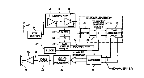
5 FIG. 1 is a block diagram of a radio receiver according to one
embodiment of the present invention.
FIG. 2 is a block diagram of a radio receiver according to another
embodiment of the present invention.
FIG. 3 is a block diagram of a radio receiver according to still
1o another embodiment of the present invention.
DETAILED DESCRIPT10N
Referring to FIG. 1, a block diagram of a radio receiver 10
according to one embodiment of the present invention is shown. The radio
receiver 10 receives an RF signal via an antenna 12 and applies it to an RX/IF
section 14. The received RF signal is suitably modulated with information
transmitted from an information source. In an exemplary embodiment, the RF
signal is modulated with coded audio information transmitted from a~radio
transmitter (not shown) operated by a user transmitting voice messages to
the radio receiver. The RF/1F section 14, which provides receiver selectivity,
down converts the RF signal to provide an IF signal with a predefined
intermediate frequency, on line 1 fi.
In an exemplary embodiment, the received RF signal is a CDMA
signal having a chip rate of 1.2288 MHz that complies with the
Telecommunication Industry Association (TIA) Interim Standard 95 (IS-95
standard). Preferably, the intermediate frequency is selected to be six times
the chip rate. For the reasons explained in the background section, it would
be appreciated that producing the I and Q components of such wide band IF
3 o signal according to the conventional method requires an extremely high
CA 02297734 2000-O1-24
' WO 99/05781 . PCT/US98l14093
6
sampling rate, to produce a phase signal with adequate resolution. For
example, for a conventional phase detector that, relative to a reference
signal,
provides a 30 degree phase resolution, the timing of zero crossings must be
1
made with a clock of 72 times the chip rate, or about 100 MHz. As described
later in detail, instead of determining the phase of the limited 1F signal,
the
radio receiver 10 generates normalized I and Q components by sampling a
normalized IF signal at a much lower rate of about 8 times the chip rate, or
about 10 MHz. The present invention then combines the normalized I and Q
components with the amplitude of the IF signal to produce the I and Q
1o components of the complex baseband signal.
According to the present invention, the 1F signal provided by the
RFIIF section 14 is applied to a limiting amplifier 18. The limiting amplifier
18
includes a predetermined number of cascaded amplifier stages 19, with each
stage having a predefined gain. The gain of the amplifier stages 19 ace
selected such that stronger IF signals saturate early amplification stages,
and
weaker IF signals saturate the subsequent amplification stages 19. As a
result, the limiting amplifier 18 produces a normalized 1F signal that has a
square wavefocm. According to the embodiment shown in FiG. 1, the
normalized IF signal is applied to an analog filter 20 to remove its high
2 o frequency contents. Consequently, the analog filter 20, which may be a
band
pass or a low pass filter, converts the square waveform of the normalized IF
signal into a sinusoidal signal that contains the phase information of the
modulated received signal.
The sinusoidal normalized IF signal at the output of the analog
filter 20 is applied to a complex sampling circuit 22 that includes a
quantizer
24 that provide numerical representation of the normalized I and Q
components. One such complex sampling circuit is described in U.S. Patent
No. 4,888,557 issued to Puckette et al., which is hereby incorporated by
reference. Using a clock circuit 21, the complex sampling circuit 22 samples
the normalized IF signal at a sampling rate substantialiy equal to 4/(2n + 1 )
CA 02297734 2000-O1-24
WO 99/05781 PCT/IJ898/14093
7
times the intermediate frequency, where n is an integer equal to or greater
than zero. In the preferred embodiment, the sampling rate of the normalized
IF signal is selected to be 4/3 times the intermediate frequency, or 8 times
the
chip rate. The complex sampling circuit 22 samples the normalized IF signal
in a staggered manner such that the quantized and normalized f and Q
samples are interleaved. The quantized normalized I and Q samples may
include alternate I and Q samples that are negated with respect to. each
other.
For example, the output of the complex sampling circuit may be a sequence of
1, -Q (Q bar), -I(I bar), and Q. The present invention adjust for the negated
I
l0 and Q samples during a subsequent interpolation stage.
The outputs of the quantizer 24 are applied to an alignment
circuit 26 for aligning the interleaved normalized f and Q components with
each other. The alignment circuit 26 may be an interpolation circuit that
aligns the I and Q components by performing a well known interpolation
technique. A simple interpolation technique combines two consecutive
normalized I components and two consecutive normalized Q components, to
compute an 1 and a Q value at the middle of the center two values, thus time-
aligning the interleaved I and Q components with each other. In this way, the
output of the alignment circuit 26 comprises the normalized I and Q
2o components of the received signal referenced relative to a common instant
in
time. As explained above, the time alignment circuit adjust for the negated I
and Q samples, as welt. Accordingly, the filter 20, the complex sampling
circuit 22, and the alignment circuit 26 constitute a quadrature circuit 27
that
produces the normalized I and Q components of the normalized IF signal.
. At each amplification stage 19, the limiting amplifier 18 includes
a number of amplitude detectors, such as diodes 28, that produce a DC signal
representing the signal amplitude at the output of a corresponding stage. The
outputs of the detectors are summed with each other in a well known
manner, to produce a received signal strength indicator (RSSI) signal on fine
30, which is a logarithmic~representation of the received signal amplitude.
CA 02297734 2000-O1-24
WO 99/05781 PCT/US98/14093
8
The RSSI signal is applied to a sarnpler/quantizer circuit 32 that, using the
clock 21, also samples it at 8 times the chip rate to provide a numerical
representation of the received signal at each sampling instance. Because the
dynamic range of the RSSI signal may be high, a large number of bits would
be needed to represent the quantized RSSI signal, resulting in high power
consumption. In order to lower the power consumption, a filter 31 is added
before the quantizer 32. The filter 31 essentially performs a differencing
operation relative to consecutive samples. Since the RSSI does not change
very significantly over short intervals of time (fractions of a bit period),
the
1o filter 31 provides an RSSI signal with low dynamic range, which can be
quantized with fewer bits.
The quantized RSSI signal, on line 41, is applied to an AGC
circuit 36 to provide a modified RSSI signal on line 38. The AGC circuit can
re-integrate the RSSI values to compensate for the differencing filter 31. An
exemplary AGC circuit 36 performs a substraction of a slowly adapted value
from the quantized RSSI signal to maintain it within a desired range. The
subtracted value is adapted based on the total power received in the IF
bandwidth due to a sum of CDMA signals.
The modified RSSI signal and the normalized I and Q components
2o are applied to a combiner circuit 40 that combines the normalized I and Q
components with their corresponding quantized amplitude samples, to provide
the I and Q components of the complex baseband signal. In an exemplary
embodiment, the combiner circuit 40 includes a lookup table that combines
the modified RSSI signal with the normalized I and Q components by
outputting a numeric representation that corresponds to the multiplication of
the normalized I and Q components by their corresponding RSSI amplitude
samples.
The numerically represented I and Q components are applied to a
DSP 42 to retrieve the coded audio information using a suitable demodulation
data processing technique. The coded audio information is applied to a codec
CA 02297734 2000-O1-24
WO 99/05781 PCT/L1S98/14093
9
44 for decoding the coded audio information according to the coding
technique used when transmitting the audio information. The codec 44
provides an audio signal on line 46 representing the transmitted audio. The
audio signal is applied to an audio amplifier 48, which amplifies the audio
signal and presents it to a speaker 50, for rendering an audible sound of the
transmitted voice messages.
Referring to FIG. 2, another embodiment of the radio receiver 10
of the present invention is shown. Similar to the embodiment of FIG. 1, the
received RF signal, after being converted to the IF signal, via the RF/lF
section
l0 14, is normalized by the limiting amplifier 18. Because the normalized (F
signal at the output of the limiting amplifier 18 has a square wave form, the
digital filter 52 uses a one bit quantization technique. Therefore, the
normalized IF signal is applied to a 1-bit analog to digital quantizer 51,
which
provides a sequence of binary states representing the normalized IF signal.
According to this embodiment of the invention, however, the output of the
quantizer 51 is applied to a digital filter 52 instead of the analog filter 20
of
FIG. 1. The digital filter 52 performs the task of removing high frequency
contents of the normalized 1F signal through well known digital filtering
techniques. The digital filter 52 samples thenormalized IF signal, to achieve
2o a desired accuracy in producing the sinusoidal representation of the
normalized 1F signal. After being digitally filtered, the normalized signal is
applied to a sub-sampling circuit 53, which depending on the sampling rate
selects sub-samples of the normalized IF signal for providing.the normalized I
and Q components. Thereafter, the normalized I and Q components are
processed according to the present invention as described in connection. with
F1G. 1. Filter 52 may alternatively be a hybrid analog/digital filter, in
which
the signal is partly analog filtered and then digitized as a ternary (1, 0, -
1)
sample or to a sample of two bits accuracy. The coarsely quantitized sample
is then digitally filtered, thus completing a hybrid filtering operation.
CA 02297734 2000-O1-24
WO 99/05781 . PCT/US98/14093
Although a logarithmic amplifier, as incorporated in the limiting
amplifier 18, can be made to have an adequate dynamic range, if the amplifier
has more than about 50dB gain it is desirable to split it into gain blocks,
with
bandpass filters between the blocks in order to limit wideband noise
5 accumulation. The filters then introduce delay such that the detected signal
from later detector stages is delayed compared to the detected signal from
earlier stages. U.S. Patent No. 5,070,303~to Dent, which is hereby
incorporated by reference, discloses delaying the detected signal from earlier
stages to time-align it with that of later stages before combining.
1o Referring to FIG. 3, yet another embodiment of the invention is
shown, which uses a feedback AGC to limit dynamic range so that only one (F
filter and RSSI amplifier stage is needed, thus avoiding time-alignment to
compensate for filter delay. This embodiment is envisaged primarily for
continuous reception as when using CDMA. !n FIG. 3, the limiting amplifier
includes a logarithmic amplifier 63, which is assumed to have lower dynamic
range than the total range of signal levels that may be received. Also, under
this embodiment, an AGC amplifier 60 and an IF filter 61 are coupled between
the RF/IF section 14 and the logarithmic amplifier 63.
The AGC amplifier 60 enables the signal level presented to the
2o logarithmic amplifier 63 to be controlled to an optimum region. An AGC
circuit 62 detects whether the RSSI signal from the logarithmic amplifier 63
is
greater or less, on average, than the optimum value and applies a control
signal to the AGC amplifier 60 accordingly to adjust the signal level toward
the optimum vatue. The AGC is relatively slow in operation compared to the
signal bandwidth; the stability of this AGC feedback loop is therefore not
impaired by inclusion of the IF filter 61 within the AGC loop.
Thus, the wideband gain, defined as the gain of the logarithmic
amplifier 63 between the output of the IF filter 61 and the input to the
complex sampling circuit 22 may be reduced to prevent build-up of wideband
3 0 noise in the logarithmic amplifier 63.
CA 02297734 2000-O1-24
WO 99/05781 PCTIUS98/14093
11
Despite the slowness of the .feedback AGC, it is desirable to
compensate for its action and thus the AGC circuit 62 preferably first
compensates the RSSI signal for the amount of gain reduction applied to the
AGC amplifier 60 before reporting the true RSSI for further processing
circuitry. The so-compensated RSSI signal is then digitally scaled by means
of the aforementioned combination with a slowly adapted constant in order to
produce a scaled, digitized amplitude signal to the combiner 40.
The Combiner 40 combines the scaled amplitude signal sample-
by sample with the time-aligned, normalized I,Q values from the time
to alignment circuit 26 in order to re-insert amplitude information into.the
I,Q
values prior to digital signal processing by the DSP 42 to decode the CDMA
signal, using for example a RAKE receiver. Using the arrangement of FIG. 3,
it is possible to omit the use of the logarithmic amplifier 63 and instead use
a
linear arnplifierldetector. This is possible when the feedback AGC may be
relied upon to maintain a relatively constant total signal level at the input
of
the amplifier. If a linear amplifier is used for amplifier 63, in which
instantaneous amplitude variations of the signal are not erased and pass
through to combiner 40, it may not be necessary to re-insert the amplitude
information removed by the feedback AGC circuit before decoding.
2o Nevertheless, the effect of the feedback AGC on the signal level is still
preferably combined with the amplitude information preserved on the I,Q
signals in order to determine the true signal strength received. The true
signal
received is useful to know when comparing alternative sources of a received
signal and deciding which source (e.g., base station) to prefer for receiving
2 S service.
From the foregoing description of the embodiments of the
invention it wilt be appreciated that the present invention does not require
detection of the phase of the normalized IF signal, thus, eliminating the need
for a high frequency clocking circuit. In this way, the present invention
3 o provides a simple method for producing complex baseband signals that are
CA 02297734 2000-O1-24
WO 99/05781 PCT/US98/14093
12
derived from a wideband received signal. As a result, the wideband radio
receiver of the invention can cost effectively process the RF received signals
without consuming substantial current.
Although the invention has been described in detail with
reference only to the presently preferred embodiment, those skilled in the art
will appreciate that various modifications can be made without departing from
the invention. Accordingly, the invention is defined only by the following
claims which are intended to embrace all equivalents thereof.