Note: Descriptions are shown in the official language in which they were submitted.
CA 02298428 2000-04-19
WH-10,757CA
TITLE: BATTERY CHARGING CIRCUIT
FIELD OF THE INVENTION
The present invention relates to battery charging
circuits, and in particular, to a battery charging circuit
having a high power factor.
BACKGROUND OF THE INVENTION
Recent advances in rechargeable batteries have
greatly extended the number of products which can be
powered by a relatively small battery. In many of these
products it is desirable to have a charging circuit
associated with the product to allow convenient recharging
of the battery. As most of these devices are portable,
weight and size of the charging circuit are important
factors, and from a marketing point of view, the cost of
the circuit is also important.
The growth of rechargeable battery operated devices
have also forced utilities to reconsider specifications for
charging circuits as many of the early designs had
relatively poor power factor corrections. As the number of
products increase, this has become a concern for the
utilities and thus, the specification, with respect to
recharging circuits is changing.
Switching power supply devices of a type without
power factor correction have been used. These devices
rectify an AC voltage and process the rectified AC voltage
using a bulk holdup capacitor to smooth it to a DC voltage.
This smoothed DC signal is then provided to a flyback
transformer circuit which is controlled by a switch.
Feedback is provided from the charging current of the
secondary winding and the feedback circuit is relatively
fast to maintain a desired, instantaneous charging current.
- 1 -
CA 02298428 2000-02-10
WH-10, 75.7CA
The smoothing of the rectified AC signal has the
advantage that the signal provided to the primary winding
for powering thereof is more constant, and thus, the
charging current provided by the secondary winding is more
consistent. The charging current may be closely monitored
and fast correction of variations in the charging current
is provided by the feedback mechanism and a control
arrangement associated with the switch of the flyback
transformer. Unfortunately, this design has a relatively
poor power factor. In addition, the design includes a
number of bulky and expensive components for smoothing of
the input signal which further increases the cost of the
charging circuit.
The present invention provides a simplified circuit
which has desirable characteristics with respect to
achieving a predetermined power factor, has improved space
utilization, and is cost effective.
SUMMARY OF THE INVENTION
A battery charging circuit according to the present
invention comprises means for receiving an AC input signal,
means for rectifying the AC input signal to produce a non
constant DC signal and providing said non constant DC
signal to an input of a flyback transformer circuit. The
flyback transformer circuit comprises a primary winding in
series with a switch, and a secondary winding associated
with said primary winding, and having a diode. The
secondary winding produces a current for charging of a
battery. A control arrangement controls the opening and
closing of the switch and thereby defines a time on and
time off of the switch. The control arrangement controls
the time on as required to meet a predetermined power
factor specification.
- 2 -
CA 02298428 2000-02-10
WH-10,757CA
The charging circuit of the invention recognizes
that the rectified AC signal can advantageously be used for
powering of the primary winding without any extensive
smoothing of the signal. Such smoothing of the signal
typically has been accomplished in prior art devices using
a large, relatively expensive bulk holdup capacitor.
With the present invention, the time on is
controlled to achieve or meet a predetermined power
specification. The time on, in some applications, can be
constant or where it is desired to vary the time on to
appropriately increase or decrease the charging current,
the time on is varied slowly and thus, high power factor
correction is possible.
The present invention recognizes that the input
signal to the primary winding can vary, and the resulting
charging current for charging of the battery can vary in
each cycle, and that satisfactory charging of the battery
is possible. The battery is quite tolerant to variation in
the charging current. In most cases, the charging current
only need to be controlled to not exceed some maximum
level. Therefore, the time on can be set to achieve a
desired maximum current for the maximum voltage provided by
the input signal. By controlling the time on to achieve
the acceptable characteristics for the charging current,
effective charging of the battery can occur. The charging
circuit of the present invention is quite simple in design
and has relatively few components. This combination is
space efficient, weight efficient, and has a controllable
power factor correction. This is also highly desirable for
portable products.
A battery charging circuit according to an aspect
of the invention, has the control arrangement control the
rate of change of time on to meet the predetermined power
factor specification.
- 3 -
CA 02298428 2000-02-10
WH~10, 75~7CA
According to yet a further aspect of the invention,
the circuit includes an input arrangement for entering a
battery charging specification and the control arrangement
varies the time on to meet the battery charging
specification. Typically, the specification can be set
according to the maximum charging current relative to
voltage of the battery and these conditions can be
monitored to meet the charging specification.
A battery charging circuit according to the present
invention has the rectified AC signal applied directly to
the primary winding and this signal continuously varies
from 0 volts to a maximum voltage and the charging current
produced by the secondary winding continuously varies as a
function of the rectified AC signal.
A battery charging circuit according to an aspect
of the invention allows for considerable variation in the
instantaneous charging current and this charging current
can vary at least 25 per cent during each cycle. The
changing current can be smoothed if desired by processing
after the secondary winding.
According to yet a further aspect of the invention,
the rectified AC signal used to power the primary windings
pulses and the battery charging current produced by the
secondary winding varies as a function of the rectified AC
pulsating signal.
The battery charging circuit of the present
invention is advantageously used in combination with the
charging of different types of batteries, including nickel
cadmium batteries or lithium batteries.
BRIEF DESCRIPTION OF THE DRAWINGS
Preferred embodiments of the invention are shown in
the drawings, wherein:
- 4 -
CA 02298428 2000-04-19
WH-10,757CA
Figure 1 shows a simplified charging circuit;
Figure 2 is a schematic of a simplified charging
circuit with some additional components; and
Figure 3 shows various signals of the signal.
DETAILED DESCRIPTION OF THE PREFERRED EMBODIMENTS
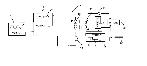
The battery charging circuit 2 of Figure 1 receives
an AC input signal at 4 and rectifies the AC signal at 6 to
produce a pulsating rectified AC signal generally shown at
7. This signal is provided to a flyback transformer
circuit comprising the primary winding 10, the controlled
switch 14, the secondary winding 24, and the current
rectifying diode 16. The secondary winding 24 provides a
charging current for the rechargeable battery 30. This
battery can be a lead acid battery, a nickel cadmium
battery or a lithium battery or other rechargeable battery.
A feedback arrangement 29 preferably provides
feedback with respect to the present voltage of the battery
as well as the charging current. This information can be
provided to the control arrangement 18. The control
arrangement opens and closes switch 14 in a predetermined
manner and defines an on time of the switch (Ton),
indicated as 19, and an off time of the switch (Toff)
indicated as 21. The on time charges the primary winding
and is discharged during the off time. This is the typical
operation of the flyback transformer.
The rectified AC signal has a frequency of
approximately 120 Hz and the switch 14 is opened and closed
at a rate at least 10 times this frequency. The control
arrangement 18 can vary the charging current provided to
the battery 30 by varying the on time. In order to provide
a high power factor, the rate of change of time on is slow
relative to the rectified AC signal 7. A very high power
factor close to unity can be obtained if the rate of change
of time on is 25 Hz or less, and preferrably, 12 Hz or
- 5 -
CA 02298428 2000-04-19
WH-10,757CA
less. This slow rate of change of Ton is quite acceptable
for charging of the battery 30.
As can be seen from the circuit of Figure 1, the
traditional flyback transformer and charging circuit, does
not include a bulk hold capacitor nor an in rush resistor
to smooth the DC signal that is provided to the primary
winding 10. This modification of the circuit significantly
reduces the cost of the circuit due to a reduction in
relatively expensive components and also allows for the
improved power factor.
The feedback arrangement 29 for some application
may provide very little feedback, if any. For example, for
some battery applications, it may be sufficient to use a
constant Ton such that the battery 30 is exposed to the
same current throughout the charging cycle. The charging
cycle can be stopped once the battery achieves a
predetermined voltage. For other applications, it will be
desirable to have a battery charging profile. Such
profiles are desirable with some nickel cadmium batteries,
as well as lithium batteries. In this case, a
predetermined battery charging profile can be provided to
the control arrangement 18 as indicated by the profile 32.
Such a profile can be a battery voltage relates to maximum
charging current relationship and the control arrangement
18 can vary Ton relatively slowly to on average, achieve a
desirable charging current. In this way, the maximum
charging current is maintained below a certain level.
It can be appreciated from the circuit of Figure 1
that the pulsating signal provided to the primary winding
10 will result in a pulsating charging current for charging
of the battery. Some smoothing of that charging current
can be provided if desired on the secondary side, however,
for most battery applications, this is not necessary. In
any event, the recognition that the pulsating input current
to the primary winding 10 is satisfactory allows vast
- 6 -
CA 02298428 2000-04-19
WH-10,757CA
improvement in the power factor, excellent control of the
charging characteristics of the battery, reduction in costs
of the circuit due to fewer components, as well as reduced
space requirements due to lesser components.
The charging circuit 2a of Figure 2 merely includes
some additional components but basically operates in the
same manner as Figure 1. On the input side, a small
capacitor 31 has been provided to eliminate high frequency
noise signals caused by the opening and closing of the
switch 14. This is not a bulk hold capacitor. It merely
prevents the high frequency signal being fed back to the
power system. The primary side of the circuit has also
been modified to include a circuit branch 33 across the
switch 14 which acts as a clamp for flyback protection of
switch 14 protecting it against over voltage.
The circuit of Figure 2 also shows an auxiliary
power arrangement 41 used to provide power to the control
arrangement 18. On the battery side of the circuit, a
battery filter arrangement 43 is shown which can modify and
smooth the charging current to the battery 30, if
necessary. A feedback arrangement 29 is also provided.
The simplified charging circuit of Figures 1 and 2,
has particular application for applications up to 250 to
300 watts. This power limitation is primarily determined
by the availability of suitable components for the circuit
at reasonable costs. If there is an application for higher
power requirements, rather than increasing the circuit
components, it may be preferrable to parallel the design.
The power factor is easily controlled as the rate
of change of Ton necessary to achieve a particular charging
of a battery is quite tolerant, and thus the feedback
arrangement can be slow, relative to the input signal.
This allows an average or dampened feedback response and
avoids wide variations in Ton. Most of the
CA 02298428 2000-04-19
WH-10,757CA
benefits with respect to the power factor correction have
been achieved due to the elimination of the in rush
resistor and the bulk hold capacitor of the traditional
flyback transformer charging circuit.
Basically, the design accepts the pulsating DC
signal provided to the primary winding and if necessary or
desired, suitable filtering of the charging current can
occur on the secondary side of the circuit.
It can fully be appreciated that the electronic
power switch shown as 14 can be any of the traditional
devices such as bi-polar transistor mosfet transistor, IGBT
transistor, etc. The circuit design of Figures 1 and 2,
allows for variation of the duration of Ton, however, any
changes therein are relatively slow. This, to a large
extent, provides the circuit with a generally constant duty
signal. The power factor specification is met by slowly
varying any change in Ton. Basically, Ton is constant as
the input signal to the primary winding varies from one
minimum through a maximum, to the next minimum. In fact,
in the preferred embodiments, Ton would not change for
several cycles of this signal. Ton can also be controlled
by distinct steps and is general constant between steps.
_ g
CA 02298428 2000-04-19
WH-10,757CA
The transferred power to the battery generally
follows the following equation.
(Vin*Ton)2*Frequency
Battery Power Out = ------------------------
2* (Primary Inductance of T1)
Where:
* means multiply
Vin is the instantaneous voltage across T1 and the
Electronic Switch
Ton is the on time, in seconds
Frequency is the frequency of the electronic switch operation in
Hertz
Primary Inductance of T1 is the primary inductance of T1
Battery Charger Power Out is the power delivered to the
battery ignoring losses
When Vin, the instantaneous rectified line voltage
is integrated over one complete line cycle, the output
power of the charger is
Battery Charger Power Out = (Line Voltage in rms)2* Constant
The power factor correction will occur so long as
the duty of the control circuit maintains nearly a constant
duty when averaged over one half cycle of the AC input line
voltage.
The output filter circuit of the flyback converter
is designed to reduce as required the output ripple current
as seen by the battery being charged. It can be nothing, a
filter capacitor, combination of passive devices or may
even include some form of active electronic circuit. The
feedback circuit monitors the charging of the battery,
sends a signal back to the electronic switch control
circuit and adjusts the duty to increase or decrease the
output power delivered to the battery.
_ g -
CA 02298428 2000-04-19
wH-10,757CA
The operation of the charging circuit has been
described with respect to a feedback arrangement where Ton
is slowly varied relative to the input signal. It is also
possible to vary the frequency of the switch 14 to thereby
vary the charging current for the battery. It is also
possible to use a combination of the variation of the
frequency and the variation of Ton to achieve a desired
charging characteristic. Varying the time on of the switch
is more traditional and easier to accomplish, and as such,
is the preferred control.
Modulation of time on or the switching frequency
will result in the modulation of the input source current,
thereby degrading the power factor.
If time on and frequency are held constant, a high
power factor (better than .93) in practical implementation
of the circuit is achieved. Power factors of better than
.80 are easily obtained with slow modulation of time on or
switching frequency.
In many cases, the switch 14 will operate at a
frequency in the order of 100 KHz. The feedback for
variation of Ton is preferrably of the order of 10 Hz. It
is also possible to have different profiles for Ton that
vary as a function of time. The important thing is that
Ton over a number of cycles of the input signal does not
widely vary and as such, a high power factor power is
achieved. If certain applications do not require a high
power factor correction, then the rate of change of Ton can
approach the frequency of the input signal. Therefore, the
rate of change of time on and/or frequency of the switch is
controlled to meet a particular power factor specification.
Figure 3 shows various signals of the circuit.
- 10 -
CA 02298428 2000-04-19
WH-10,757CA
The charging circuit has been described with
respect to charging a battery, however, the circuit can be
used for other applications which can accept the output
waveform of this circuit directly or modified on the
secondary side of the circuit.
Although various preferred embodiments of the
present invention have been described herein in detail, it
will be appreciated by those skilled in the art, that
variations may be made thereto without departing from the
spirit of the invention or the scope of the appended
claims.
- 11 -