Note: Descriptions are shown in the official language in which they were submitted.
CA 02298473 2000-O1-21
r
DATA CARRIER WHICH CAN BE OPERATED WITHOUT CONTACT
This invention relates to a data carrier having an integrated circuit and at
least
one insulating supporting substrate on which a transfer element is disposed
for trans-
ferring data to an external device, and to a method for producing such a data
carrier.
A data carrier of the abovementioned kind is known from EP 0 756 244 A2
whose disclosure is taken as a basis for the further description. EP 0 756 244
A2
describes a circuit unit having an insulating supporting substrate on which a
conduc-
tive flat coil is located. The coil can consist of a plurality of coil layers
separated by
insulating layers. In order to interconnect the individual coil layers into a
coil, each
of the insulating layers has at least one hole. The coil ends can be connected
with an
integrated circuit or an electronic module containing the integrated circuit
solely if
the coil ends touch the terminals of the integrated circuit or the contacts of
the mod-
ule. The individual turns of the coil can be so disposed and dimensioned that
the
circuit unit is embossable without restriction within an area specified by the
stan-
dard.
It is especially important for perfect operation of the data carrier that the
elec-
tric connection between the transfer element, which can be formed for example
as a
coil, and the integrated circuit, which is optionally mounted in the data
carrier in the
form of an electronic module, be reliable throughout the life of the data
carrier.
It is therefore the problem of the invention to design the structure of the
data
carrier in such a way as to ensure a lastingly reliable electric connection
between the
transfer element and the integrated circuit or electronic module.
This problem is solved by the feature combinations of the independent claims.
The essential aspect of the invention is that the data carrier is formed so as
to
permit double-sided contacting, i.e. contacting of both main faces of the
integrated
circuit or the electronic module containing the integrated circuit, with the
transfer
element.
This manner of contacting has the advantage of eliminating the effort of a sol-
dering process or of metering conductive adhesive for contacting, while
nevertheless
achieving a very reliable and long-lived electric connection between transfer
element
CA 02298473 2000-O1-21
-2-
and electronic module or integrated circuit. Whenever the contacts of the
integrated
circuit or electronic module come away from the transfer element on one side
as a
result of bending stress or other effects, thereby worsening the electric
connection,
the exactly opposite effect occurs on the other side of the integrated circuit
or elec-
tronic module so as to compensate the adverse effects. The described motion
causes
the transfer element to be pressed against the contacts of the integrated
circuit or
electronic module on the opposite side of the integrated circuit or electronic
module,
so that the electric connection between integrated circuit or electronic
module and
transfer element is at least not clearly worsened or even improved. This
ensures that
the electronic data carrier still works reliably even upon strong bending
stress.
Furthermore, regardless of the cause for detachment of the transfer element
from one or more contacts of the electronic module or integrated circuit, the
redun-
dant design of the connecting points reduces the risk of a resulting
disruption of
service. The described compensation or redundancy effect presupposes, however,
that the electronic module or integrated circuit used has contacts which are
accessi-
ble from both main faces, or two sets of contacts which are redundant relative
to
each other, one set being disposed on each main face. This is already the case
in
particular with so-called lead-frame modules wherein the integrated circuit is
dis-
posed on a thin metal frame. The invention can therefore be used especially
advan-
tageously in conjunction with lead-frame modules.
However, the invention also offers advantages with electronic modules or inte-
grated circuits which are only contactable via one of the two main faces. In
this case
one also gains an additional degree of freedom for producing the data carrier
since
the transfer element is contactable in different mounting positions of the
electronic
module or integrated circuit.
A further advantage of the invention is that, starting out from the data
carrier
known from EP 0 756 244 A2, the above-described improvement of the electric
con-
nection between transfer element and integrated circuit or electronic module
can be
obtained by the relatively simple measure of double-sided contacting, which
can be
realized without introducing a new technique into the production process and
thus
hardly increases production costs.
CA 02298473 2000-O1-21
-3-
The transfer element is preferably printed on insulating layers of the data
car-
rier in the form of a coil, the screen printing technique being especially
well suited.
The invention will be explained below with reference to the drawings. A chip
card is selected here as an embodiment for the data carrier, and a printed
coil for the
transfer element. The data carrier can of course also be designed differently
and be
integrated for example into a key or another object of daily use. For the
transfer ele-
ment one can also use an electrostatic coupling surface for example.
Fig. 1 shows an embodiment of the inventive chip card wherein the integrated
circuit is embedded in the card body in the form of an electronic module, in a
plan
view,
Fig. 2 shows a further embodiment of the inventive chip card wherein the inte-
grated circuit is embedded in the card body directly, in a plan view,
Fig. 3 shows a layer structure of the chip card shown in Fig. 1 before lamina-
tlon, In cross section along line A-A,
Fig. 4 shows the chip card shown in Fig. 1 in cross section along line A-A,
Fig. 5 shows a layer structure of the chip card shown in Fig. 2 before lamina-
tion, in cross section along line A-A, and
Fig. 6 shows the chip card shown in Fig. 2 in cross section along line A-A.
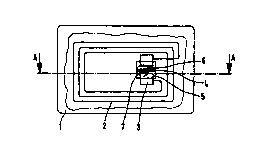
Fig. 1 shows an embodiment of the inventive chip card wherein the integrated
circuit is packed in an electronic module, in a plan view. Chip card 1 is
designed for
noncontacting data exchange with an external device and fulfills ISO standard
7810
with respect to its outer dimensions. Within an area limited by a wavy line
one sees
a view of the inner structure of chip card 1. For clarity's sake the
individual card lay-
ers are not shown but rather only the components embedded in or between the
lay-
ers. These components consist in particular of coil 2 whose ends 3 are greatly
wid-
ened in order to establish an optimal electric contact with electronic module
4 in
which integrated circuit 7 is embedded. Integrated circuit 7 is covered by
casting
body 6 and electrically connected with contact surfaces 5 of electronic module
4.
Electronic module 4 is preferably formed as a lead-frame module wherein
metallic
contact surfaces 5 serve as a supporting substrate for integrated circuit 7
together
with casting body 6. Contact surfaces 5 are each electrically connected with
widened
CA 02298473 2000-O1-21
-4-
ends 3 of coil 2 in each case. Further, the backs of contact surfaces 5 are
connected
with electroconductive surfaces 17, which are not visible in Fig. 1 since they
come
to lie under coil ends 3. Each of electroconductive surfaces 17 is in addition
con-
nected with one coil end 3.
Coil 2 including widened coil ends 3 as well as electroconductive surfaces 17
are preferably produced by printing technology. One produces the electric
connec-
tion between coil ends 3 or electroconductive surfaces I7 and contact surfaces
S by
connecting the individual layers constituting chip card 1 and carrying coil 2
or elec-
tronic module 4 into a card body by lamination, so that coil ends 3 or
electrocon-
ductive surfaces 17 and contact surfaces 5 now lastingly touch each other.
This
contact between coil ends 3 or electroconductive surfaces 17 and contact
surfaces S
can be established alternatively at a time when printed coil ends 3 or
electroconduc-
tive surfaces 17 are totally dried off or at a time when the drying process is
not yet
over. According to the invention, contact surfaces 5 are connected with coil
ends 3
on each side. As explained above, this cannot be seen in Fig. 1 since
electroconduc-
tive surfaces 17, which are connected with the back of contact surfaces 5,
come to
lie exactly under coil ends 3 shown and are therefore not visible. The
inventive con-
tacting technology is clearly recognizable in Figs. 3 to 6, however, and will
be de-
scribed in detail with reference to these figures.
Fig. 2 shows a further embodiment of inventive chip card 1 which differs from
Fig. 1 only in that integrated circuit 7 is not packed in electronic module 4
but em-
bedded directly in the card body. On its surface, integrated circuit 7 has
contacts 8
which are in touching connection with coil ends 3. As in Fig. l, coil ends 3
are addi-
tionally connected in the embodiment of Fig. 2 with electroconductive surfaces
17
which are again connected with contacts 8 disposed on the back of integrated
circuit
7.
Fig. 3 shows the layer structure of chip card I shown in Fig. I before lamina-
tion of the individual layers, in cross section along line A-A. In the
embodiment
shown in Fig. 3 chip card 1 consists of six individual layers. Electronic
module 4 is
disposed in layer 9 in such a way that contact surfaces 5 of electronic module
4
come to lie in a recess of layer 9 and casting body 6 protrudes beyond layer
9. On
CA 02298473 2000-O1-21
-5-
each side of layer 9 there are layers 10 and 11. Layer 10 carries printed coil
2 in-
cluding coil ends 3, whereby coil ends 3 come to lie opposite contact surfaces
S of
electronic module 4. Layer 11 is disposed on the side of layer 9 beyond which
cast-
ing body 6 protrudes and contains recess 12 for receiving casting body 6.
Instead of
recess 12, layer 11 can also have a perforation completely penetrating layer
11.
Further, layer 11 carries electroconductive surfaces 17 which can be
electrically
connected with coil ends 3 disposed on layer 10 via at least one plated-
through hole
13 in layer 9. Toward the outside of the card, layer 11 is followed by another
layer
14 and finally cover layer 15. Layer 10 is followed toward the outside of the
card by
cover layer 16. The layer structure can vary within wide limits depending on
the area
of use. In particular one can dispense with cover layers 1S and 16 or layers
10 and
14. All layers can consist of the materials customarily used in chip cards,
for exam-
ple PVC, ABS, PETG, polycarbonate, etc.
Fig. 4 shows chip card 1 shown in Fig. 1 in cross section along line A-A. Chip
card 1 shown in Fig. 4 was produced by laminating the stack of single layers
shown
in Fig. 3. Before the layers are stacked they are provided with the components
shown in Fig. 3, such as coil 2 together with widened coil ends 3,
electroconductive
surfaces 17, plated-through holes 13 and electronic module 4. Fig. 4 clearly
shows
the inventive double-sided contacting of contact surfaces S of electronic
module 4
through coil ends 3 and electroconductive surfaces 17. The electric connection
be-
tween coil ends 3 and contact surfaces S is established by the laminating
process.
Coil ends 3 are thereby pressed against the upper side of contact surfaces S,
and
electroconductive surfaces 17 are electrically connected with coil ends 3 by
at least
one plated-through hole 13 in each case and pressed against the lower side of
contact
surfaces S. This procedure achieves double-sided contacting of contact
surfaces S so
that a reliable electric connection between coil 2 and integrated circuit 8 is
ensured
even when coil ends 3 are detached from contact surfaces S for example as a
result
of bending stress on chip card 1. In this case the electric contact is still
maintained
through electroconductive surfaces 17.
A fiurther effect of double-sided contacting is that one can use electronic
mod-
ules 4 of different constructions for chip card 1 shown in Fig. 4, it being
irrelevant
CA 02298473 2000-O1-21
-6-
whether contacting of electronic module 4 is possible only from the upper
side, only
from the lower side or on both sides. In case electronic modules 4 are only
contact-
able on one side, one of course does not have the advantage of higher
reliability of
the electric connection as with double-sided contacting. However, the card
structure
shown in Fig. 4 offers the advantage over conventional card structures with
one-
sided contacting that the card structure can be used for different electronic
modules
4 in an unchanged form.
Fig. S shows the layer structure of chip card 1 shown in Fig. 2 before lamina-
tion of the individual layers, in cross section along line A-A. The layer
sequence
corresponds to the layer sequence shown in Fig. 3 but layers 9 and 11 are
modified.
According to Fig. 5 layer 9 has hole 18 in which integrated circuit 7 is
embedded.
Further, layer 9 has at least one plated-through hole 13. In contrast to Fig.
3, layer 11
shown in Fig. 5 has no recess 12 and only carries electroconductive surfaces
17 dis-
posed opposite contacts 8 of integrated circuit 7 and opposite the at least
one plated-
through hole 13 in each case. Analogously to Fig. 3, layer 10 carries coil 2
and coil
ends 3 disposed opposite contacts 8 of integrated circuit 7 pointing in their
direction
and opposite the at least one plated-through hole 13 in each case.
Fig. 6 shows chip card 1 shown in Fig. 2, which was produced by laminating
the layer stack shown in Fig. 5, in cross section along line A-A. The
laminating
process causes coil ends 3 to be pressed against the at least one plated-
through hole
13 in each case and against contacts 8 of integrated circuit 7 facing them,
thereby
creating electroconductive connections. On the opposite side of layer 9
electrocon-
ductive surfaces 17 are pressed against contacts 8 of integrated circuit 7
facing them
and against the at least one plated-through hole 13 in each case, so that
electrocon-
ductive connections likewise arise here. Altogether, lamination causes coil
ends 3 to
be connected with electroconductive surfaces 17 via the at least one plated-
through
hole 13, and both coil ends 3 and electroconductive surfaces 17 to be
electrically
connected with contacts 8 of integrated circuit 7 facing them in each case.
In the embodiment of inventive chip card 1 shown in Fig. 6, double-sided con-
tacting also, on the one hand, has the effect of low sensitivity to bending
stress or
other stresses which may lead to contact problems and, on the other hand,
offers a
CA 02298473 2000-O1-21
-7-
universal mounting possibility for integrated circuit 7 which can also carry
contacts
8 on only one side and can then alternatively be mounted so that contacts 8
point
toward layer 10 or toward layer 11.
The layer sequence shown in the described embodiments is to be regarded as
only one of many possibilities. Thus, any other layer structures can similarly
be used
for realizing the inventive idea. The essential thing is that double-sided
contacting of
electronic module 4 or integrated circuit 7 is possible or that, as an
alternative
thereto, electronic modules 4 or integrated circuits 7 having contact surfaces
5 or
contacts 8 on only one side can alternatively be mounted in such a way that
contact
surfaces 5 or contacts 8 point alternatively to one or the other main face of
the chip
card.
Coil 2 ca.n also be applied alternatively to a single layer on one or both
sides or
be distributed over a plurality of layers.
In a modification of the invention, coil 2 is applied partly to layer 10 and
partly
to layer 11. The two coil parts are interconnected through at least one plated-
through
hole in layer 9. Layers 10 and 11 each carry one coil end 3 and one
electroconduc-
tive surface 17 which is connected with coil end 3 of other layer 11 or 10 via
at least
one plated-through hole 13 in layer 9 in each case.
In a fiu~ther modification of the invention, at least part of coil 2, coil
ends 3
andlor electroconductive surfaces 17 is applied to layer 9 having electronic
module 4
or integrated circuit 7, whereby the arrangement of the individual components
in the
card can be retained.