Note: Descriptions are shown in the official language in which they were submitted.
CA 02298633 2000-O1-31
WO 99/63626 PCT/KR99/00266
-1-
ANTENNA CONNECTOR FOR RADIO COMMUNICATION EQUIPMENT
Technical Field
The present invention relates, in general, to an
antenna connector for radio communication equipment and,
more particularly, to an antenna connector provided with
an impedance transformer having a flat cutout portion, the
connector being also designed to control the bandwidth of
an antenna in accordance with the length of the antenna
and the number of turns of the antenna, or a helical
antenna, fitted over the impedance transformer and to
allow the bandwidth of the antenna to be easily and
simply controlled as desired.
Background Art
As well known to those skilled in the art, the
signal feed structure of conventional small-sized antennas
for radio communication equipment has been designed in
that a signal is directly fed to a coaxial line. Such a
signal feed structure includes two types: a monopole type
wherein a signal is fed to the plus portion of a coaxial
line, and a dipole type wherein a signal is fed to both
the plus and minus portions of a coaxial line.
However, the above-mentioned signal feed structure
for antennas is problematic in that it results in an
unbalance between signal feed lines of an antenna, thus
practically making it difficult to match the impedance of
the antenna. Such a signal feed structure also causes
the contact portions between the antenna and the signal
feed lines to be frequently changed, thus allowing the
characteristics of the antenna to be undesirably changed.
This results in a reduction in the antenna efficiency.
Fig. 1 shows the construction of a conventional wide-
band helical antenna disclosed in U.S. Patent No.
4,772,895. The above wide-band helical antenna is
designed to broaden frequency response and comprises a
feed port including a signal feed portion and a ground
portion. The above antenna also comprises two helically
CA 02298633 2000-O1-31
WO 99/63626 PCT/KR99/00266
-2-
configured conductive elements: first and second elements
200 and 400. The first element 200 has opposite ends,
and exhibits a first pitch and a first electrical length.
One end of the first element 200 is coupled to the signal
feed portion of the feed port . On the other hand, the
second element 400 has opposite ends, and exhibits a
second pitch and a second electrical length. The second
element 400 is coaxially wound around a portion of the
first element. One end of the second element 400 is
coupled to the ground portion of the feed port. The
second pitch is equal to approximately one half of the
first pitch, while the second electrical length is equal
to approximately one third of the first electrical length.
The above antenna further comprises a cylindrical spacer
means 300. The above spacer means 300 is coaxially
situated between the first and second elements 200 and
400, thus electrically insulating the two elements 200 and
400. The spacer means 300 is also sufficiently thin such
that the first element is tightly coupled to the second
element so as to broaden the frequency response exhibited
by the first element.
In the above wide-band helical antenna, the spacer
means, coaxially situated between the first and second
helical elements positioned inside and outside of the
antenna respectively, is used as a contact means for
allowing the two elements to be coupled together.
However, the above antenna is not designed to overcome
the unbalance between the signal feed lines experienced
in conventional antennas, thereby reducing the antenna
efficiency. Another problem associated with the above
wide-band helical antenna resides in that it is almost
impossible to make a small-sized antenna.
Disclosure of the Invention
Accordingly, the present invention has been made
keeping in mind the above problems occurring in the prior
art, and an object of the present invention is to provide
an antenna connector for radio communication equipment,
which converts the conventional parallel resonance of an
CA 02298633 2000-O1-31
WO 99/63626 PCT/KR99/00266
-3-
antenna into a series resonance by forming a flat cutout
portion on its impedance transformer, or the signal feed
part for the antenna, without changing the characteristics
of the antenna, thus broadening the bandwidth of the
antenna, and which easily and simply controls the
bandwidth of the antenna as desired by changing the size
and height of the impedance transformer, by changing the
surface area of the cutout portion of the impedance
transformer, or by changing the number of turns of the
antenna, or a helical antenna, fitted over the impedance
transformer.
Another object of the present invention is to provide
an antenna connector for radio communication equipment,
which is effectively used at various frequencies, thus
effectively and quickly meeting a variation of the central
frequency of an antenna with the variation being caused
by a change in environmental conditions of the antenna.
In order to accomplish the above objects, the present
invention provides an antenna connector for radio
communication equipment, comprising opposite ends, one end
of the connector being brought into contact with an
antenna and forming an impedance transformer part, and the
other end engaging with the radio communication equipment,
wherein the impedance transformer part comprises one or
more impedance transformers, at least one of the impedance
transformers being cut along a central axis thereof, thus
having a flat cutout portion. In the above antenna
connector, one or more flat cutout portions may be
partially or totally formed on the impedance transformer.
A longitudinal groove may be axially formed along a
central axis on each flat cutout portion of the impedance
transformer. In addition, two or more flat cutout
portions may be formed on the impedance transformer along
the central axis of the impedance transformer while being
spaced out at regular intervals. The above impedance
transformer may be separated from a locking boss of the
connector, with a coiled conductive wire being positioned
between the impedance transformer and the locking boss so
as to electrically connect the impedance transformer to
the locking boss. In the above antenna connector, two
CA 02298633 2000-O1-31
WO 99/63626 PCT/KR99/00266
-4-
flat cutout portions may be formed on the impedance
transformer in a way such that the two cutout portions
are positioned at opposite sides of one middle wall.
Brief Description of the Drawings
The above and other objects, features and other
advantages of the present invention will be more clearly
understood from the following detailed description taken
in con j unction with the accompanying drawings, in which
Fig. 1 is a perspective view of an antenna connector
in accordance with the primary embodiment of the present
invention;
Figs. 2a and 2b are perspective views of antenna
connectors in accordance with the second and third
embodiments of the present invention, respectively;
Fig. 3a is a graph, showing return loss as a
function of frequency for an antenna used with a
connector of this invention, with the center frequency of
the antenna being 315 MHZ, and Fig. 3b 'is a graph showing
both VSWR and impedance data as a function of frequency
for an antenna used with a connector of this invention,
with the center frequency of the antenna being 850 MHZ;
Fig. 4 is a perspective view of a conventional wide-
band helical antenna; and
Fig. 5a is a graph showing return loss as a function
of frequency for the antenna of Fig. 4, and Fig. 5b is a
graph showing both VSWR and impedance data as a function
of frequency for the antenna of Fig. 4.
Best Mode for Carrying Out the Invention
Figs. 1, 2a and 2b are perspective views of antenna
connectors in accordance with the primary to third
embodiments of the present invention, respectively. As
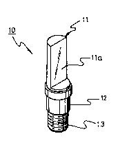
shown in Fig. 1, the antenna connector 10 according to
the primary embodiment of this invention comprises a
locking boss 12, which holds an antenna resonating at a
center frequency of a transmit and receive frequency band.
The connector 10 also has a connecting part 13 at which
CA 02298633 2000-O1-31
WO 99/63626 PCT/KR99/00266
-5-
the connector 10 engages with the connector holder of
radio communication equipment (not shown). The above
connector 10 further comprises a cylindrical impedance
transformer 11 or a signal feed part for the antenna.
The above impedance transformer 11 is cut along its
central axis, thus having a flat cutout portion lla.
Fig. 2a shows an antenna connector 10 according to
the second embodiment of this invention. In the antenna
connector 10 of the second embodiment, a groove llb is
axially formed along the central axis on the flat cutout
portion lla of the impedance transformer 11 in a way such
that the groove llb communicates with and is aligned with
a hole which is formed on both the locking boss 12 and
the connecting part 13.
Fig. 2b shows an antenna connector 10 according to
the third embodiment of this invention. In the antenna
connector 10 of the third embodiment, two flat cutout
portions lla are formed on the cylindrical impedance
transformer 11 while being spaced out at an interval.
Each of the two cutout portions lla is formed by a slit
14 having a semicircular cross-section.
The above antenna connector 10 of this invention has
the following operational effect. That is, a helical
antenna is fitted over the impedance transformer 11 and
is grounded to the antenna, with the antenna being
designed to resonate at a center frequency of a transmit
and receive frequency band. In such a case, the
conventional parallel resonance of the antenna is
converted into a series resonance by the impedance
transformer 11 or the signal feed part of the connector
10, thus broadening the bandwidth of the antenna at the
practical center frequency.
In a detailed description, when the resonance circuit
of an antenna exhibits a parallel resonance, the value Q,
or the quality factor of either a loss reactance element
or a resonance circuit, is substantially increased. This
finally and substantially reduces the bandwidth of the
antenna.
However, when the structure of the above antenna
connector 10 is converted into a distributed integer
CA 02298633 2000-O1-31
WO 99/63626 PCT/KR99/00266
-6-
circuit, thus allowing the input impedance, observed at
a signal feed point, to exhibit a series resonance, it is
possible to obtain a desired bandwidth at a wide
frequency band.
In an experiment performed to prove the operational
effect of this invention, a normal mode helical antenna
was used. Fig. 5a is a graph showing return loss as a
function of frequency for the conventional wide-band
helical antenna of Fig. 4. In the conventional helical
antenna of Fig. 4, the signal feed structure uses an I-
shaped engaging structure and uses a cylindrical contact
part having a diameter of 3 mm and a height of 10 mm.
In such a case, the antenna exhibits a bandwidth of about
8 MHZ at -20dB return loss as shown in Fig. 5a.
On the other hand, Fig. 3a is a graph, showing
return loss as a function of frequency for an antenna
used with the connector 10 of this invention, with the
center frequency of the antenna being 315 MHZ. In the
connector 10 of this invention, the impedance transformer
is formed by cutting a cylindrical body, having a
diameter of 3 mm and a height of 10 mm, along the central
axis of the cylindrical body, thus having a flat cutout
portion. The antenna, used with the connector 10 of this
invention, exhibits a bandwidth of about 20 MHZ at -20dB
return loss as shown in Fig. 3a.
As shown in Figs . 3a and 5a, the antenna, used with
the connector 10 of this invention and exhibiting a
center frequency of 315 MHZ, has a bandwidth which is
increased by about 250 relative to the center frequency.
Such an increase in the bandwidth of an antenna may be
expected in the case of a variety of linear antennas or
microstrip antennas in addition to such helical antennas.
Fig. 3b is a graph showing VSWR and impedance data
as a function of frequency for an antenna used with a
connector 10 of this invention, with the center frequency
of the antenna being 850 MHZ. In such a case, the
impedance transformer 11 of the connector 10 is formed by
cutting a cylindrical body, having a diameter of 5 mm and
a height of 2 mm, along the central axis of the
cylindrical body, thus having a flat cutout portion lla.
CA 02298633 2000-O1-31
WO 99/63626 PCT/KR99l00266
As shown in the drawing, the frequency bandwidth of the
antenna, used with the connector 10 of this invention,
ranges from 750 MHZ to 950 MHZ, with a center frequency
being 850 MHZ. When the graph of Fig. 3b is compared
with the graph of Fig. 5b, it is obvious that the
frequency bandwidth of the antenna, used with the
connector 10 of this invention, is wider than that of the
conventional helical antenna of Fig. 4.
In addition, the connector 10 of this invention is
designed to control the bandwidth of an antenna by
changing the dimensions of the impedance transformer 11
and/or the antenna as follows.
When the height of the impedance transformer is
changed with both the length of the antenna and the
diameter of the impedance transformer being not changed,
the bandwidth of the antenna is reduced. In such a case,
the antenna resonates at a low frequency.
On the other hand, when the diameter of the
impedance transformer is enlarged with both the length of
the antenna and the height of the impedance transformer
being not changed, the bandwidth of the antenna is not
changed. In such a case, the antenna resonates at a low
frequency. Meanwhile, when the diameter of the impedance
transformer is reduced with both the length of the
antenna and the height of the impedance transformer being
not changed, the bandwidth of the antenna is reduced with
the antenna resonating at a low frequency.
In addition, the VSWR bandwidth of an antenna is
changed in accordance with the surface area of the flat
cutout portion lla of the impedance transformer 11 of the
connector 10. That is, when the cutout portion 11a of
the impedance transformer 11 has a large area, the VSWR
bandwidth of an antenna is reduced with the resonance
frequency of the antenna being not changed. However,
when the cutout portion lla of the impedance transformer
11 has a small area, the VSWR bandwidth of an antenna is
broadened. In such a case, the antenna resonates at a
high frequency.
Both the resonance frequency and the bandwidth of an
antenna may be controlled by changing the number of turns
CA 02298633 2000-O1-31
WO 99/63626 PC'T/KR99/00266
_g_
wound around the impedance transformer 11 of the connector
10, with both the diameter and the height of the
impedance transformer 11 being not changed. That is,
when the number of turns is reduced, the practical length
of the antenna is reduced, and so the antenna resonates
at a high frequency with the bandwidth of the antenna
being reduced.
In the antenna connector 10 of Fig. 2a, a
longitudinal groove llb, which is not designed to convert
the resonance characteristics of an antenna, is axially
formed along the central axis on the flat cutout portion
lla of the impedance transformer 11. An antenna, which
is designed to resonate at a center frequency of a
transmit and receive frequency band, is brought into
contact with the external surface of the above impedance
transformer 11. In such a case, the bandwidth of the
antenna is controlled by changing the resonance
characteristics of the antenna. In such a case, the
resonance characteristics of the antenna are changed in
accordance with the structure of the connector 10 which
feeds a signal to the antenna through the impedance
transformer 11.
On the other hand, in the antenna connector 10 of
Fig. 2b, two or more slits 14 are formed on the
cylindrical impedance transformer 11 while being spaced
out at regular intervals. The above connector 10 allows
the antenna to exhibit a desired bandwidth since the
connector 10 is brought into contact with the antenna at
the impedance transformer 11 or the signal feed part for
the antenna.
In the present invention, the connector 10 may be
integrated with the impedance transformer 11 as described
above. Alternatively, the connector 10 of this invention
may have a separate impedance transformer 11 which is
electrically separated from the locking boss 12 of the
connector 10. In such a case, the separate impedance
transformer 11 is.installed at the central axis of an
antenna, with a coiled conductive wire being positioned
between the impedance transformer 11 and the locking boss
12 of the connector 10 so as to electrically connect the
CA 02298633 2000-O1-31
WO 99163626 PCTIKR99/fl0266
_g_
impedance transformer 11 to the locking boss 12. As a
further alternative, two cutout portions may be formed on
the impedance transformer 11 in a way such that the two
cutout portions are positioned at opposite sides of one
middle wall.
In a brief description, when the shape and size of
the impedance transformer 11 of the connector 10 according
to this invention is changed, it is possible to convert
the conventional parallel resonance of the resonance
circuit of an anten'xia into a series resonance. The
connector 10 of this invention thus allows the antenna,
typically designed to parallely resonate at a center
frequency, to exhibit a bandwidth which is broadened by
two or three times that of a conventionally expected
bandwidth. The connector 10 of this invention also
allows the bandwidth of an antenna to be somewhat freely
controlled as desired.
Industrial Applicability
As described above, the present invention provides
an antenna connector for radio communication equipment.
The connector of this invention converts the conventional
parallel resonance of an antenna into a series resonance
by forming a flat cutout portion on its impedance
transformer, or the signal feed part for the antenna,
without changing the characteristics of the antenna, thus
broadening the bandwidth of the antenna. The above
connector is designed to control or broaden the bandwidth
of an antenna in accordance with the structure of its
impedance transformer regardless of the types of antennas.
The connector of this invention also easily and
simply controls the bandwidth of an antenna by changing
the size and height of the impedance transformer, by
changing the surface area of the cutout portion of the
impedance transformer, or by changing the number of turns
of the antenna, or a helical antenna, fitted over the
impedance transformer. Therefore, the connector of this
invention is effectively used at various frequencies, and
so the connector effectively and quickly meets a variation
CA 02298633 2000-O1-31
WO 99/63626 PCT/KR99/OOZ66
-10-
of the central frequency of an antenna with the variation
being caused by a change in environmental conditions of
the antenna.
Although the preferred embodiments of the present
invention have been disclosed for illustrative purposes,
those skilled in the art will appreciate that various
modifications, additions and substitutions are possible,
without departing from the scope and spirit of the
invention as disclosed in the accompanying claims.