Note: Descriptions are shown in the official language in which they were submitted.
- ' CA 02298911 2000-02-17
r .y,-.
i ,
4531 USBERG-2476 PATENT
MODULAR JACK WITH LEAD FRAME INSERT
FIELD OF THE INVENTION
The present invention relates generally to electrical connectors and more
particularly to an improved modular jack type connector.
BACKGROUND OF THE INVENTION
Modular jacks are well known in the telecommunications and computer
networking fields and are typically employed to connect electrical terminals
extending from
one electrical device to another device. More specifically, modular jacks are
customarily
employed to provide an interface between a modular plug terminal and a printed
circuit board.
A modular jack typically comprises a housing with a plug receiving socket
located therein. The plug receiving socket is formed from an entrance surface
with a plug
receiving orifice therein, two opposing side walls, the internal surfaces of
which define the
internal side surfaces of the socket, and a top wall joining the two opposing
side walls. An
opening is formed in the rear end of the housing into which is placed a
modular jack insert for
carrying electrical contacts. A modular plug terminal, upon being inserted
into the plug
receiving socket, makes electrical contact with the electrical contacts on the
modular jack
insert.
An existing modular jack housing and insert is disclosed in U.S. Patent No.
5,759"070. Typically, existing modular jack inserts comprise a vertical
support member with
2 0 a top 4support member extending therefrom. Electrical terminals form a
contact area and
CA 02298911 2000-02-17
4531 USBERG-2476 - 2 - PATENT
extend therefrom around a leading edge of the top support member, across the
top support
member, and down through the vertical support member where the terminals are
placed in
electrical communication with an electrical device such as a printed circuit
board.
. Generally, the terminals of an insert must be spaced apart from one another
at
a pre-set distance in the contact region so as to be compatible with plug
terminators. For
example, terminals may be required to be spaced at .040 inch intervals at the
contact area.
Similarly, the inter-spacing between terminals at the interface with the
printed circuit board
may be a pre-set value in order to insure compatibility with printed circuit
boards. For
example, insert terminals may be spaced at .050 inch intervals at the circuit
board contact
area. Because terminal spacing is typically greater at the circuit board
interconnection in
comparison to the contact area, it is necessary to transition the terminals
from the first inter-
spacing to the second inter-spacing. In existing systems this transition
typically takes place
along the top support member of the insert. Thus, the inter-spacing of
terminals across the top
support member is non-constant, i.e. the spacing between terminals changes
across the length
of the top support member. Some applications such as those employing LED's
(light emitting
diodes) require a constant spacing between terminals and therefore cannot be
easily applied
to existing modular jack insert designs which have a transition area across
the top surface of
the terminal. Thus, there is a need in the art for a modular jack insert which
provides a
constant inter-spacing between terminals across the top support member.
2 0 In existing insert embodiments for through-mounted application of a
modular
jack to a printed circuit board, alternating terminals of the insert are
offset from each other at
the location where the terminals contact the printed circuit board. The
terminals are typically
offset prior to being routed through the vertical support portion of the
insert. In order to
accommodate the routing of terminals through an insert, an insert must often
be especially
2 5 designed and manufactured for through mounted applications as opposed to
surface mounted
applications. Thus, there is a need in the art for an insert which is capable
of being employed
in both through-mounted and surface-mounted applications.
Existing insert designs typically employ round diameter gold plated wires for
terminals. The specific area of the terminal which is used for electrical
contact is not easily
3 0 identified during production. Therefore, in these existing terminal
designs the entire length
of th~ terminal is gold plated. Plating the entire length of the terminal is
expensive. Further,
CA 02298911 2000-02-17
;~ ,
4531 USBERG-2476 - 3 - PATENT
during the process of soldering the terminals to the circuit board, the gold
plating often melts
and contaminates the soldering bath. Lead frame, as opposed to plated wire can
be
manufactured to provide duplex plated terminals which do not contain gold in
the soldering
area of the terminal. Unfortunately, lead frame is not easily adaptable to
applications which
require the terminal to be routed through the body of the insert. Thus, there
is a need in the
art for a modular jack insert which employs lead frame terminals.
Accordingly, there is a need in the art for an improved modular jack insert.
Specifically, there is a need for an insert providing for a constant inter-
spacing of terminals
across the top surface of the insert. Further, the insert should be capable of
being applied in
both through-mounted and surface-mounted embodiments. Finally, there is a need
in the art
for a modular jack insert which is adaptable for receiving lead frame
terminals as opposed to
round diameter wire terminals.
SU1VIMARY OF THE INVENTION
A modular j ack with lead frame insert in accordance with the present
invention
addresses these and other shortcomings in the art. Briefly, a modular jack in
accordance with
the present invention comprises a modular housing and a modular jack insert.
The modular
housing has a plug receiving socket located therein into which is inserted the
modular jack
insert. The plug receiving socket is formed from an entrance surface with a
plug receiving
2 0 orifice therein, two opposing side walls, the internal surfaces of the two
opposing side walls
defining internal side surfaces of the plug receiving socket, a top wall
joining the two
opposing side walls, and a rear end surface having an insert opening therein.
The modular
jack insert is inserted into the insert opening in the rear end surface of the
housing.
The modular jack insert comprises a vertical support member, a top support
2 5 member extending from the vertical support member, and a plurality of
terminals extending
from the top support member. The vertical support member has a transition
surface with a
bottom edge. The top support member extends from the vertical support member
and has a
leading edge as well as a transition edge at an intersection with the
transition surface of the
vertical support member. The plurality of terminals extend from the leading
edge of the top
3 o support member, over the transition edge, and along the transition surface
of the vertical
supp~rt member to the bottom edge of the transition surface. The terminals are
equidistant
' CA 02298911 2000-02-17
'~, '.,.,rJ
4531 USBERG-2476 - 4 - PATENT
spaced from each other at a first equidistant spacing at both the leading edge
of the top support
member and the transition edge. The terminals are equidistant spaced from each
other at a
second equidistant spacing at the bottom edge of the transition surface.
Other features of the present invention are described below.
BRIEF DESCRIPTION OF THE DRAWINGS
A full understanding of the invention can be gained from the following
description of preferred embodiments when read in conjunction with the
accompanying
drawings in which:
FIGURE 1 A provides a side view of a modular jack insert in accordance with
the present invention;
FIGURE 1B provides a top plan view of the modular jack insert shown in
FIGURE 1 A;
FIGURE 1 C provides a plan view of the transition surface of the modular jack
insert shown in FIGURE 1 A;
FIGURE 1D provides a sectional view of the modular jack insert shown in
FIGURE 1 A;
FIGURE 1 E provides a detailed view of the sectional area shown in FIGURE
1 D;
FIGURE 1F provides a sectional view of the modular jack insert shown in
2 o FIGURE 1 A;
- FIGURE 2A provides a side view for a surface mounted modular jack in
accordance with the present invention;
FIGURE 2B provides a top plan view of the modular jack insert shown in
FIGURE 2A;
2 5 FIGURE 2C provides a plan view of the transition surface of the modular j
ack
insert shown in FIGURE 2A;
FIGURE 2D provides a sectional view of the modular jack insert shown in
FIGURE 2A;
FIGURE 3A is a top plan view of a modular jack representing a prepared
3 o embodiment; and
CA 02298911 2000-02-17
4531 USBERG-2476 - 5 - PATENT
FIGURE 3B is a rear view of the modular jack shown in FIGURE 3A.
DETAILED DESCRIPTION OF PREFERRED EMBODIMENTS
A modular jack with the above-mentioned beneficial features in accordance
with a presently preferred exemplary embodiment of the invention will be
described below
with reference to Figures 1 A through 2D: The description given herein with
respect to those
Figures is for illustrative purposes only and is not intended in any way to
limit the scope of the
invention. Questions regarding the scope of the invention may be resolved by
referring to the
appended claims.
Figures 1 A through 1 F provide various views of a modular jack insert in
1 o accordance with the present invention. In particular, Figures 1 A through
1 F illustrate a
through mounted embodiment of the present invention in which terminals of the
modular jack
are received into or through a receptacle in a printed circuit board. A
surface mounted
embodiment of a modular jack in accordance with the present invention is
described below
with reference to Figures 2A through 2D.
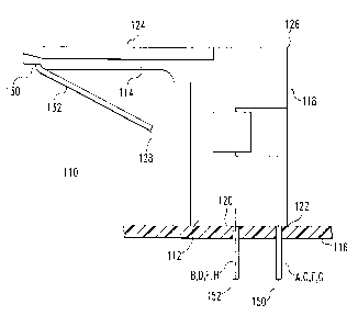
Referring to Figure lA, a side view of jack insert 110 is provided. As shown,
jack insert 110 comprises vertical support member 112 and top support member
114. Vertical
support member 112 extends vertically from printed circuit board 116 and
comprises transition
surface 118, bottom surface 120 adjacent to printed circuit board 116, and
bottom edge 122
at the intersection of the two surfaces 118 and 120. Top support member 114
extends in a
2 0 cantilevered fashion from vertical support member 112 and comprises top
surface 124 which
intersects transition surface 118 at transition edge 126. Terminals 128 extend
around leading
edge 130 of top support member 114 to provide terminal contact area 132.
Terminals 128
extend also over top surface 124 and along transition surface 118 and
ultimately terminate in
printed circuit board 116.
2 5 Figure 1 B provides a top plan view of modular jack insert 110. As shown,
top
support member 114 extends from leading edge 130 to transition edge 126. Top
support
member 114 comprises a plurality of leading edge retention members 134 for
positioning a
plurality of terminals 128 proximate to leading edge 130. In one embodiment,
eight terminals
A, B,,C, D, E, F, G, H may be positioned by leading edge retention members
134. Leading
3 o edge ~etention members 134 may comprise raised walls between which are
formed channels
CA 02298911 2000-02-17
4531 USBERG-2476 - 6 - PATENT
136 for receiving terminals 128. The walls or leading edge retention members
134 extend
from at or proximate leading edge 130 toward transition edge 126.
Proximate transition edge 126 are transition edge retention members 138 for
positioning or securing in place terminals 128. In one embodiment, transition
edge retention
members 138 extend from transition surface 118 as described in further detail
below with
reference to Figure 1 C. It should be noted, however, that transition edge
retention members
could likewise extend from top surface 124 proximate transition edge 126.
Leading edge
retention members 134 and transition edge retention members 138 provide for
positioning
terminals on top surface 124 of top support member 114. As shown in Figure 1B,
terminals
128 extend across top surface at equidistant spacing between adjacent
terminals. In other
words, terminals 128 have a constant pitch across the top surface 124. In one
embodiment this
equidistant spacing or pitch is .040 inches. Typically, the equidistant
spacing between
terminals 128 is accomplished by forming leading edge retention members 134 at
an
equidistant spacing. Transition edge retention members 138 are similarly
formed at the same
equidistant spacing. For each leading edge retention member 134, there exists
a corresponding
transition edge retention member 138 which is similarly aligned and spaced so
as to maintain
the equidistant spacing of terminals 128 across top support member 114. The
equidistant
spacing of terminals 128 across top support member 114 provides an area of
modular jack
insert 110 for application of LED's and similar devices which may be more
easily attached to
2 0 terminals with a consistent equidistant spacing.
Figure 1 C provides a plan view of transition surface 118 of vertical support
member 112. As shown, proximate transition edge 126 are formed a plurality of
transition
edge retention members 138. Transition edge retention members 138 comprise
upstanding
walls between which are formed channels 140. Terminals 128 are retained or
positioned in
2 5 channels 140. As previously noted, transition edge retention members 126
are positioned to
form channels 140 which correspond to and are aligned with channels 136 formed
by leading
. edge retention members 134. Thus, terminals 128 retained or positioned by
leading edge
retention members 134 and transition edge retention members 138 are
equidistant spaced
across top surface 124 of top support member 114.
3 0 , Bottom edge retention members 142 are formed proximate bottom edge 122.
In once embodiment, bottom edge retention members 142 comprise walls
upstanding from
CA 02298911 2000-02-17
_ '...~
4531 USBERG-2476 - 7 - PATENT
transition surface 118. Bottom edge retention members 142 extend from at or
proximate
bottom edge 122 toward transition edge retention members 138. Between bottom
edge
retention members 142 are formed channels 144 for retaining or positioning
terminals 128
proximate bottom edge 122. Bottom edge retention members 142 are positioned so
as to form
channels 144 which are equidistant spaced from each other. The spacing,
however, is typically
different from the first equidistant spacing between channels 140 provided by
transition edge
retention members 138. The second equidistant spacing, or pitch at bottom edge
122 is
typically larger than the first equidistant spacing at transition edge 126. In
one embodiment
the equidistant spacing between channels 144 formed by bottom edge retention
members 142
is .050 inches. As shown, channels 144 are offset from channels 140 formed by
transition edge
retention members 138.
On transition surface 118 between transition edge retention members 138 and
bottom edge retention members 142 is formed transition area 146. In transition
area .146
terminals 128 are transitioned from the first equidistant spacing that exists
across top surface
124 of top support member 114, to the second equidistant spacing between
terminals 128 that
exists at bottom edge 122.
It should be noted that in one embodiment, terminals 128 have barbs 148
formed therein. Barbs 148 are formed to come into contact with bottom
retention members
142 when the terminal is inserted into bottom edge retention member 142.
Specifically, barbs
2 0 148 have an interference fit with the walls of bottom edge retention
member 142 so as to
secure terminals 128 in place.
- As previously noted, modular jack insert 110 shown in Figures 1 A through 1
F
is employed in through-mounted modular jack embodiments. Accordingly,
referring to Figure
1 A proximate bottom surface 120 alternating terminals B, D, F, and H in the
plurality of
2 5 terminals transition from a first plane adjacent to transition surface 118
to a second plan that
is parallel to the first plane but which is offset into vertical support
member 112 from transition
surface 118. Thus, solder tails of terminals A, C, E, and G extend into
printed circuit board
116 at a first plane 1 SO adjacent to transition surface 118 while solder
tails of terminals B, D,
F, and H extend into printed circuit board 116 at a second plane 152 offset
from transition
3 0 surface 118.
CA 02298911 2000-02-17
~~...r. ,~:.J
4531 US/BERG-2476 - 8 - PATENT
Figures 1 D through 1 F illustrate the offset area of modular jack insert 110.
In
Figure 1 D is shown a cross section of modular jack insert taken at line A-A
of Figure 1 C. As
shown, proximate bottom edge 122 offset channel 156 extends from transition
surface 118 into
vertical support member 112. Offset channel 156 forms a recess in bottom
surface 120. The
walls of offset channel 156 are formed by the body of vertical support member
112. Figure
lE provides a detailed view of offset channel 156. In one embodiment, offset
channel is
formed at about 90 degrees relative to transition surface 118. As shown,
terminal 128
representative of terminals B, D, F, and H, extends along transition surface
118 and bends
away from transition surface 118 into offset channel 156. Thereafter, terminal
128 bends
about 90 degrees and extends out of bottom surface 120. Generally, terminals
B, D, F, and H
extends from bottom surface 120 parallel to terminals A, C, E, G but offset by
about .100
inches.
Figure 1F shows a cross section of modular jack insert 110 taken at line B-B
of Figure 1B. Line B-B designates an area of modular jack insert where the
terminal is not
free to be offset from transition surface 118. As shown, vertical support
member 112 is solid
through bottom surface 120 as indicated by cross hatching. Thus, terminals A,
C, E, and G
extend from bottom edge 122 at transition surface 118.
It should be noted that in one embodiment of the present invention, terminals
128 are lead frame as opposed to round diameter wire. Because terminals 128
are generally
2 0 applied to the exterior of insert 110 and are not routed through the body
of insert 110,
terminals 128 can comprise lead frame which is readily applied to the exterior
of terminal 110.
Figures 2A through 2D illustrate a modular jack insert in accordance with the
present invention wherein terminals 128 are surface mounted to the printed
circuit board 116.
As shown, terminals 128 extend across top surface 124 in a parallel fashion at
a constant
2 5 spacing or pitch across the entire surface 124. After traversing
transition surface 118, wherein
a transition pitch occurs as described above, in the proximity of bottom edge
122 terminals
128 bend parallel to printed circuit board 116. This is in contrast to the
configuration of Figure
1 A wherein terminals 128 are mounted into printed circuit board 116.
FIGURES 3A and 3B illustrate a modular jack which is essentially identical to
3 0 the embodiment shown in FIGURES 1 A through 1 F except that there is a
light emitting or
conv~ying source such as light pipes 140 and 142 adjacent the top surface in
an outward
CA 02298911 2000-02-17
4531 USBERG-2476 - 9 - PATENT
position relative the terminals. Such light pipes may be illuminated directly
from their rear
ends or may alternatively curve downwardly and be illuminated from a lower
position. Light
Emitting Diodes (LED's) may be also be positioned in a similar position at the
front of the top
section.outwardly from the terminals.
The present invention may be employed in other specific forms without
departing from the spirit or essential attributes thereof. For example, an
insert in accordance
with the present invention may be manufactured to accommodate any number of
terminals.
Also, various different types of retention members may employed such as
channels, bumps,
or ridges. Furthermore, the transition retention members may be attached to
either top support
1 o member or vertical support member. Finally, the pitches at which the
terminals are spaced
may vary from those mention above. Accordingly, the scope of protection of the
following
claims is not limited to the presently preferred embodiment disclosed above.