Note: Descriptions are shown in the official language in which they were submitted.
CA 02298938 2005-04-12
TITLE OF THE INVENTION
Coherent Detection Sysi:em for Multicarriex Modulation
BACKGrtOUND Or' THE INVENTIOr(
The present invention relates to a coherent
demodulation system for multi.channel modulation sys~cm used
in digital radio communication system which uses
multicarrier modulation system, for instance, OFDM
(Orthogonal Frequency Division Multiplexing) as
modulation/demodulation system. In particular, the present
invention relates to such a system which can be used in an
environment in' which trarisfE:r function or attenuation
depends upon each subcarrier in multipath transmission
circuit.
In multicarrie.r modulation system, such as OI~'DM
modulation/demotlulation system, a plurality of subcarriers
havitlg orthogonal relations tv each other are used for
transmission of communication. Tn a transmit side, an
information signal is modulated through D~PSK (hiffercntial
Quadrature Phase Shift Keyirn~) tar 16 QAM (~uadrature
Amplitude Modulation) for each subcarriers. Tha modulated
output is applied to IFFT (Inverse Fast Fourier Transform)
for inverse transformation sa that block demodulation of
OFDM sa.gnal~ is obtained.
When a UQPSK system is used for modulation of
subcarrie:rs, a delay detection system may be used Lor
demodulation in a receive side. However, a delay detection
has disadvantage that the reque=;ted Eb/No ratio must be
2
CA 02298938 2000-02-17
higher by 3 dB as compared with a coherent detection system.
Therefore, a coherent detection system is preferable for
providing a high quality transmission circuit.
When a coherent detection system is used in a
demodulation circuit in a receive side, a transmit side may
use a multi-level QAM system as a modulation system. The use
of a multi-level QAM system increases transmission rate of
information.
When multi-paths are generated in a radio transmission
channel between a transmit side and a receive side, transfer
function or attenuation for propagation in the circuit
depends upon each subcarriers. Therefore, if a coherent
detection system is used, a channel transfer function or
attenuation must be estimated for estimating amplitude
information and phase information of each subcarriers which
are subject to vary in each multipath circuit. Further, in a
radio LAN (Local Area Network) which transfers information
by using a packet, a channel transfer function or
attenuation must be estimated for each packet.
A packet has in general a preamble signal at the head
of each packet for synchronization purpose. Therefore, a
coherent detection circuit may initially carry out channel
estimation by using the preamble signal. However, if it
takes long time for initial channel estimation, a throughput
in a circuit would decrease, and therefore, a high speed
3
CA 02298938 2000-02-17
initial channel estimation is desired. Thus, an accurate
channel estimation by using short preamble signal is
essential.
In a radio LAN environment, it is possible to handle
that a transmission channel is quasi-static in which a
transmission channel does not change during a period of each
packet. In such an environment, a coherent detection is
possible only by initial channel estimation.
On the other hand, when there is large variation in an
environment, a coherent detection system must carry out to
estimate channel transfer function or attenuation
continuously.
Fig. l6 shows a block diagram of a prior OFDM coherent
detection system, in which a coherent detection is carried
out for each packet by using a preamble signal. This is
shown in S.K.Wilson, E.K.Lhayata and J.M.Cioffi, "16 QAM
Modulation with Orthogonal Frequency Devision Multiplexing
in a Rayleigh-Fading Environment", Proc. of VTC'94,
pp1660-1664.
In Fig. l6, a symbol timing detection circuit 1 detects
a symbol timing of a receive signal a101. An output a102 of
the symbol timing detection circuit 1 is applied to a S/P
(serial to parallel) conversion circuit 2.
A timing signal a114 detected by the symbol timing
detection circuit 1 is applied to a control circuit 11,
4
CA 02298938 2000-02-17
which generates a signal a105 for switching a preamble part
and a data part of a receive signal, and for deciding the
duration for holding a channel estimation signal depending
upon a period of each receive packet. The signal a105 is
applied to a hold circuit 8.
A Fourier transform circuit (FFT) 3 carries out Fourier
transformation of an OFDM demodulation signal a103. That is,
a parallel input signal a103 in time-domain is converted
into a parallel signal a104 in frequency-domain. An output
a104 of the Fourier transform circuit 3 is a receive vector
signal of each subcarriers.
The signal a104 is applied to a P/S (parallel to
serial) conversion circuit 4 which converts a parallel input
signal to a serial output signal a106. The switching circuit
5 switches the serial signal a106 into a preamble signal
a107 and a data signal alll based upon the control signal
a105 supplied by the control circuit 11.
The preamble signal a107 is applied to a channel
estimation circuit 7, which further receives a reference
preamble signal a108 from a preamble signal storage circuit
6 which stores a reference preamble signal. The channel
estimation circuit 7 carries out the channel estimation for
a preamble signal of a receive vector a107 of each
subcarriers by using a reference preamble signal a108
according to the following equation (1).
5
CA 02298938 2000-02-17
rreceive/rstore (1)
where;
r is a received preamble signal a107 (complex number)
receive
rstore is a reference preamble signal a108 (complex number)
The signal a109 which shows the result of the channel
estimation is applied to the hold circuit 8 which holds the
signal a109 for a packet period according to the control
signal a105.
On the other hand, the data signal alll is applied to a
divider circuit 9 which further receives an output a110 of
the hold circuit 8. The divider circuit 9 carries out the
division (alll/a110) so that coherent detection is obtained.
The signal a112 obtained by the coherent detection is
applied to a decision circuit 10 which decides a data (0 or
1) and outputs the decided output signal a113.
As described above, a coherent detection circuit in
Fig. l6 carries out the complex division of a received
preamble signal by a reference preamble signal stored in the
storage circuit 6 for the channel estimation.
Fig. l7 shows another prior coherent detection circuit
which has a carrier filter. This is described in P. Hoeher,
"TCM on Frequency-Selective Land-Mobile Fading Channels",
Proc. of 5th Tirrenia International Workshop Digital
Communication, Tirrenia, Italy, sept. 1991.
The most portions of Fig.l7 are the same as those of
6
CA 02298938 2000-02-17
Fig.l6, except that Fig.l7 has a carrier filter 1011 at the
output of the channel estimation circuit 107.
In Fig.l7, a symbol timing detection circuit 101
detects a symbol timing in a receive signal a1101. An output
a1102 of the symbol timing detection circuit 101 is applied
to a S/P conversion circuit 102.
A timing signal a1115 provided by the symbol timing
detection circuit 101 is applied to a control circuit 1012,
which generates a control signal a1105 according to a timing
signal a1115. The control signal a1105 functions to switch a
preamble part and a data part of a receive signal, and to
hold a signal according to duration of a receive packet.
A parallel signal a1103 of an output of the S/P
conversion circuit 102 is applied to a Fourier Transform
circuit 103 which provides a receive vector signal a1104 for
each subcarriers.
A P/S conversion circuit 104 converts a receive vector
signal a1104 for each subcarriers into a serial signal
a1106. A switching circuit 105 switches the receive vector
in serial form a1106 into a preamble signal a1107 and a data
signal allll according to the control signal a1105.
The preamble signal a1107 is applied to a channel
estimation circuit 107, which further receives a reference
preamble signal from a preamble storage circuit 106. The
channel estimation circuit 107 carries out the channel
7
CA 02298938 2000-02-17
estimation for a receive vector a1107 of each subcarriers by
using a reference preamble signal a1108 from a preamble
signal storage circuit 106 according to the equation (1).
The signal a1109 obtained by the channel estimation is
applied to a carrier filter 1011.
An output signal a1114 of the carrier filter 1011 is
applied to a hold circuit 108, which further receives a
control signal a1105, and holds an input signal a1114 for
duration of data period of a receive packet.
A data signal allll is applied to a divider 109, which
further receives an output a1110 of the hold circuit 108,
and carries out the coherent detection. The signal a1112
obtained by the coherent detection is applied to a decision
circuit 1010 for decision of data (0 or 1). Thus, the
decided data a1113 is obtained.
The coherent circuit in Fig. l7 has the advantage that
the accurate channel estimation is obtained because of the
use of a carrier filter for the estimated channel transfer
function or attenuation.
A coherent detection system provides high quality of
radio communication system as compared with a delay
detection system. Further, the use of a coherent detection
system allows the use of multi-level QAM modulation signal,
thus, higher rate communication system is obtained.
However, a prior art in Figs.l6 and 17 which carry out
8
CA 02298938 2000-02-17
the channel estimation using stored preamble signal has the
disadvantage that the channel estimation would be degraded
and no accurate coherent detection would be obtained in high
thermal noise environment.
Further, the use of a carrier filter in Fig.l7 has the
disadvantage that the size of a whole circuit of a coherent
detection system is large, and the cost of the system is
high.
SUMMARY OF THE INVENTION
It is an object, therefore, of the present invention to
overcome the disadvantages and limitations of a prior
coherent detection system by providing a new and improved
coherent detection system for multicarrier modulation.
It is also an object of the present invention to
provide a coherent detection system for multicarrier
modulation, which can provide accurate channel estimation
error under severe environment such as high thermal noise
and/or deep multi-path fading.
It is also an object of the present invention to
provide such a coherent detection system which is simple in
structure and small in circuit size.
The basic idea of the present invention resides in that
a channel estimation for a preamble signal is first carried
out as is the case of a prior art. The channel estimation
thus obtained is a provisional channel estimation in the
9
CA 02298938 2000-02-17
present invention. The accuracy of the channel estimation is
improved by processing each subcarriers in the provisional
channel estimation by using an adaptive filter. The tap
coefficients of the adaptive filter are controlled according
to a characteristic value of each subcarrier in the
provisional channel estimation.
The above and other objects are attained by a coherent
detection system for multicarrier modulation system
comprising; a Fourier transform circuit for receiving
multicarrier modulation signal modulated with a plurality of
subcarriers, and providing multicarrier demodulation so that
receive vector signal of each subcarriers is obtained; a
provisional channel estimation means which divides said
receive vector signal of each subcarriers of an output of
said Fourier transform circuit, by a reference transmit
vector signal or a transmit vector obtained by demodulation
of a receive signal, so that transfer function or
attenuation of each subcarriers on propagation is estimated;
a filter means for smoothing estimated channel transfer
function from said channel estimation means among
subcarriers; a divider means for dividing said receive
vector signal by estimated channel transfer function or
attenuation from said filter means so that said receive
vector signal is coherent detected; wherein said filter
means is an adaptive filter constituted by a transversal
CA 02298938 2000-02-17
filter in which at least one of a number of taps and tap
coefficient of each taps is adaptively controllable; a
characteristic extraction circuit receiving estimated
channel attenuation of each subcarriers obtained by said
channel estimation means is provided; a selection circuit
for selecting at least one of a number of taps and tap
coefficient of each taps of said adaptive filter according
to an output of said characteristic extraction circuit is
provided; and said selection circuit selects one of outputs
of said adaptive filter for each subcarriers according to an
output of said characteristic extraction circuit so that
estimated channel attenuation for each subcarriers is
provided.
The channel estimation by said channel estimation means
is a provisional channel estimation, which is subject to
improve by using an adaptive filter. Said divider means
provides coherent detection by dividing a receive vector by
an improved channel estimation of each subcarrier.
It should be noted that a receive signal which is
received through a multipath transmission channel having
deep fading is subject to amplitude variation for each
receive vector of a subcarrier. Further, thermal noise is
superimposed to a receive signal. The present invention
removes the affection of noise and fading by using an
adaptive filter.
11
CA 02298938 2000-02-17
However, if a filter having fixed tap coefficients is
used for all the estimated subcarriers, no accurate
estimation is possible when amplitude variation due to
fading is large. Therefore, the present invention controls
tap coefficients of an adaptive filter according to a
characteristic value of a subcarrier in order to suppress
the degradation of channel estimation by fading.
The present invention uses a plurality of filters each
having different tap coefficient from one another for
smoothing estimated channel attenuation between subcarriers,
therefore, excellent channel estimation is obtained by
selecting one of the filter outputs adaptively. In an
embodiment, a selection means selects an output of an
adaptive filter according to an output signal of a
characteristic extraction means for each subcarriers, and
therefore, difference of amplitude and/or phase rotation
among subcarriers provides less affection o channel
estimation.
A plurality of tap coefficients of an adaptive filter
are implemented merely by bit shift operation in any
embodiment. Assuming that tap coefficient of a center tap is
1, and a tap coefficient of another tap is a power of (1/2),
a product multiplied by a tap coefficient is obtained merely
by bit shift of a signal according to a tap position.
Therefore, a plurality of filter means are obtained with no
12
CA 02298938 2000-02-17
additional multiplier, and size of a circuit may be small.
A characteristic value of said characteristic
extraction means is, for instance, estimated amplitude of a
subcarrier, estimated phase rotation between adjacent
subcarriers, product of estimated amplitude and estimated
phase rotation between adjacent subcarriers, vector
difference between adjacent subcarriers, and product of
estimated amplitude and vector difference.
The larger a characteristic value is, the larger the
tap coefficient of an adaptive filter is.
Preferably, a symbol timing detection means is provided
for receiving multicarrier modulation signal modulated on a
plurality of subcarriers, and detecting a symbol timing in
the received signal. Said Fourier Transform is carried out
for the signal with a symbol timing detected.
Preferably, a phase compensation means is provided
between said channel estimation means and said adaptive
filter means, so that constant phase rotation between
adjacent subcarriers is preliminary compensated, and
compensated channel attenuation is applied to the adaptive
filter.
Preferably, a phase-compensated extrapolation means and
a phase compensation are provided between said channel
estimation means and said adaptive filter means, so that
said extrapolation means receives said estimated channel
13
CA 02298938 2000-02-17
attenuation of subcarriers at extreme ends in pass band,
effects phase compensation to a received signal according to
constant phase error between subcarriers due to an error of
an OFDM symbol detection window in said symbol timing
detection means, and extrapolates phase compensated signal,
when signals out of the pass band is requested in said
adaptive filter for processing a subcarrier close to end of
the pass band, and said phase compensation means receives
estimated channel attenuation within the pass band and
extrapolated signals out of the pass band provided by said
phase-compensated extrapolation means, effects compensation
of constant phase rotation in received signals, and applies
phase compensated signals to said adaptive filter means.
Preferably, a characteristic value compensation means
(1217) is provided between said channel estimation means
(208) and said characteristic extraction means (A), so that
said characteristic value compensation means (1217) receives
an output of said channel estimation means (208) including
constant phase error due to OFDM symbol detection window
error in said symbol timing detection means, compensating
said constant phase error and applying phase compensated
signal to said characteristic extraction means (A).
Preferably, an extrapolation means is provided between
said channel estimation means and said adaptive filter, so
that said extrapolation means receives said estimated
14
CA 02298938 2000-02-17
channel attenuation of subcarriers, and extrapolates said
estimated channel attenuation of subcarriers at extreme ends
in pass band, when signals out of the pass band is requested
in said adaptive filter for processing a subcarrier close to
end of the pass band.
Preferably, said adaptive filter means is controlled by
a measured signal of modulation system of each subcarrier.
Preferably, said adaptive filter means is a transversal
filter which controls bandwidth of the filter by a number of
taps and tap coefficient of each taps of the filter.
BRIEF DESCRIPTION OF THE DRAWINGS
The foregoing and other objects, features, and
attendant advantages of the invention will be appreciated as
the same become better understood by means of the following
description and drawings wherein;
Fig.l is shows a curve of amplitude of subcarriers in
an estimated signal,
Fig.2 is a block diagram of a transversal filter used
in the present invention,
Fig.3 shows a curve of phase rotation in a channel
estimated signal,
Fig.4 shows a curve of quantized phase rotation in a
channel estimated signal,
Fig.5 is a block diagram of an OFDM coherent detection
system according to the present invention,
CA 02298938 2000-02-17
Fig.6 shows a format of a packet signal,
Fig.7 is a block diagram of another embodiment of an
OFDM coherent detection system according to the present
invention,
Fig.8 is a block diagram of still another embodiment of
an OFDM coherent detection system according to the present
invention,
Fig.9 is a block diagram of still another embodiment of
an OFDM coherent detection system according to the present
invention,
Fig.lO shows curves indicating simulation result
showing effect of the present invention,
Fig.ll is an explanatory figure of vector difference,
Fig. l2 is a block diagram of still another embodiment
of an OFDM coherent detection system according to the
present invention,
Fig. l3 is a block diagram of still another embodiment
of an OFDM coherent detection system according to the
present invention,
Fig. l4 is a block diagram of still another embodiment
of an OFDM coherent detection system according to the
present invention,
Fig.l5 shows a format of a packet signal used in the
embodiment in Fig. l4,
Fig. l6 is a block diagram of a prior coherent detection
16
CA 02298938 2000-02-17
system, and
Fig. l7 is a block diagram of another prior coherent
detection system.
DESCRIPTION OF THE PREFERRED EMBODIMENTS
(First embodiment)
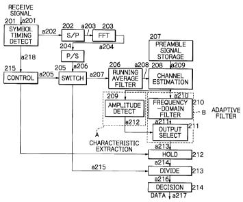
Fig.5 shows a block diagram of an OFDM coherent
detection system according to the present invention.
It is assumed that an OFDM coherent detection system in
Fig.5 is mounted in a reception system of a communication
system which handles a signal format as shown in Fig.6. In
Fig.6, a pair of preamble signals for synchronization
purpose are provided at the head of a data in each packet.
In Fig.6, GI shows guard interval, and Tw is FFT window
period.
A receive signal a201 having the signal format as shown
in Fig.6 is applied to an input of an OFDM coherent
detection system in Fig.5.
A coherent detection system in Fig.5 comprises a symbol
timing detection circuit 201, an S/P (serial to parallel)
conversion circuit 202, an FFT (Fast Fourier Transform)
circuit 203, a P/S (parallel to serial) conversion circuit
204, a switching circuit 205, a running average filter 206
of two symbols, a preamble signal storage circuit 207, a
channel estimation circuit 208, an amplitude detection
circuit 209, a frequency-domain filter 210, an output
17
CA 02298938 2000-02-17
selection circuit 211, a hold circuit 212, a division
circuit 213, a decision circuit 214, and a control circuit
215. In the embodiment of Fig. S, a characteristic extraction
circuit A of each subcarrier is comprised of an amplitude
detection circuit 209, and an adaptive filter B is comprised
of a frequency-domain filter 210 and an output selection
circuit 211.
The symbol timing detection circuit 201 detects symbol
timing in a receive signal a201. A receive signal a202 which
passes the symbol timing detection circuit 201 is applied to
the S/P conversion circuit 202 which converts a signal from
serial form into parallel form a203.
The signal a203 in parallel form is applied to the FFT
circuit 203, which carries out OFDM demodulation, in other
words, a parallel signal in time domain is transformed into
a parallel signal in frequency domain. An output signal a204
of the FFT circuit 203 is a complex signal indicating a
receive vector of each subcarrier. A parallel output signal
a204 of the FFT circuit 203 is applied to the P/S conversion
circuit 204 which converts the signal from parallel form
into serial form a206. The serial signal a206 is applied to
a switching circuit 205.
The signal a218 indicating a symbol timing detected by
the symbol timing detection circuit 201 is applied to the
control circuit 215, which generates a control signal a205
18
CA 02298938 2000-02-17
according to an input signal a218. The control signal a205
is used for switching a signal in the switching circuit 205,
and for holding a signal in the hold circuit 212 according
to the packet period of a receive packet.
The switching circuit 205 switches an input signal a206
based upon whether a signal is a preamble part a207 or a
data part a215. The preamble part a207 is applied to the two
symbols running average filter 206, which provides average
of two OFDM symbols in time-domain.
The channel estimation circuit 208 receives an average
signal a208 of the running average filter 206, and a
reference signal a209 of the preamble signal storage circuit
207. The preamble signal storage circuit 207 provides a
reference preamble signal a209 which is stored in the
storage circuit 207.
The channel estimation circuit 208 carries out the
channel estimation according to two input signals a208 and
a209, that is to say, the signal a208 which includes a
receive vector of each of a plurality of subcarriers in the
receive OFDM signal is divided by a reference signal a209
which is a known a transmit vector of said receive vector.
Thus, a transfer function or attenuation in radio
propagation path is estimated for each channels
(frequencies) of the subcarriers.
The channel estimation circuit 208 provides an output
19
CA 02298938 2004-09-17
signal a210 which has the estimated result. That output
signal a210 is applied to the amplitude detection circuit
209 in the characteristic extraction circuit A, and the
frequency-domain filter 210 in the adaptive filter B. The
amplitude detection circuit 209 provides an output signal
a212 according to amplitude of each subcarries of the input
signal a210.
The frequency-domain filter 210 is a transversal filter
as shown in Fig.2, in which a plurality of delay elements 51
(51a through 51g) which provides seven tap outputs ea~~h
having different timing, and three adders 52, 53 and 54 are
provided. A bit shift circuit between a delay element and an
adder shifts a word of a tap output by one bit or a
plurality of bits so that the most significant bit and/or
some of the adjacent bits is replaced by zero.
The frequency-domain filter 210 in Fig.2 constitutes
essentially three transversal filters having differeni~,tap
coefficients, and providing outputs SG3, SG5 and SG7. It is
assumed that the tap coefficient of the center delay element
51d is 1, and the tap coefficient of another delay element
is determined to be a power of (1/2) of the tap coeffp~cient
of the adjacent delay element.
An adder 52 provides a filter output SG3 which i;~ the
sum of third tap output 51c, fourth tap output 51d and fifth
tap output 51e. It should be noted that each tap outputs
CA 02298938 2004-09-17
applied to the adder 52 are shifted by one bit with each
other. The multiplication of tap coefficients is carr~~~ed out
by the bit shift, and therefore, no specific multiplier is
necessary for the multiplication of tap coefficients.
Similarly, an adder 53 provides a filter output SG5
which is sum of five tap outputs 51b, 51c, 51d, 51e and 51f.
An adder 54 provides a filter output SG7 which is the sum of
seven tap outputs 51a 51b, 51c, 51d, 51e, 51f, and 51c~.
A frequency-domain filter 210 in Fig.2 has the
advantage that the structure is simple as it has no
multiplier.
The signal x210 applied to the frequency-domain :filter
210 is complex signal. The filter 210 carries out the filter
operation for real part and imaginary part of complex
signal, and then, carries out the vector combination.
The output selection circuit 211 selects one of 'the
output signals a211 (one of SG3, SG5 and SG7) of the frequency-domain
filter 210, according to the amplitude 212
of each subcarrier. Said amplitude 212 is detected by the
amplitude detection circuit 209. The selected signal x213 is
applied to the hold circuit 212.
The hold circuit 212 holds the signal a213 for the
packet receive period according to the control signal a215
of the control circuit 215. The signal a214,is an output
signal of the hold circuit 212.
21
CA 02298938 2000-02-17
The division circuit 213 divides a data signal a215
included in a receive signal by the signal a214 from the
hold circuit 212. Thus, a coherent detection is carried out.
The signal a216 which is the coherent detection signal is
applied to the decision circuit 214 which decides a symbol
(1 or 0), and the decided result is output as a data a217.
A receive signal (estimated signal) which is
amplitude-deformed by multi-path fading is for instance as
shown in Fig.l, in which horizontal axis shows frequency or
subcarriers, and vertical axis shows signal amplitude of
each subcarriers. In Fig. l, it is assumed that the average
power of a receive signal is 1. A receive signal which is
received through transmission path which is subject to
fading is subject to amplitude variation for a receive
vector of each subcarriers, as shown in Fig. 1. Further,
thermal noise is superposed on a receive signal in a
receiver.
An OFDM coherent detection system in Fig.5 has a
frequency-domain filter 210 for removing affection of noise
such as thermal noise. It should be noted that if all the
subcarriers are processed by using a filter having the
common tap coefficients for all the subcarriers, accurate
estimation of transfer function of each channel is
impossible when amplitude variation of each subcarriers is
large as shown in Fig. 1.
22
CA 02298938 2000-02-17
In order to solve that problem, according to the
present coherent detection system, the output selection
circuit 211 selects on of the oututs (SG1, SG2 or SG3) of
the filter 210, according to the amplitude of each
subcarrier detected by the amplitude detection circuit 209.
Thus, a tap coefficient of the frequency-domain filter is
essentially controlled adaptively according to the amplitude
of each subcarrier.
In Fig.5, the amplitude detection circuit 209 provides
an output signal a212 which carries a quantized output dam
p
according to the amplitude (A) of the subcarriers a210, as
shown in the equation (2).
damp = 3 (1.0 <_ (A)
damp = 2 (0.5 <_ (A) < 1.0 (2)
damp = 1 (0 <_ (A) < 0.5
When the frequency-domain filter 210 provides three
outputs SGl, SG2 and SG3 as shown in Fig2, the quantized
outputs damp correspond to outputs of the filter 210.
Thus, the output selection circuit 211 selects the
output SG7 when the amplitude of a subcarrier is equal to or
higher than 1.0, the output SG5 when the amplitude of a
subcarrier is less than 1:0 and equal to or higher than 0.5,
or SG3 when the amplitude of a subcarrier is less than 0.5,
according to the output a212 of the amplitude detection
circuit 209.
23
CA 02298938 2000-02-17
Of course, the structure of a frequency-domain filter
210, the operation of quantization in an amplitude detection
circuit 209, and selection condition in an output selection
circuit 211 may be modified within the spirit of the
invention.
Thus, the bandwidth of an adaptive filter B is narrow
when the characteristic value or an amplitude of a
subcarrier is large, and is wide when the characteristic
value or an amplitude of a subcarrier is small.
Thus, a filter coefficient of a frequency-domain filter
210 is adaptively modified for each subcarriers according to
the amplitude of the subcarrier signal a210. Therefore, even
when amplitude variation among subcarriers is large as shown
in Fig.l, the accurate estimation of transfer function or
attenuation of each channel is possible.
(Second embodiment)
Fig.7 shows a block diagram of another embodiment of an
OFDM coherent detection system according to the present
invention. The same numerals in Fig.7 as those in Fig.5 show
the same members. It is assumed that the coherent detectin
system in Fig.7 processes a signal having the format as
shown in Fig.6.
The same numerals in Fig.7 as those in Fig.5 show the
same members as those in Fig.5.
24
CA 02298938 2000-02-17
An OFDM coherent detection system in Fig.7 comprises a
symbol timing detection circuit 201, an S/P (serial to
parallel) conversion circuit 202, a FFT (Fast Fourier
Transform) circuit 203, a P/S (parallel to serial)
conversion circuit 204, a switching circuit 205, a running
average circuit 206 for a pair of symbols, a preamble symbol
storage circuit 207, a channel estimation circuit 208, a
phase rotation detection circuit 309, a frequency-domain
filter 210, an output selection circuit 311, a hold circuit
212, a division circuit 213, a decision circuit 214 and a
control circuit 215. The phase rotation detection circuit
309 constitutes a characteristic extraction circuit A of
each subcarrier. The frequency-domain filter 210 and the
output selection circuit 311 constitute an adaptive filter
B.
In Fig.7, the channel estimation circuit 208 carries
out channel estimation based upon two input signals a208 and
a209. That is to say, the signal a208 which is a preamble
signal in a receive vector of each of a plurality of
subcarriers included in a receive OFDM signal is divided by
a signal a209 which is reference transmit vector. Thus, a
transfer function or an attenuation on propagation path is
estimated for each subcarriers.
A signal a210 which indicates the result of the channel
estimation in the channel estimation circuit 208 is applied
CA 02298938 2000-02-17
to the phase rotation detection circuit 309 and the
frequency-domain filter 210. In the signal a210 applied to
the phase rotation detection circuit 309, a plurality of
signal components of a plurality of subcarriers are
positioned sequentially.
The phase rotation detection circuit 309 provides a
quantized phase rotation a312 between a signal component of
a previous subcarrier and a signal component of a current
subcarrier. The output selection circuit 311 selects one of
the outputs SG3, SG5 and SG7 of the frequency-domain filter
210 according to the output signal a312 of the phase
rotation detection circuit 309, and provides selected signal
a313.
A receive signal (estimated signal) which is subject to
multi-path fading has for instance phase distribution as
shown in Fig.3, in which horizontal axis shows a subcarrier
number, and vertical axis shows phase of a signal. It should
be noted in Fig.3 that phase of a signal which is
transmitted through a propagation path having fading depends
upon a receive vector of each subcarrier. Further, phase is
affected by thermal noise in a receiver.
The OFDM coherent detection circuit in Fig.7 has a
frequency-domain filter 210 for removing affection by
thermal noise. If the frequency-domain filter had the common
tap coefficient for all the subcarriers, the transfer
26
CA 02298938 2000-02-17
function or attenuation of each channel would not be
estimated correctly, therefore, the output selection circuit
311 selects one of the outputs of the frequency-domain
filter 210 according to the phase rotation measured by the
phase rotation detection circuit 309. Thus, a tap
coefficient of the frequency-domain filter 210 is adaptively
controlled according to phase rotation of a signal.
The phase rotation detection circuit 309 in Fig.7
provides an output signal a312 of the phase rotation A
between two adjacent subcarriers, by quantizing said phase
rotation as follows.
dphase 3 (8 < pi/16)
dphase 2 (pi/16 <= a < pi/8)
(3)
dphase 1 (pi/8 <= 8)
When the signal in Fig.3 is quantized according to the
equation (3), the result as shown in Fig.4 is obtained. In
Fig.4, horizontal axis shows a subcarrier number, and
vertical axis shows quantized phase rotation dphase'
When the frequency-domain filter 210 in Fig.7 has three
outputs SG3, SG5 and SG7 as shown in Fig.2, the output
selection circuit 311 selects one of the outputs SG3, SG5
and SG7 according to values 1, 2 and 3 of the quantized
phase rotation dphase ~ respectively.
In other words, the output selection circuit 311
27
CA 02298938 2000-02-17
selects a filter output SG7 when (8 < pi/16) is satisfied, a
filter output SG5 when (pi/16 =< 8 < pi/8) is satisfied, or
SG3 when (pi/8 <= 8) is satisfied, according to an output
signal a312. Of course, it should be appreciated that any
modification of a frequency-domain filter 210 and a phase
rotation detection circuit 311 is possible to those skilled
in the art when it is requested. In any modification, a tap
coefficient of a frequency-domain filter 210 which has an
output selection circuit 311 provide an output signal a313
is adaptively controlled for each subcarriers according to
the phase rotation of the singal a210.
Therefore, it should be appreciated that the circuit in
Fig.7 can estimate transfer function or attenuation of each
channel, even when variation of phase rotation between each
channels is large.
(Third embodiment)
Fig.8 shows a block diagram of still another embodiment
of the present OFDM coherent detection system. The same
numerals as those in Fig.S show the same members. It is
assumed that the system in Fig.8 processes a signal shown in
Fig.6.
The OFDM coherent detection system in Fig.8 comprises a
symbol timing detection circuit 201, an S/P (serial to
parallel) conversion circuit 202, a FFT (Fast Fourier
28
CA 02298938 2000-02-17
transform) circuit 203, a P/S (parallel to serial)
conversion circuit 204, a switching circuit 205, a running
average filter 206 for two symbols, a preamble signal
storage circuit 207, a channel estimation circuit 208, an
amplitude detection circuit 409, a phase rotation detection
circuit 416, a multiplier 417 of two detected values, a
frequency-domain filter 210, an output select circuit 411, a
hold circuit 212, a division circuit 213, a decision circuit
214 and a control circuit 215.
The amplitude detection circuit 409, the phase rotation
detection circuit 416 and the multiplier 417 constitute a
characteristic extraction circuit A. The frequency-domain
filter 210 and the output selection circuit 411 constitute
an adaptive filter B.
In Fig.8, the channel estimation circuit 208 carries
out channel estimate according to two input signals a208 and
a209. The signal a208 which is a preamble signal included in
a receive vector of a subcarrier in a receive OFDM signal is
divided by the signal a209 which is a reference transmit
signal. Thus, transfer function in propagation path is
estimated for each channel of each subcarriers.
The signal a210 which carries the estimated result in
the channel estimation circuit 208 is applied to the
amplitude detection circuit 409, the phase rotation
detection circuit 416 and the frequency-domain filter 210.
29
CA 02298938 2000-02-17
The signal a210 has a plurality of signal components of
subcarriers sequentially.
The amplitude detection circuit 409 provides an output
signal a412 which carries quantized amplitude of each
subcarriers in the signal a210, as is the case of the
amplitude detection circuit 209 in Fig. S.
The phase rotation detection circuit 416 provides an
output signal a418 which carries quantized phase rotation
between a previous subcarrier and a current subcarrier for
each subcarriers in an input signal a210. The multiplier
circuit 417 provides the product of the signals a412 and
a418 so that the charactristic signal a419 of each
subcarrier is provided. The signal a419 is a quantized value
,such as 1, 2 or 3, which is applied to the output selection
circuit 411.
The output selection circuit 411 selects one of the
outputs (SG3, SG5 and SG7 in Fig.2) of the frequency-domain
filter 210, according to the output signal a419 of the
multiplier circuit 417. The selected signal is output as
a413.
The OFDM coherent detection system in Fig.8 measures
both the amplitude of the signal a210, and the phase
rotation of the signal a210, as the characteristic value of
each subcarrier, so that the characteristic of the
frequency-domain filter 210 which processes a receive signal
CA 02298938 2000-02-17
is determined.
Thus, it should be appreciated that the coherent
detection system in Fig.8 can estimate transfer function or
attenuation of each channel even when variation of amplitude
and phase rotation of each channel is large as shown in
Figs.l and 3.
(Fouth embodiment)
Fig.9 shows a block diagram of still another embodiment
of the present OFDM coherent detection system. The same
members as those in Fig.8 show the same members. It is
assumed that the OFDM coherent detection system in Fig.9
processes a signal having the format shown in Fig.6.
The OFDM coherent detection system in Fig.9 comprises a
symbol timing detection circuit 201, an S/P (serial to
parallel) conversion circuit 202, an FFT (Fast Fourier
Transform) circuit 203, a P/S (parallel to serial)
conversion circuit 204, a switching circuit 205, a running
average filter 206 for two symbols, a preamble signal
storage circuit 207, a channel estimation circuit 208, a
vector difference detection circuit 509, a frequency-domain
filter 210, an output selection circuit 511, a hold circuit
212, a division circuit 213, a decision circuit 214 and a
control circuit 215.
The vector difference detection circuit 509 constitutes
31
CA 02298938 2000-02-17
a characteristic extraction circuit A. The frequency-domain
filter 210 and the output selection circuit 511 constitute
an adaptive filter B.
In Fig.9, the channel estimation circuit 208 carries
out channel estimation based upon two input signals a208 and
a209. In other words, the signal a208 which carries a
preamble signal in a receive vector of a subcarrier in a
receive OFDM signal is divided by a signal a209, which is
provided by the preamble signal storage circuit 207 as a
reference transmit vector. Thus, transfer function or
attenuation in propagation path is estimated for each
channel of a subcarrier.
The signal a210 which is an output of the estimation
circuit 208 is applied to the vector difference detection
circuit 509 and the frequency-domain filter 210. The signal
a210 carries a plurality of signal components of subcarriers
sequentially.
The OFDM coherent detection system in Fig.9 has the
vector difference detection circuit 509, instead of the
amplitude detection circuit 409 and the phase rotation
detection circuit 416 in Fig.8.
The vector difference detection circuit 509 detects the
absolute value of the vector difference of the input signal
a210, without separating amplitude and phase from the
vector. The vector difference detection circuit 509 provides
32
CA 02298938 2000-02-17
an output signal a512 which carries a quantized value of the
vector difference of signal components between a previous
subcarrier and a current subcarrier. Therefore, the signal
a512 is the vector difference between adjacent two
subcarriers.
The output selection circuit 511 selects one of the
outputs SG3, SG5 and SG7 of the frequency-domain filter 210,
as shown in Fig.2. The selected signal is the output signal
a513.
Therefore, the OFDM coherent detection circuit in Fig.9
determines the characteristic of the frequency-domain filter
210 according to the vector difference between subcarriers
in the signal a210.
Therefore, the accurate estimation of each channel
transfer function or attenuation is carried out, even when
the variations of both the amplitude and the phase rotation
between channels are large as shown in Figs.l and 3.
In order to confirm the effect of the present OFDM
coherent detection system, a computer simulation has been
carried out. The simulation assumes the following
conditions, and calculates packet error rate of the system
in Fig.8 (present invention), and Fig. l6 (prior art).
Format of receive signal; same as Fig.6
Modulation system of subcarrier; 16 QAM
33
CA 02298938 2000-02-17
Error correction; convolutional coding with coding
ratio 1/2, and decoding by Vitabi algorithm
Symbol timing detection; ideal
Transmit packet length; 64 bytes
Transmission path assumes Rayleigh fading environment
(delay spread (r.m.s.)=150 nS) of 30 waves with O.B.O
(Output Back Off)=5 dB, considering non-linearity of a
transmit amplifier.
Fig.lO shows the result of the simulation. In Fig.lO,
the horizontal axis shows Eb/No (dB) (ratio of signal energy
for each bit and one-sided spectral density of additive
white Gaussian noise), and the vertical axis shows packet
error rate (PER).
It should be noted in Fig.lO that the present invention
has improved Eb/No by 0.5 dB when PER=0.1. Therefore, the
present invention provides accurate channel estimation,
suppresses degradation of PER, and improves the total
performance .
(Fifth embodiment)
A subcarrier No.32 in Fig.l has high amplitude and
large difference from that of an adjacent subcarrier. When
an amplitude is high and difference from that of an adjacent
subcarrier is large, if a tap coefficient of a filter is
34
CA 02298938 2000-02-17
determined only depending upon amplitude, the filter would
have large tap coefficient, and would not follow the
frequency-domain change. Therefore, a tap coefficient must
further be controlled by a characteristic value which
indicates variation from an adjacent subcarrier.
Therefore, according to the present embodiment, an
adaptive filter is controlled according to not only an
amplitude of a subcarrier but also a vector difference
between two adjacent subcarriers.
Fig.ll shows an explanation of a vector difference. In
Fig.ll, a signal plane is defined of each subcarrier in
direction of frequency, and a receive signal vector (an
estimated signal vector) is shown on the signal plane. It is
assumed for simplicity that all the carriers have the signal
point (Ich, Qch)=(0, 1), and suffer from only amplitude
variation.
In Fig.ll, a vector difference between a subcarrier #A
and a subcarrier #A+1 close to the point A, and a vector
difference between a subcarrier #B and a subcarrier #B+1
close to the point B appear the same. Therefore, the present
embodiment takes not only vector difference but also
amplitude of a subcarrier by weighting them, so that a
filter can follow the change in frequency domain even when
variation of channel transfer function or attenuation in
frequency domain is large and delay spread is large, and
CA 02298938 2000-02-17
degradation of channel estimation by noise is suppressed.
Fig. l2 shows a block diagram of the current embodiment,
which assumes to process a signal format of Fig.6, and the
same numerals as those in Fig.5 show the same members.
The coherent detection system in Fig.l2 comprises a
running average filter 206 of two symbols, an amplitude
detection circuit 209, an vector difference detection
circuit 509 a frequency-domain filter 210, a multiplier
circuit 417 and an output selection circuit 211.
The running average filer 206 of two symbols receives
preamble signals a207, and provides running average of two
preamble signals in time axis. The amplitude detection
circuit 209 receives a channel estimation signal a210, and
provides amplitude detection signal a212 depending upon
amplitude of the estimated channel signal. The vector
difference detection circuit 509 receives the channel
estimation signal a210, and provides an output signal a512
which is vector difference between a previous subcarrier and
a current subcarrier. The multiplier circuit 417 receives
the amplitude detection signal a212 and the vector
difference detection signal a512, and provides the product
of those two signals as the characteristic value of a
receive packet. The frequency-domain filer 210 receives a
channel estimation signal a210, and provides a three-taps
output, a five-taps output and a seven-taps output as shown
36
CA 02298938 2000-02-17
in Fig.2, as filter outputs a211 (SG3, SG5, or SG7). The
output selection circuit 211 selects one of the outputs of
the filter depending upon the output signal a211b of the
multiplier 417.
A characteristic extraction circuit A is comprised of
the amplitude detection circuit 209, the vector difference
detection circuit 509, and the multiplier circuit 417. An
adaptive filter B is comprised of the frequency-domain filer
210 and the output selection circuit 211.
A receive signal a201 is applied to the symbol timing
detection circuit 201 which detects a symbol timing. An
output a202 of the symbol timing detection circuit 201 is
applied to the S/P conversion circuit 202. The converted
parallel signal a203 is applied to the FFT circuit 203 which
carries out OFDM demodulation and provides receive vector
a204 of each subcarriers. The P/S conversion circuit 204
carries out the parallel to serial conversion of a
subcarrier receive vector signal a204, and provides the
serial signal a206.
On the other hand, the timing signal a218 is applied to
the control circuit 215, which provides a control signal
a205. The control signal a205 is applied to the switching
circuit 205 which carries out the switching of a preamble
signal and a data signal of a receive signal, and a hold
circuit 212 which holds a signal during a channel estimation
37
CA 02298938 2000-02-17
signal hold time. The switching circuit 205 switches a
preamble signal a207 and a data signal a215 according to the
control signal a205. The preamble signal a207 is applied to
the running average filter 206 which provides average of two
preambles in time axis. The output a208 of the average
filter 206 is applied to the channel estimation circuit 208
which carries out the channel estimation by using the
reference preamble signal in the preamble signal storage
circuit 207.
The channel estimation signal a210 is applied to the
amplitude detection circuit 209 which measures amplitude of
the estimated channel signal a210 and provides the amplitude
detection signal a212. Further, the channel estimation
signal a210 is applied to the vector difference detection
circuit 509, which provides vector difference detection
signal a512 between a previous subcarrier and a current
subcarrier. The amplitude detection signal a212 and the
vector difference detection signal a512 are applied to the
multiplier circuit 417, which provides the characteristic
value depending upon each receive packet. The channel
estimation signal a210 is further applied to the
frequency-domain filter 210, which provides filter outputs
a211. The output selection circuit 211 selects one of the
filter outputs a211 according to the product a211b of the
output of the multiplier circuit 417 so that the larger the
38
CA 02298938 2000-02-17
product a211b is, a filter output relating to the larger tap
coefficient is selected.
The output selection signal a213 is applied to the hold
circuit 212, which holds the output selection signal a213
during the channel estimation signal hold period according
to the control signal. The output a214 of the hold circuit
212 is applied to the divider circuit 213 which also
receives a data signal a215, so that the former signal a214
is divided by the latter signal a215 to perform coherent
detection. The coherent detection signal a216 is applied to
the decision circuit 214, which provides an output data
a217.
(Sixth embodiment)
Fig. l3 is a block diagram of still another embodiment
of the present coherent detection system. It is assumed that
the system in Fig.l3 processes a signal format shown in
Fig.6, and the same numerals as those in the previous
embodiments show the same members.
The feature of this embodiment is, first, a phase
compensation circuit 1219 is provided at an input of an
adaptive filter 210 so that a constant phase rotation in a
signal is removed before a signal is applied to the adaptive
filter 210. Another feature of this embodiment is that a
phase compensated extrapolation circuit 1218 is provided at
39
CA 02298938 2000-02-17
an input of said compensation circuit 1219 so that signals
out of the pass band are phase-compensated and extrapolated
into a signal. Said signals out of the pass band are
necessary for an adaptive filter B when the adaptive filter
B processes a subcarrier close to ends of the pass band.
Still another feature of this embodiment is that a
subcarrier phase compensation circuit 1217 is provided at an
input of a characteristic extraction circuit A so that phase
rotation between adjacent subcarriers is compensated for
characteristic extraction.
Fig. l3 shows an embodiment that all of the phase
compensation circuit 1219, the phase-compensated
extrapolation circuit 1218, and the subcarrier phase
compensation circuit 1217 are provided, and those features
are added to the embodiment of Fig. l2. It should be noted
that those features may also be added to another embodiment,
for instance the embodiment of Fig.8, and further it is
possible to those skilled in the art that one or two of
three features may be added to any previous embodiment.
In Fig. l3, a receive signal a201 is applied to a symbol
timing detection circuit 201 for detecting a symbol timing.
A timing signal a202 is applied to a control circuit 215,
which provides a control signal a205. The control signal
a205 determines the timing for opening a receive OFDM
window, for switching a preamble part and a data part of a
CA 02298938 2000-02-17
receive signal, and for holding a channel estimation signal.
A receive signal a201 is further applied to a S/P (serial to
parallel) conversion circuit 202 which outputs an OFDM
symbol according to the control signal and provides an
output signal a203 in parallel form. The signal a203 is
applied to an FFT (Fast Fourier Transform) circuit 203 which
carries out OFDM demodulation and provides a receive vector
a204 of a subcarrier. A P/S (parallel to serial) conversion
circuit 204 converts the signal into serial form and
provides an output signal a206 in serial form. A switching
circuit 205 switches the signal a206 into a preamble signal
a207 and a data signal a215 according to the control signal
a205. The preamble signal a207 is applied to a running
average filter 206 which provides an average of two symbols
on time axis. An output a208 of the running average filter
206 is applied to a channel estimation circuit 208, which
further receives a reference preamble a209 from a preamble
signal storage circuit 207, and carries out channel
estimation. A channel estimation signal a210 is applied to
an amplitude detection circuit 209. Further a channel
estimation signal a210 is applied to a subcarrier phase
compensation circuit 1217 which carries out the phase
compensation according to the following equation, and
provides a phase compensation signal s221.
- -
ri _ Pi Pile
41
CA 02298938 2000-02-17
where Pi is a receive signal of each subcarrier, and a is
phase rotation between adjacent two subcarriers.
The channel estimation signal a210 is further applied
to the phase-compensated extrapolation circuit 1218, which
extrapolates a signal out of the pass band by using the most
extreme subcarriers for the filter process, and then phase
of each extrapolated signal is compensated.
The extrapolated signal s222 is applied to the phase
compensation circuit 1219 which compensates constant phase
error, and provides the phase compensated output signal s223
to the frequency-domain filter 210. The frequency-domain
filter 210 provides the smoothed filter output a211 in
frequency axis.
The amplitude detection circuit 209 detects the
amplitude of the estimated signal a210, and provides the
amplitude detection signal a212. The phase compensated
signal s221 is applied to the vector difference detection
circuit 509, which provides the vector difference output
a512 between a previous subcarrier and a current subcarrier.
The amplitude detection signal a212 and the vector
difference detection signal a512 are applied to the
multiplier 417, which provides the characteristic value of a
receive packet by the product of two inputs. The output
selection circuit 211 selects one of the filter outputs
according to the output a211b of the multiplier 417. Then,
42
CA 02298938 2000-02-17
the selected signal a213 is applied to the hold circuit 212,
which holds the selected output signal a213 for channel
estimation signal hold period according to the control
signal a205. The output a214 of the hold circuit 212 is
applied to the divider circuit 213, which also receives a
data signal a215, and provides the equalization of an input
channel transfer function, or coherent detection. The
coherent detection signal a216 is applied to the decision
circuit 214, which decides a data (1 or 0) and provides an
output data a217.
(Seventh embodiment)
Fig. l4 shows a block diagram of still another
embodiment of the present coherent detection system. The
same numerals as those in the previous embodiments show the
same members.
The feature of the embodiment in Fig.l4 is that an
adaptive filter B is controlled according to modulation
system of each subcarrier. For instance, when a number of
multiplicity n of modulation is large (when a number n of
nQAM modulation system is large), an adaptive filter is
controlled so that a bandwidth of the filter is wide.
It is assumed in the present embodiment that a preamble
signal as shown in Fig.l5 is used for channel estimation. In
Fig.l5, an information indicating modulation system of a
43
CA 02298938 2000-02-17
subcarrier is transmitted from a transmit side.
In Fig. l4, a receive signal a201 is applied to a symbol
timing detection circuit 201 which detects symbol timing.
The timing detection signal a202 is applied to a control
circuit 215, which provides a control signal. The control
signal is used for determining to open a receive OFDM
window, a timing to switch a receive signal into a preamble
part and a data part, and a period to keep a channel
estimation signal. A receive signal a201 is further applied
to a S/P (serial to parallel) conversion circuit 202 which
outputs OFDM symbol according to the control signal. The S/P
conversion signal a203 is applied to an FFT (Fast Fourier
Transform) circuit 203 for OFDM demodulation, and provides a
subcarrier receive vector signal a204. A P/S (parallel to
serial) conversion circuit 204 converts a subcarrier receive
vector signal in parallel form into serial form, and
provides the converted serial output signal a206. The
switching circuit 205 switches a receive signal into a
preamble signal a208 and the other signal a215.
The channel estimation circuit 208 carries out the
channel estimation by using a reference preamble signal a209
stored in the preamble signal storage circuit 207, and
provides channel transfer function or attenuation a210 of
each subcarrier. The channel estimation is possible not only
by using only a preamble signal, but also by first
44
CA 02298938 2000-02-17
estimation of channel transfer function or attenuation by
using a preamble signal and secondly updating the estimated
value by using a data after data decision through reverse
modulation. The channel estimation signal a210 is applied to
the frequency-domain filter 210, and an output a213 of the
frequency-domain filter 210 is applied to a hold circuit
212. The hold circuit 212 keeps an output a213 of the filter
210 for hold time of channel estimation signal according to
the control signal. The divider circuit 213 receives a
signal a215 which excludes a preamble signal and an output
signal a214 of the hold circuit 212, and carries out channel
equalization or coherent detection, and provides a coherent
detection signal a216. The switching circuit 2212 switches a
coherent detected signal into an information s2212b which
shows subcarrier modulation system and data signal s2212a.
The information s2212b of the subcarrier modulation system
is applied to a demodulation circuit 2214 of a subcarrier
modulation system to measure the modulation system of
subcarriers. The measured modulation system is an output
signal s2214, which is applied to the frequency-domain
filter 210 for selecting tap coefficients.
(Effect of the invention)
As described above in detail, according to the present
multicarrier coherent detection system, a filter output is
CA 02298938 2000-02-17
selected according to actual environment of each channel,
and therefore, an accurate channel estimation is obtained as
compared with a prior art. Therefore, an improved coherent
detection system is obtained with a little increase of size
of a circuit.
From the foregoing it will now be apparent that a new
and improved multicarrier coherent detection system has been
found. It should be appreciated of course that the
embodiments disclosed are merely illustrative and are not
intended to limit the scope of the invention. Reference
should be made to the appended claims, therefore, for
indicating the scope of the invention.
20
46