Note: Descriptions are shown in the official language in which they were submitted.
CA 02299133 2000-02-23
TITLE OF THE INVENTION
VOLTAGE-CONTROLLED OSCILLATORS WITH REDUCED INCIDENTAL
FREQUENCY MODULATION AND USE IN PHASE LOCKING OSCILLATORS
BACKGROUND OF THE INVENTION
Field of the Invention
The present invention relates generally to voltage-controlled oscillators
and their use in phase locking oscillators. More particularly, the present
invention pertains to voltage-controlled oscillators with reduced incidental
frequency modulation and their use in phase locking oscillators.
Description of the Related Art
As is well known, frequencies in electronic circuits have a tendency to
drift. Therefore, phase locking oscillators are used widely to provide
electronic
circuits that are highly immune to frequency drift. The output frequency is
phase locked to a reference frequency that is commonly crystal controlled.
In phase locking oscillators, an edge-triggered phase detector compares
a frequency that is fed back from a voltage-controlled oscillator (VCO) with a
5 reference frequency, and delivers voltage pulses that are a function of the
phase
difference between the reference frequency and the feedback frequency to an
integrator, or filter.
The integrator integrates the voltage pulses received from the phase
detector and then delivers the integrated output to the VCO, driving the VCO
10 away from its free-running frequency and toward phase lock with the
reference
oscillator. Although it may take several or many cycles, eventually the VCO
will lock onto the reference frequency, which is commonly crystal controlled.
While some phase locking oscillators are used to provide a carrier that
is not modulated, the output frequencies of phase locking oscillators may be
frequency modulated on an ac basis at any frequency that is higher than the
natural loop frequency by applying a modulating voltage to the VCO.
Alternately, the output frequency of the phase locking oscillator may be do
modulated, or both ac and do modulated, as taught by Lautzenhiser in U.S.
Patent Nos. 5,091,706, issued 25 February 1992; 5,097,230, issued 17 March
1992; and 5,311,152, issued 10 May 1994.
CA 02299133 2000-02-23
2
When a VCO is used in a high performance electronic circuit such as a
phase locking oscillator, incidental frequency modulation (IFM) of the output
frequency of the VCO is a critical problem, as will become apparent as this
discussion continues.
A basic principle of electronic and electrical design is that any wire
conductor or any trace on a circuit board that vibrates through an electrical
field will induce a voltage in that wire or trace. And, of course, it is
inherent in
electronic circuits that there are various electrical fields.
Induced voltages, or noise, or voltage spikes that are superimposed on
a voltage driving a voltage-controlled oscillator, will cause unwanted
modulation of output frequency. This unwanted modulation is called incidental
frequency modulation. Incidental frequency modulation is a serious problem in
high performance electronic circuits.
For instance, if a given voltage-controlled oscillator has a sensitivity of
20 MHz per volt, an induced voltage of only 1.0 millivolt will cause
incidental
frequency modulation of 20 kHz. Since 20 kHz is the maximum allowable
incidental frequency modulation for many military devices, vibration of a wire
conductor or trace leading to a VCO can consume the entire allowable
incidental frequency modulation bandwidth.
Of course, every attempt is made to keep wire conductors and traces
short, thereby minimizing the problem of incidental frequency modulation.
However, often an electrical connection must be made from some relatively
distant portion of a circuit board, or even from a separate board.
Voltage-controlled oscillators have many uses in addition to being a
part of a phase locking loop, and whenever voltage-controlled oscillators are
used in high performance electronic circuits, incidental frequency modulation
is
potentially a serious problem.
Reducing the sensitivity (MHz per volt) of the VCO by a factor of ten
would reduce incidental frequency modulation caused by induced voltages by
the same factor of ten. However, the maximum frequency locking range, or
capture range, that could be achieved would also be reduced by a factor of
ten,
in many applications preventing a phase locking oscillator from phase locking.
CA 02299133 2000-02-23
3
In summary, while prior art crystal-controlled phase locking oscillators
provide improved frequency stability by minimizing both short term and long
term frequency drift, voltage spikes and other electrical noise, whether
emanating from the integrator, the lead connecting the integrator to the VCO,
or from some other induced voltage, widen the required bandwidth, and make
it difficult to manufacture electronic apparatus within military
specifications.
BRIEF SUMMARY OF THE INVENTION
Voltage-controlled oscillators (VCOs) are provided in which incidental
frequency modulation (IFM) is reduced by a factor up to 10.0 or more.
Therefore, phase locking oscillators using VCOs of the present invention also
enjoy reduced incidental frequency modulation.
In all embodiments of the present invention, reduction in incidental
frequency modulation is reduced by reducing a frequency-deviation-sensitivity
of the VCO. And, in all embodiments, the VCO includes means for restoring a
maximum frequency range and a capture range of the phase locking oscillator.
In several embodiments, the frequency-deviation-sensitivity is reduced
when a frequency of a frequency-control voltage applied to a VCO is above a
predetermined roll-off frequency. And the frequency-deviation-sensitivity is
increased, or restored, when the VCO is subjected to a frequency-control
voltage whose frequency is below the predetermined roll-off frequency. In like
manner, the VCO responds at the higher frequency-deviation-sensitivity if the
frequency-control voltage is a constant do voltage.
The result is that, when used as a part of a phase locking oscillator, the
voltage-controlled oscillator responds at the reduced frequency-deviation-
sensitivity to loop frequencies which are above the predetermined roll-off
frequency, and at full frequency-deviation-sensitivity to loop frequencies,
including dc, which are below the predetermined roll-off frequency.
Therefore, voltage spikes and other electrical noise are attenuated in
direct proportion to the reduction in frequency-deviation-sensitivity of the
VCO,
and undesirable incidental frequency modulation caused by the voltage spikes
and other electrical noise is attenuated by the same ratio.
CA 02299133 2000-02-23
4
While the frequency-deviation-sensitivity of the voltage-controlled
oscillator is reduced in response to frequencies above the predetermined roll-
off
frequency, both the capture range and the frequency response of the phase
locking loop remains unaffected.
In two embodiments of the VCOs of the present invention, incidental
frequency modulation also is attenuated by reducing a frequency-deviation-
sensitivity thereof, but a maximum frequency range of the VCO is maintained
by means, included in the VCO, for augmenting a frequency-control voltage
applied thereto.
Therefore, all of the VCOs of the present invention include means for
reducing the frequency-deviation-sensitivity, whereby a maximum frequency
range is also reduced, and all of the VCOs include means for restoring the
maximum frequency range. When used in a phase locking oscillator the means
for restoring the maximum frequency range also provides means for restoring a
capture range of the phase locking oscillator that was reduced by reducing the
frequency-deviation-sensitivity of the VCOs.
All components of the VCOs, both for reducing the frequency-
deviation-sensitivity and for restoring the maximum frequency range thereof,
are
contained in a shielded can, thereby isolating all of their components from
stray
voltage fields.
By using VCOs of the present invention in phase locking oscillators,
voltage spikes, other electrical noises, ac modulation signals, and incidental
frequency modulation are attenuated. This is true for voltage spikes and other
electrical noises developed within the phase locked loop, or introduced to the
VCO from an external source.
In a first aspect of the present invention, a method for controlling an
output frequency comprises driving the output frequency away from a free
running frequency in response to a frequency-control voltage and in proportion
to both the frequency-control voltage and a frequency-deviation-sensitivity,
and
the improvement comprises: reducing the frequency-deviation-sensitivity,
whereby noise spikes, incidental frequency modulation, and a maximum
frequency range for a maximum frequency-control voltage are all reduced; and
CA 02299133 2000-02-23
restoring at least a portion of the reduced maximum frequency range
irrespective of a frequency of the frequency-control voltage.
In a second aspect of the present invention, a method for phase locking
an output frequency to a reference frequency comprises comparing a feedback
5 frequency to the reference frequency, producing a frequency-control voltage
in
response to the comparing step, driving the output frequency toward phase lock
in response to the frequency-control voltage, and the improvement comprises:
reducing a frequency-deviation-sensitivity of the output frequency to the
frequency-control voltage, whereby noise spikes, incidental frequency
modulation, and a capture range are all reduced; and restoring at least a
portion
of the reduced capture range irrespective of the reduced frequency-deviation-
sensitivity.
In a third aspect of the present invention, a method for controlling an
output frequency comprises driving the output frequency away from a free-
running frequency in response to a frequency-control voltage and in proportion
to both the frequency-control voltage and a frequency-deviation-sensitivity,
and
the improvement comprises: reducing the frequency-deviation-sensitivity,
whereby noise spikes, incidental frequency modulation, and a maximum
frequency range for a maximum frequency-control voltage are all reduced; the
reducing step comprises dividing the frequency-control voltage prior to the
driving step; restoring at least a portion of the reduced maximum frequency
range; and the restoring step comprises proportionally combining the divided
frequency-control voltage and an other voltage prior to the driving of the
output
frequency.
In a fourth aspect of the present invention, a method for phase locking
an output frequency to a reference frequency comprises comparing a feedback
frequency to the reference frequency, producing a frequency-control voltage in
response to the comparing step, driving the output frequency toward phase lock
in response to the frequency-control voltage, and the improvement comprises:
reducing a frequency-deviation-sensitivity, whereby noise spikes, incidental
frequency modulation, and a capture range are all reduced; the reducing step
comprises dividing the frequency-control voltage prior to the driving step;
restoring at least a portion of the reduced capture range; and the restoring
step
CA 02299133 2000-02-23
6
comprises proportionally combining the divided frequency-control voltage and
an other voltage prior to the driving of the output frequency.
In a fifth aspect of the present invention, a radio frequency oscillator
produces a free-running output frequency at an output frequency terminal, the
output frequency is changed at a predetermined frequency-deviation-sensitivity
in response to a frequency-control voltage applied to an input voltage
terminal,
and the improvement comprises: means for reducing the frequency-deviation
sensitivity, whereby voltage spikes, resultant incidental frequency
modulation,
and a maximum frequency range for a maximum frequency-control voltage are
reduced; and means for restoring at least half of the reduced maximum
frequency range irrespective of the reduced frequency-deviation-sensitivity.
In a sixth aspect of the present invention, a phase locking oscillator
comprises a phase detector, an integrator that produces a frequency-control
voltage, a radio frequency oscillator that produces an output frequency in
response to the frequency-control voltage, and the improvement comprises:
means for reducing a frequency-deviation-sensitivity of the radio frequency
oscillator to the frequency-control voltage, whereby voltage spikes, resultant
incidental frequency modulation, and a capture range are all reduced; and
means for restoring at least half of the reduced capture range irrespective of
a
frequency of the frequency-control voltage.
In a seventh aspect of the present invention, a radio frequency
oscillator produces a free-running output frequency at an output frequency
terminal, the output frequency is driven away from the free-running output
frequency at a predetermined frequency-deviation-sensitivity in response to a
frequency-control voltage applied to an input voltage terminal, and the
improvement comprises: means, comprising means for dividing the frequency-
control voltage, for reducing the frequency-deviation-sensitivity, whereby
voltage spikes, resultant incidental frequency modulation, and a maximum
frequency range for a maximum frequency-control voltage are reduced; means
for providing an other voltage; and means, comprising means for proportionally
combining the divided frequency-control voltage and the other voltage for
restoring at least half of the reduced frequency range.
CA 02299133 2000-02-23
7
In an eighth aspect of the present invention, a phase locking oscillator
comprises a phase detector, an integrator that produces a frequency-control
voltage, a radio frequency oscillator that produces an output frequency in
response to the frequency-control voltage, and the improvement comprises:
means, comprising means for dividing the frequency-control voltage, for
reducing a frequency-deviation-sensitivity, whereby voltage spikes, resultant
incidental frequency modulation, and a capture range are reduced; means for
providing an other voltage; and means, comprising means for proportionally
combining the divided frequency-control voltage and the other voltage, for
restoring at least half of the reduced capture range.
BRIEF DESCRIPTION OF THE SEVERAL VIEWS OF THE DRAWINGS
FIGURE 1 is a schematic of a prior art voltage-controlled oscillator
(VCO);
FIGURE 2 is a schematic of a first embodiment of a VCO of the present
invention that reduces incidental frequency modulation (IFM) without reducing
a maximum frequency range thereof;
FIGURE 3 is a schematic of an embodiment of a reduced IFM phase
locking oscillator of the present invention that utilizes the reduced IFM VCO
of
FIGURE 2, but the circuitry of FIGURE 3 would be a prior art phase locking
oscillator if used with the prior art VCO of FIGURE 1;
FIGURE 4 is a parameter space plot calculated in accordance to the
Boundary Crossing Theorem of Frazer and Duncan, showing stable
combinations of resistors as a function of VCO gain, with stable combinations
of resistors on the left sides of their respective gain curves;
FIGURE 5 is a schematic of a variation of the reduced IFM phase
locking oscillator of FIGURE 3 in which a reduced IFM VCO thereof includes
both a standard VCO and an ac voltage divider;
FIGURE 6 is a schematic of an embodiment of a reduced IFM phase
locking oscillator in which a reduced IFM VCO thereof includes a pair of
diodes that increase phase locking speed;
CA 02299133 2000-02-23
8
FIGURE 7 is a schematic of a preferred embodiment of a reduced IFM
phase locking oscillator in which a reduced IFM VCO thereof includes a pair of
transistors that increase phase locking speed;
FIGURE 8 is a schematic of an embodiment of a reduced IFM phase
locking oscillator in which a reduced IFM VCO thereof includes a PROM that
provides a channelizing voltage, and resistors that proportionally combine the
channelizing voltage with a frequency-control voltage, thereby restoring both
a
maximum frequency range of the VCO and a capture range of the phase
locking oscillator; and
FIGURE 9 is a schematic of an embodiment of a reduced IFM phase
locking oscillator in which a reduced IFM VCO thereof generates a
supplementary voltage and proportionally combines the supplementary voltage
with a frequency-control voltage applied to the VCO, thereby restoring a
maximum frequency range of the VCO and a capture range of the phase
locking oscillator.
DETAILED DESCRIPTION OF THE INVENTION
Referring to FIGURE 1, a prior art voltage-controlled oscillator (VCO),
or radio frequency oscillator, 10 includes: a transistor Q1; inductors L1 and
L2;
resistors R1, R2, and R3; coupling resistor R4; capacitors C1, C2, C3, and C4;
and a varactor, or voltage-variable capacitance diode, CR1. Typically, an
electrical ground, as shown in FIGURE 1, is connected to a shielding can 12
that is symbolically represented by a dashed line, that surrounds the VCO 10,
and that protects the VCO 10 from magnetic fields.
Values for these components and a technical explanation for this
circuitry may be found in standard text books. However, the principles of the
present invention may be practiced using any suitable VCO. As used herein,
the VCO 10 represents any suitable VCO or radio frequency oscillator.
Briefly, when a supply voltage is applied to a supply terminal VCC, the
VCO 10 provides a free-running radio frequency (RF) output frequency at an
output frequency terminal RF. And when a voltage, whether varying or
constant, is applied to an input voltage terminal VT, the output frequency at
the
terminal RF varies from the free-running frequency of the VCO 10.
CA 02299133 2000-02-23
9
The RF output frequency of the VCO 10 will change from its free-
running frequency in accordance with the sensitivity of the VCO 10 to voltages
applied to the input voltage terminal VT. This sensitivity is measured in
units
of frequency change per unit of input voltage change. That is, the sensitivity
of
the VCO 10 may be measured in megahertz per volt, and a typical value is 20
megahertz per volt.
Referring now to FIGURE 2, in a first embodiment of the present
invention, a reduced IFM voltage-controlled oscillator, or variable frequency-
deviation-sensitivity voltage-controlled oscillator, or radio frequency
oscillator
20 includes the VCO 10 of FIGURE 1. In addition, the VCO 20 includes a
resistor R5 and a capacitor C5. The resistors R4 and R5 are series connected
and cooperate with the capacitor C5 to provide an ac voltage divider 22.
The resistor R4 is connected between the input voltage terminal VT and
a rate change node 24, the resistor R5 is connected to the node 24, and the
capacitor C5 is connected to the resistor R5 distal from the node 24, and to
an
electrical ground. The VCO 20, the resistor R4, the resistor R5, and the
capacitor C5 are all enclosed in the shielding can 12 as symbolized by dashed
lines. And the shielding can 12 is connected to the electrical ground, as
shown.
Referring now to FIGURE 3, in a first embodiment, a reduced IFM
phase locking oscillator 30 includes the reduced IFM VCO 20 of FIGURE 2 that
functions with variable frequency-deviation-sensitivity. Thus, it could be
correct
to refer to the apparatus of FIGURE 3 as "a phase locking oscillator 30 with a
variable frequency-deviation-sensitivity VCO 20." However, if the schematic of
FIGURE 3 included the VCO 10 of FIGURE 1 instead of the VCO 20 of
FIGURE 2, the phase locking oscillator 30 depicted in FIGURE 3 would be a
prior art device.
Referring now to FIGURES 2 and 3, the phase locking oscillator 30 of
FIGURE 3 includes a phase locking loop, or closed loop, 32 with both a
forward path 34 and a feedback path 36. The forward path 34 is connected to
an output 38 of a phase detector 40. The forward path 34 includes an
integrator 42 consisting of an operational amplifier 44, a capacitor C6, and a
lead resistor R6. The forward path 34 also includes coupling resistors R7 and
CA 02299133 2000-02-23
R8, and the VCO 20. Connection of the coupling resistor R8 to the VCO 20 is
via the input voltage terminal VT of FIGURES 2 and 3; and connection of the
VCO 20 to the feedback path 36 is via the output frequency terminal RF of
FIGURES 2 and 3.
5 The phase locking oscillator 30 further includes a crystal-controlled
reference oscillator, or reference frequency oscillator, 46 that is connected
to an
input terminal 48 of the phase detector 40 by a divider 50. The feedback path
36 includes a divider 52 that is connected to an input terminal 54 of the
phase
detector 40.
10 The output frequency at the output frequency terminal RF of the VCO
is fed back to the phase detector 40 via the divider 52 to the input terminal
54 of the phase detector 40. The phase detector 40 performs a time
comparison between the leading edge of the feedback signal and the leading
edge of the reference signal that is supplied by the crystal-controlled
reference
15 oscillator 46, and supplies this difference pulse to the integrator 42.
The integrator 42 then controls the frequency of the VCO 20 by
supplying frequency-control voltages thereto that are in accordance with the
integrated time differences between the leading edges of the feedback signal
and the reference signal. The result is that the output frequency of the VCO
20
20 is phase locked to the frequency of the crystal-controlled reference
oscillator
46, as divided by the dividers 50 and 52.
If, for instance, the integrator 42 limits the natural loop frequency to 60
Hz, then a modulating signal in excess of 60 Hz that is applied to a
modulation
resistor R9 will ac modulate the output frequency at the output frequency
terminal RF. do modulation, or ac modulation below 60 Hz, applied to the
resistor R9 will be canceled by the phase locking process.
When a frequency correcting voltage is supplied to the input voltage
terminal VT of the VCO 20 by the phase detector 40 and the integrator 42, the
frequency correcting voltage will start to charge the capacitor C6. Meanwhile,
the integrator 42 will ramp to its highest possible output voltage since its
bandwidth is approximately thirty times higher than that of the R4, R5, and C5
network of FIGURE 2. Once lock is attained, the integrator output will
decrease to the level required at the input voltage terminal VT for quiescent
CA 02299133 2000-02-23
11
lock. Modulation frequencies which are above the frequency determined by
R4, R5, and C5 will be attenuated according to the ratio of R4 to R5.
The reduced sensitivity of the VCO 20 will attenuate voltage spikes,
other electrical noise, and incidental frequency modulation, perhaps by a
factor
of 10 or more. But this reduced sensitivity will also reduce phase locking
response, and increase phase locking time, by similar ratios.
For instance, with ratios of the resistors R4 and R5 as given above, the
frequency correcting voltage will be attenuated by a ratio of 10 to 1. That
is,
only one-tenth of the frequency correcting voltage will be applied initially
to
the VCO 20, and phase locking time will be increased accordingly. However,
even if it should take hundreds of cycles of the closed loop 32, eventually
the
capacitor C5 will become charged to the value required to satisfy the loop 32.
Therefore, a capture range of the phase locking oscillator 30 will not be
reduced.
The phase locking oscillator 30 of FIGURE 3 can be used to provide a
crystal-controlled and selectably adjustable output frequency for uses such as
an
unmodulated carrier, and the ac voltage divider 22 of FIGURE 2 will attenuate
voltage spikes or other electrical noise in accordance with the ratios of the
resistors R4 and R5.
If a do voltage is applied to the input voltage terminal VT from a source
that is greatly removed from the VCO 20, and voltage spikes and other
electrical noises are induced onto the VCO 20 via a modulation conductor 56
and the modulation resistor R9, the ac voltage divider 22 will attenuate both
the electrical noise and the resultant incidental frequency modulation, but
will
not decrease the megahertz per volt sensitivity to the do frequency adjusting
voltage that is being applied to the modulation conductor 56.
For instance, with the values of the resistors R4 and R5 and the
capacitor C5 being 90K ohms, 10K ohms, and 1.0 microfarad, respectively, the
roll-off frequency is 1.59 Hz. Therefore, with any frequency-control voltage,
or
modulating voltage, that has a frequency below 1.59 Hz operation, the VCO 20
will function as described for do modulation. Thus, the capture range of the
loop 32 is unaffected.
CA 02299133 2000-02-23
12
Referring now to FIGURE 4, a parameter space plot for the variable
frequency-deviation-sensitivity VCO 20 of FIGURE 2 was calculated in
accordance with the Boundary Crossing Theorem of Frazer and Duncan. This
theorem says that, in a family of polynomials, P(s,Q), where Q is a set of
uncertain parameters q, the system is stable: if (1 ) there exists one stable
polynomial p(s,q) in P(s,Q); and if (2) P(s,Q) contains no roots on the jc~r-
axis.
In the graph of FIGURE 4, stable combinations of the resistors R4 and R5 exist
to the left sides of respective ones of VCO curves which represent the gain K.
Since stabilities indicated by a parameter space plot, such as the
parameter space plot of FIGURE 4, are also dependent upon capacitance of the
capacitor C5 of FIGURE 2, information in FIGURE 4 should be considered as
an example, and design parameters for a particular design should be
determined by calculations as described above, or as discussed below.
Instability can be defined as the point in which phase lock is lost.
However, as the frequency of the frequency-control voltage is reduced, a point
will be reached, prior to losing phase lock, in which the gain K of the VCO 20
of FIGURE 2 will balloon. That is, the gain K will increase before rolling
off,
and phase lock may be lost as the gain K balloons.
Although parameters may be calculated as noted above, both
avoidance of ballooning and providing of stability can be realized by making a
pole of the ac voltage divider 22 of FIGURE 2 less than one-thirtieth of the
pole
of the phase locking oscillator 30 of FIGURE 3. As an example, if a loop
frequency of the phase locking oscillator 30 is 60 Hz, and the roll-off
frequency
of the ac voltage divider 22 is 1.59 Hz, ballooning will be avoided and the
system will be stable.
Referring now to FIGURES 2, 3, and 5, a reduced IFM phase locking
oscillator 60 of FIGURE 5 includes components that are like-numbered and
like-named with those in FIGURES 2 and 3, except that the phase locking
oscillator 60 includes a reduced IFM voltage-controlled oscillator, or
variable
frequency-deviation-sensitivity voltage-controlled oscillator, or radio
frequency
oscillator, 62 in a forward path 64, and except as will be discussed.
The reduced IFM VCO 62 includes the VCO 10, which signifies any
conventional VCO, the input voltage terminal VT, the output frequency
CA 02299133 2000-02-23
13
terminal RF, and an ac voltage divider 66. The ac voltage divider 66 includes
the resistor R5 and the capacitor C5 as used in the variable frequency-
deviation-
sensitivity VCO 20 of FIGURE 2.
In the variable frequency-deviation-sensitivity VCO 20 of FIGURE 2, the
ac voltage divider 22 includes the resistor R4, although the resistor R4 is
also a
part of the prior art VCO 10 of FIGURE 1. However, in the variable frequency-
deviation-sensitivity VCO 62 of FIGURE 5, the ac voltage divider 66 uses a
resistor R10, together with the resistor R5 and the capacitor C5. And, the VCO
of FIGURE 5 includes the resistor R4 as shown in FIGURE 1.
10 It should be apparent to those skilled in the art that, because of the
high input impedance of the VCO 10, operation of the VCOs 20 and 62 are
substantially identical. It makes little difference whether the ac voltage
dividers,
such as the ac voltage dividers 22 and 66, include the resistor R4, which is a
part of the VCO 10, or another resistor, such as the resistor R10.
Therefore, in any of the voltage dividers of the present invention, such
as the voltage divider 66 as shown in FIGURE 5, it should be understood that
the resistor R10 may be separate from, and in addition to, a coupling resistor
that is a part of the VCO 10, such as the resistor R4 of FIGURE 1. Or, the
resistor R4 of the VCO 10 of FIGURE 1 may be used in place of the resistor
R10 of the ac voltage divider 66, as shown by the VCO 20 of FIGURE 2.
More particularly, in the ac voltage divider 66 of FIGURE 5, the
resistors, R10 and R5 are series-connected. The series connection is at a rate
change node, or reduced frequency-control voltage node, 68. And the rate
change node 68 is connected to the VCO 10, so that a reduced frequency-
control voltage is applied thereto. The capacitor C5 is series-connected
between the resistors, R10 and R5, and a ground, as shown.
The VCO 62 of FIGURE 5 and VCOs 72, 82, and 92 of FIGURES 6-9
each include a shielding can 12 that is connected to an electrical ground as
shown and described in conjunction with FIGURES 1 and 2, and that encases
all of the components recited for the respective ones of the VCOs 62, 72, 82,
and 92 of FIGURES 5-9.
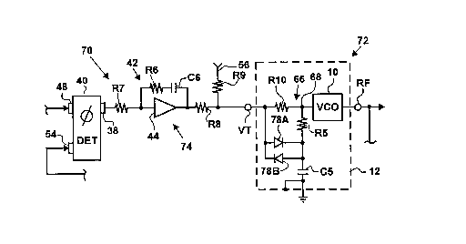
Referring now to FIGURE 6, a reduced IFM phase locking oscillator 70
includes components that are like-numbered and like-named with those in
CA 02299133 2000-02-23
14
FIGURE 5, except that the phase locking oscillator 70 includes a reduced IFM
voltage-controlled oscillator, variable frequency-deviation-sensitivity
voltage-
controlled oscillator, or radio frequency oscillator, 72 in a forward path 74
and
except as will be discussed.
The reduced IFM VCO 72 includes the VCO 10, the input voltage
terminal VT, the output frequency terminal RF, the ac voltage divider 66, and
diodes 78A and 78B.
Referring now to FIGURES 5 and 6, in the FIGURE 5 embodiment the
charge path from the integrator 42 to the capacitor C5 is via the resistor R8,
the
resistor R10, and the resistor R5. In the steady stage condition, an output
voltage of the integrator 42 is the same as a voltage of the capacitor C5.
However, at turn-on or channel change, they can differ by several volts.
Referring now to FIGURE 6, if the output voltage of the integrator 42 is
greater than a charge voltage on the capacitor C5 by more than 0.7 volts, the
diode 78A will conduct. Or, if a Schottky diode is used, and this forward
voltage difference is more than 0.3 volts, the diode 78A will conduct. When
the diode 78A conducts, the charge path from the integrator 42 to the
capacitor
C5 includes only the resistor R8.
Typical values of the resistors R8, R10, and R5 are 2.2k ohms, 4.7k
ohms, and 2.2k ohms, respectively, for a total of 9.1 k ohms. Therefore
whenever a forward voltage differential exists that causes the diode 78A to
conduct, the phase locking process is speeded by 9.1 k divided by 2.2k, or
approximately four times.
In like manner, when, due to a channel change, a voltage charge of the
capacitor C5 is more than 0.7 volts greater than an output of the integrator
42,
this reverse voltage differential causes the diode 78B to conduct, thereby
increasing the speed of discharge of the capacitor C5 by approximately four
times.
However, when either a forward or reverse voltage differential is lower
than those which will cause one of the diodes, 78A or 78B, to conduct, the ac
CA 02299133 2000-02-23
voltage divider 66 functions as described in conjunction with FIGURES 2 and 5.
That is, the VCO 72 functions at a reduced frequency-deviation-sensitivity,
thereby attenuating voltage spikes and resultant incidental frequency
modulation.
5 Referring now to FIGURE 7, a reduced IFM phase locking oscillator 80
includes components that are like-numbered and like-named with those in
FIGURES 5 and 6, except that the phase locking oscillator 80 includes a
reduced IFM voltage-controlled oscillator, or variable frequency-deviation-
sensitivity voltage-controlled oscillator, or radio frequency oscillator, 82
in a
10 forward path 84 and except as will be discussed.
The reduced IFM VCO 82 includes the VCO 10, the input voltage
terminal VT, the output frequency terminal RF, the ac voltage divider 66, an
npn transistor, or active solid state device, 88A, and a pnp transistor, or
active
solid state device, 88B.
15 When the integrator 42 produces a frequency-control voltage that
exceeds a charge on the capacitor C5, and this forward voltage differential
causes a voltage to be applied to a base B of the npn transistor 88A that is
approximately 0.7 volts greater than a voltage placed on an emitter E, the
transistor 88A conducts, communicating a voltage source from a supplementary
voltage terminal ST to the capacitor C5, greatly increasing both a speed of
charging the capacitor C5 and the speed of phase locking.
With values of the resistors R8, R10, and R5 as specified for the
FIGURE 5 embodiment, and assuming a ratio,Q of collector to base current for
the transistor 88A to be 25.0, the increase in phase locking speed provided by
the transistor 88A is equal to the total resistance of the resistors R8, R10,
and
R5, divided by the resistance of the resistor R5, with the quotient multiplied
by
~3 = (9.1 - 2.2) x 25 = approximately 100.
In like manner, when a charge on the capacitor C5 is greater than a
frequency-control voltage generated by the integrator 42, the pnp transistor
88B
conducts, discharging the capacitor C5 to a ground faster by approximately 100
times than current would flow through the resistors R5, R10, and R8 back to
the integrator 42.
CA 02299133 2000-02-23
16
Referring now to FIGURE 8, a reduced IFM phase locking oscillator 90
includes components that are like-numbered and like-named with those in
FIGURES 5, 6, and 7 except that the phase locking oscillator 90 includes a
reduced IFM voltage-controlled oscillator, or radio frequency oscillator, 92
in a
forward path 94, and except as will be discussed.
The reduced IFM VCO 92 includes the VCO 10, the input voltage
terminal VT, the supplementary voltage terminal ST, the output frequency
terminal RF, a PROM 96, a D/A converter 98, a voltage divider, or proportional
combiner, 100, and a conductor bus 102 for conducting digital commands to
the PROM 96.
The proportional combiner 100 includes the resistor R10 and the
resistor R5 which are series connected between the input voltage terminal VT
and the supplementary voltage terminal ST.
Assuming that the supplementary voltage terminal ST is at
ground potential, the resistors R10 and R5, which may have values of 4.7k and
2.2k, respectively, function as a voltage divider, thereby reducing a
frequency-
control voltage supplied by the integrator 42, thereby reducing a frequency-
deviation-sensitivity of the VCO 10 as a function of R8, R10, and R5
resistances, and thereby attenuating both voltage spikes and resultant
incidental
frequency modulation.
When the PROM 96 and the D/A converter 98 supply a channelizing
voltage to the supplementary voltage terminal ST, and this channelizing
voltage
is insufficient to phase lock the phase locking oscillator 90, the integrator
42
provides whatever magnitude of frequency-control voltage that is required to
achieve phase lock.
If resistances of the resistors, R10 and R5, were equal, then the
proportional combiner 100 would average the channelizing voltage with the
frequency-control voltage, and would apply that average to the VCO 10.
However, the resistance of the resistor R10 is greater than that of the
resistor R5. Therefore, voltages applied to the input voltage terminal VT and
the supplementary voltage terminal ST are proportionally combined, or
proportionally averaged. A voltage applied to the input voltage terminal VT
will be reduced more than one-half of the difference between the two voltages,
CA 02299133 2000-02-23
17
and a voltage applied to the supplementary voltage terminal ST will be reduced
less than one-half of the difference between the two voltages.
Because of the dividing, or proportional combining, function of the
voltage divider 100, both electrical noise and resultant incidental frequency
modulation are reduced. Further, because the PROM 96 and the D/A converter
98 provide a supplementary voltage, that is preferably a channelizing voltage,
the maximum capture range of the phase locking oscillator 90 is unattenuated
and phase locking is extremely rapid.
Preferably, the PROM 96 is loaded with channelizing information that
approximates phase lock for each channel that is to be accessed. Then, when a
channelizing selection is transmitted to the PROM 96 by the conductor bus
102, digital information in the PROM 96 is delivered to the D/A converter 98
which will produce a channelizing voltage that almost achieves phase lock
without waiting for the integrator 42 to generate the channelizing voltage.
The phase locking oscillator 90 achieves phase lock rapidly, not only
because of a means 104 for supplying a supplementary voltage or a
channelizing voltage to the supplementary voltage terminal ST, but also
because the capacitor C5 of FIGURES 5-7 has been eliminated, thereby
obviating the time required to charge and discharge a capacitor, such as the
capacitor C5 of FIGURES 5-7. The means 104 for supplying a supplementary
voltage includes the PROM 96 and the D/A converter 98.
Referring now to FIGURE 9, a reduced IFM phase locking oscillator
110 includes components that are like-numbered and like-named with those in
FIGURE 8, except that the phase locking oscillator 110 includes a reduced IFM
voltage-controlled oscillator, or radio frequency oscillator, 112 in a forward
path 1 14.
The VCO 112 includes the prior art VCO 10, the proportional
combiner 100, an UP comparator 116A, a DOWN comparator 116B, an
Up/Down counter 1 18, a clock 120, and the D/A converter 98. The
comparator 1 16A, the comparator 1 16B, the Up/Down counter 1 18, the clock
120, and the D/A converter 98 provide a means 122 for supplementing a
frequency-control voltage supplied to the input voltage terminal VT. The
CA 02299133 2000-02-23
18
supplementing means 122 is a digital integrator whose integration speed
depends upon the clock 120.
Selection of a given channel is achieved by selective adjustment of the
divider 52 of FIGURE 3, thereby changing a frequency fed back to the phase
detector 40 of FIGURES 3 and 9. For the following discussion, assume that a
frequency-control voltage of the integrator 42 of FIGURE 9 is at approximately
zero volts, and assume that an output of the D/A converter 98 is zero volts.
As the integrator 42 starts to generate a frequency-control voltage, the
frequency-control voltage is proportionally combined with the zero volts of
the
D/A converter 98. This proportional combining is a function of the resistances
of the resistors R10 and R5, thereby resulting in a reduced frequency-
deviation-
sensitivity of the VCO 92.
When the frequency-control voltage reaches a predetermined
magnitude, as determined by selective adjustment of the comparator 1 16A, an
UP signal is produced, and the Up/Down counter 118 starts to count. As the
count of the Up/Down counter 1 18 increases, the D/A converter 98 develops a
supplementary voltage, and this supplementary voltage is proportionally
combined with the frequency-control voltage.
This process continues until phase lock occurs. At phase lock the
supplementary voltage will be between limits set by the comparators 1 16A and
1 16B.
Therefore, the reduced IFM VCO 112 includes means, comprising the
proportional combiner 100, for reducing the frequency-deviation-sensitivity of
the VCO 10, the means 122 for supplementing the frequency-control voltage,
thereby restoring a capture range and a maximum frequency range, and means,
comprising the proportional combiner 100, for proportionally combining the
two voltages.
As defined herein, a frequency-control voltage is a voltage that is
developed by an integrator, such as the integrator 42, although a modulation
voltage that is applied to the modulation conductor 56 may also be considered
to be a frequency-control voltage. If a frequency-control voltage, or a
supplementary voltage, is sufficient in magnitude to approximately phase lock
a
CA 02299133 2000-02-23
19
phase locking oscillator 30, 60, 70, 80, 90, or 1 10 for a selected channel,
then
that voltage is a channelizing voltage.
In summary, the present invention provides phase locking oscillators
60, 70, 80, 90, and 110 in which incidental frequency modulation is reduced
or attenuated. The means for reducing incidental frequency modulation resides
in the VCOs 62, 72, 82, 92, and 112 of the present invention, which are a
subcombination of the phase locking oscillators 60, 70, 80, 90, and 110.
More particularly, the VCOs 62, 72, 82, 92, and 112 include means,
66 or 100, for reducing a frequency-deviation-sensitivity by reducing a
frequency-control voltage, thereby reducing electrical noise and voltage
spikes.
Reducing noise and/or voltage spikes results in attenuation of incidental
frequency modulation. Therefore, it is correct to say that embodiments of the
phase locking oscillators 60, 70, 80, 90, and 110, and embodiments of the
VCOs 62, 72, 82, 92, and 1 12 include means for reducing, or attenuating,
incidental frequency modulation.
In the VCOs 62, 72, and 82, the means 66 for reducing the frequency-
deviation-sensitivity is dependent upon a frequency of a frequency-control
voltage, and the frequency-deviation-sensitivity is reduced when a frequency
of
the frequency-control voltage is above a predetermined frequency. In contrast,
in the VCOs 92 and 112, the reduction of the frequency-deviation-sensitivity
is
continuous.
In the VCOs 62, 72, and 82, the means for reducing the frequency-
deviation-sensitivity, and incidental frequency modulation, comprises the ac
voltage divider 66. In the VCOs 92 and 1 12, the means for reducing the
frequency-deviation-sensitivity is the voltage divider, or proportional
combiner,
100.
Whether the ac voltage divider 66 or the proportional combiner 100 is
used, the means for reducing the frequency-deviation-sensitivity includes the
series-connected resistors R10 and R5 and includes the VCO 10 being
connected at the rate change node 68, of the series-connected resistors R10
and
R5, as shown in FIGURES 5-9. The resistors R10 and R5 of the ac voltage
divider 66 also function as a means for proportionally combining.
CA 02299133 2000-02-23
The resistors, R10 and R5, reduce a frequency-control voltage, as
developed by the integrator 42, to a reduced frequency-control voltage at the
rate change node 68. When reference is made to supplementing the frequency-
control voltage, it should be understood to mean supplementing the reduced
5 frequency-control voltage.
As defined herein, a frequency-deviation-sensitivity of a VCO is
reduced if a capture range, or maximum frequency locking range, has been
reduced to one half of a desired frequency locking range. Or, a frequency-
deviation-sensitivity is reduced if it is necessary to provide means for
restoring,
10 or partially restoring, a frequency-deviation-sensitivity to restore a
desired
portion of a reduced capture range of a phase locking oscillator or to restore
a
desired portion of a maximum frequency range of a voltage-controlled
oscillator. Or, a frequency-deviation-sensitivity is reduced if it is
necessary to
provide means for supplementing a frequency-control voltage that is supplied
to
15 a VCO to restore a desired portion of a reduced capture range of a phase
locking oscillator or to restore a desired portion of a reduced maximum
frequency range of a voltage-controlled oscillator.
In the VCOs 62, 72, and 82, the means for restoring the capture range,
or maximum frequency locking range, is means for restoring the frequency-
20 deviation-sensitivity of the VCOs 62, 72, and 82. More particularly, in the
VCOs 62, 72, and 82, the frequency-deviation-sensitivity is restored when a
frequency of the frequency-control voltage drops below a predetermined
frequency. Further, the means for restoring frequency-deviation sensitivities
is
the capacitor C5 of the ac voltage divider 66.
In the embodiments of FIGURES 8 and 9, which use the VCOs 92 and
112, respectively, the means for restoring the capture range, or maximum
frequency locking range, comprises the means 104 or 122 for supplementing
the frequency-control voltage that is supplied by the integrator 42.
In the phase locking oscillator 90 of FIGURE 8, the VCO 92 thereof
includes means 104 for supplementing the frequency-control voltage, and the
means 104 includes the PROM 96 and the D/A converter 98.
In the phase locking oscillator 110 of FIGURE 9, the VCO 112 includes
the means 122 for supplementing the frequency-control voltage, and the means
CA 02299133 2000-02-23
21
122 includes the comparators 116A and 116B, the Up/Down counter 118, the
clock 120, and the D/A converter 98.
As disclosed herein, the maximum frequency range of the radio
frequency oscillators, 62, 72, 82, 92, and 112 for a maximum frequency control
voltage can be fully restored, and a capture range for the phase locking
oscillators 60, 70, 80, 90, and 110 can be fully restored. However, in some
circumstances, it may be desirable to restore only one-half, or some other
portion, of a reduced maximum frequency range and/or a reduced capture
ran ge.
In the phase locking oscillators 60, 70, and 80, reducing the frequency-
deviation-sensitivity of the VCO, 62, 72, or 82, slows phase locking because
of
inclusion of the capacitor C5 and the time that is required for the integrator
42
to charge the capacitor C5. The VCOs 72 and 82 of FIGURES 6 and 7,
respectively, include means for increasing the speed of phase lock.
In the phase locking oscillator 70 of FIGURE 6, and the VCO 72
thereof, the means for increasing the speed of phase locking comprises the
diodes, 78A and/or 78B, bypassing the resistors R10 and R5 as a function of a
forward or reverse voltage differential. Stated another way, the diodes, 78A
and 78B, provide means for limiting the reducing of the frequency-deviation-
sensitivity. The diodes, 78A and 78B, limit the reduction in frequency-
deviation-sensitivity to voltages below their threshold.
Stated still another way, the diode 78A develops a supplementary
voltage, or an other voltage, that is a function of the frequency-control
voltage.
The resistors R10 and R5 proportionally combine the supplementary voltage
with the frequency-control voltage that has been reduced by the resistors, R10
and R5, thereby accelerating changing a charge on the capacitor C5, and
thereby increasing the speed of phase locking as a function of a forward
voltage
differential. Thus, the diode 78A is a means for providing a supplementary
voltage, means for increasing current flow into the capacitor C5, means for
accelerating changing a charge on the capacitor C5, and means for increasing a
speed of phase locking.
In a similar manner, the diode 78B is a means for increasing current
flow from the capacitor C5 back to the input voltage terminal VT, and a means
CA 02299133 2000-02-23
22
for increasing the speed of phase locking by communicating the capacitor C5
back to the integrator 42 as a function of a reverse voltage differential.
In the phase locking oscillator 80 of FIGURE 7, the VCO 82 thereof
includes means for increasing the speed of phase locking, and this means
includes the transistors, 88A and/or 88B.
That is, the transistor 88A provides means for communicating a
supplementary voltage, or an other voltage, to the capacitor C5 as a function
of
the forward voltage differential, thereby increasing current flow to the
capacitor
C5, and accelerating changing a charge on the capacitor C5 by increasing
current flow thereto, thereby providing a means for increasing phase locking
speed.
In like manner, the transistor 88B provides means for discharging the
capacitor C5 to ground as a function of the reverse voltage differential,
thereby
providing a means for increasing changing a charge on the capacitor C5, and
thereby providing a means for increasing the speed of phase locking.
In the phase locking oscillators, 90 and 110, of FIGURES 8 and 9, and
the IFM VCOs, 92 and 1 12, reducing the frequency-control voltage by the
voltage divider 100 results in reducing a maximum frequency range of the
voltage-controlled oscillator 92 for a maximum frequency-control voltage, and
results in reducing a capture range of the phase locking oscillators, 90 and
110.
However, the VCOs 92 and 112 include a means for developing and
proportionally combining a supplementary voltage, or an other voltage, with
the reduced frequency-control voltage, thereby restoring both the maximum
frequency range and the capture range.
In the VCO 92 of FIGURE 8, the means for providing a supplementary
voltage comprises means 104 for supplementing a frequency-control voltage of
the integrator 42 with an other voltage which is preferably a channelizing
voltage. In the phase locking oscillator 90, the means 104 for supplying the
channelizing voltage includes the PROM 96 and the D/A converter 98. The
channelizing voltage, as selected for the desired channel, drives an output
frequency of the VCO 92 to approximate phase lock much faster than the
integrator 42 can develop a channelizing voltage. That is, the PROM 96
CA 02299133 2000-02-23
23
provides means for nonvolatilely storing a preselected voltage, or a
channelizing voltage.
In the VCO 112 of FIGURE 9, the means for providing a supplementary
voltage, or another voltage, comprises means 122 for supplementing the
reduced frequency-control voltage with a supplementary voltage that is
generated from the frequency-control voltage. This supplementary voltage is
developed, or generated, by the comparators, 116A and 116B, the clock 120,
the Up/Down counter 1 18, and the D/A converter 98 when the frequency-
control voltage is outside either of two predetermined limits set by the
comparators, 1 16A and 1 16B.
As the frequency-control voltage and the supplementary voltage are
proportionally combined by the voltage divider 100, the proportionally-
combined voltage reaches a phase locking voltage for a given channel faster
than the integrator 42 could develop a frequency-control voltage that would
achieve phase lock.
Referring now to FIGURES 5-9, the resistors R10 and R5 provide means
for proportionally combining the frequency-control voltage with an other
voltage, such as a charge voltage on the capacitor C5, or a supplementing
voltage, such as a channelizing voltage. As is well known to those skilled in
the art, two voltages may be combined by summing, or otherwise combining.
And, two voltages may be summed, or otherwise combined, in direct
proportion or in any desired proportion. However, in the present invention,
preferably the two voltages are proportionally combined, with the
supplementary voltage predominating.
As taught herein, the diode 78A, the transistor 88A, the PROM 96 with
the D/A converter 98 that is included in the means 104, and the Up/Down
counter 1 18 with other components 98, 1 16A, 1 16B, 120 that are included in
the means 122, all provide means for providing, developing, or generating an
other voltage, or a supplementary voltage.
Whereas, in the embodiment of FIGURE 5, method and apparatus are
provided for restoring a reduced frequency-deviation-sensitivity of a radio
frequency oscillator 62 and a phase locking oscillator 60 as a function of a
frequency of the frequency-control voltage, in FIGURES 6-9, rather than
CA 02299133 2000-02-23
24
restoring a frequency-deviation-sensitivity, means 78A, 88A, 96, or 1 18 is
provided for restoring the maximum frequency range of a radio frequency
oscillator 72, 82, 92, or 1 12, and for restoring the capture range of a phase
locking oscillator 70, 80, 90, or 110.
Whereas, in the embodiment of FIGURE 5, the frequency-deviation-
sensitivity was restored as a function of a frequency of the frequency-control
voltage, in the embodiments of FIGURES 6-9, a maximum frequency range of a
radio frequency oscillator 72, 82, 92, or 1 12 and a capture range of a phase
locking oscillator 70, 80, 90, or 1 10 are restored irrespective of the
reduced
frequency-deviation-sensitivity, and irrespective of a frequency of the
frequency-
control voltage.
Further, whereas the maximum frequency range of the radio frequency
oscillator 62 of FIGURE 5 and the capture range of the phase locking
oscillator
60 are both restored as a function of a frequency of the frequency-control
voltage, the maximum frequency range of the radio frequency oscillators 72,
82, 92, and 112 and the capture range of the phase locking oscillators 70, 80,
90, and 110 of FIGURES 6-9 are restored by proportionally combining an other
voltage with the reduced frequency-control voltage.
Means for providing the other voltage may include the diode 78A, the
transistor 88A, the PROM 96, or the counter 1 18, as taught herein, or any
other
suitable device or schematic.
While an attenuation ratio of 10 to 1 has been given as an example for
the VCO 20 of FIGURE 2, a roll-off frequency of 1.59 Hz has been discussed
for the VCO 20, and a loop frequency of 60 Hz has been used as an example,
it should be realized that these specifics are merely examples, and that those
skilled in the art will be able to develop other variable frequency-deviation-
sensitivity VCOs, other phase locking loops using these improved VCOs, and
other electrical devices in accordance with apparatus, methods, and principles
disclosed herein.
Further, while specific apparatus and methods have been disclosed in
the preceding description, and while part numbers have been inserted
parenthetically into the claims to facilitate understanding of the claims, it
should
be understood that these specifics have been given for the purpose of
disclosing
CA 02299133 2000-02-23
the principles of the present invention, and that many variations thereof will
become apparent to those who are versed in the art. Therefore, the scope of
the present invention is to be determined by the appended claims, and without
any limitation by the part numbers inserted parenthetically in the claims.
5 INDUSTRIAL APPLICABILITY
The present invention is applicable to phase locking oscillators, voltage-
controlled oscillators, and other electronic equipment in which voltage spikes
and other electrical noise tend to produce unacceptable levels of incidental
frequency modulation.