Note: Descriptions are shown in the official language in which they were submitted.
CA 02299296 2000-02-08
WO 99/09682 1 PCT/SE98/01346
OPTICAL TRANSIvI1TTER SYSTEM AND METHOD
TECHINICAL FIELD OF THE INVENTION
The present invention relates to an optical duobinary
transmitter system and method using optical intensity
modulation.
DESCRIPTION OF RELATED ART
At high bit rates, the chromatic dispersion in standard single
mode fibers (SSMF) limits the transmission distance in the 1550
nm window. There has been a number of different methods proposed
to overcome this limitation of which the most common are pre-
chirped modulators, dispersion compensating fibers, chirped
Bragg gratings, mid-span spectral inversion, and special signal
formats such as dispersion supported transmission and duobinary
transmission.
Duobinary transmission has been investigated for modulators
showing no or very little chirp, i.e. a2z 0, see, e.g. Gu et
al., 10 Gbit/s unrepeatered three-level optical transmission
over 100 km of standard fiber, Electron. Lett., Vol. 29, No. 25,
1993, pp. 2209-2211 and May et al., Extended 10 Gbit/s fiber
transmission distance at 1538 nm using a duobinary receiver,
IEEE Phot. Technol. Lett., Vol. 6, No. 5, 1994, pp 648-650. The
chirp parameter a is defined as
acp
at
a 1 aP
2Pat
where 9 is the phase and P the intensity of the optical signal.
CA 02299296 2000-02-08 -
WO 99/09682 2 PCT/SE98/01346
The duobinary signal is DC-free and its transmission spectrum is
narrower than the spectrum of the binary signal. If the
duobinary signal is modulated on a carrier, the modulated signal
will behave as a double sideband signal with suppressed carrier.
The main benefit with duobinary transmission is that the
transmission spectrum is reduced compared to ordinary binary
transmission. In a dispersion limited system, the transfer
length is inversely proportional to the square of the bandwidth
of the transmission spectrum. This means that if the
transmission spectrum is reduced to one half the transfer length
is quadrupled.
Further, since the carrier frequency is suppressed in the
duobinary transmission spectrum, the limitation for the output
optical power due to stimulated Brillouin scattering in the
fiber can be relaxed.
Optical duobinary transmission can be considered as a three-
level signaling scheme which can be detected with an ordinary
binary receiver. The normal marks in binary transmission are "0"
and "1", whether the marks in duobinary transmission are "-1",
"0", and "1", In the optical case, the duobinary marks are
modulated as "-4P", "0", and "4P", where P is the optical peak
power. These will be interpreted as "P", "0", and "P" in an
ordinary opto-electric quadratic detector.
A common way to construct an optical duobinary transmitter is to
make use of a double-electrode Mach-Zehnder (DEMZ) modulator,
see, e.g. the US patent 5,543,952 or the international
application WO 95/29539. The DEMZ-modulator has also been
proposed for adjustable chirp applications, see A.H. Gnauck et
CA 02299296 2000-02-08
3
WO 99/09682 PCT/SE98/01346
al., Dispersion penalty reduction using an optical modulator
with adjustable chirp, IEEE Phot. Technol. Lett., Vol. 3, No.
10, 1991, pp 916-918, as well as simultaneous 2:1 multiplexing
and modulation, see P.B. Hansen et al., A dual-drive Ti:LiNbO3
Mach-Zehnder Modulator used as an optoelectric logic gate for 10
Gbit/s simultaneous multiplexing and modulation, IEEE Phot.
Technol. Lett., Vol. 4, No. 6, 1992, pp 592-593.
A typical optical duobinary transmitter based on a DEMZ-
modulator according to prior art is explained with reference to
the layout as shown in fig. 1.
The input signal of the transmitter is an electrical binary
signal S1 and its complement S2 = S1. Each of these signals is
fed through a binary-to-duobinary encoder 1, 3 and an AC-
amplifier 5, 7. The resulting duobinary, i.e. three-level,
signals S3, S4 are amplified and then used as driving signals of
the electrodes of the modulator 9.
Continuos light from a laser diode 11 is coupled into the
modulator 9 and split into two components in the Y-junction 9a
of the left part of the modulator. The light in the two branches
9b, 9c of the modulator will then undergo positive or negative
phase shift in the middle part of the modulator, the phase shift
being controlled through the linear electro-optic effect by the
applied voltage, i.e. the duobinary driving signals S3, S4, of
the electrodes of the modulator. The phase shift in the upper
branch is controlled by the upper electrode, and the phase shift
in the lower branch is controlled by the lower electrode. The
electrodes are supplied by bias voltage 13 in order to obtain
the same phase shift in the two branches when no driving signals
are applied to the electrodes.
CA 02299296 2000-02-08
WO 99/09682 4
PCT/SE98/01346
The light in the two branches are then combined coherently in
the Y-junction 9d in the right part of the modulator. If there
is a 0 phase shift between the components, all light will be
injected in the outgoing optical waveguide. If there is a 180
phase shift, no light will be injected in the outgoing
waveguide. In the latter case, the light will be radiated into
the modulator.
The coding procedure for duobinary transmission is very simple.
In fig. 2 is shown the binary-to-duobinary encoder 1 which
converts the binary signal Si into a duobinary signal S3 by
using two flip-flops 15, 17 and a clock pulse 19. The flip-flops
have binary output signals S5, S6, which are equal to the input
binary signal but shifted one bit and two bits, respectively.
The binary output signals S5, S6 are then fed through an adder
21 with the following function
S3 = S5 + S6 - 1
thus, generating the duobinary signal S3. In fig. 3 is shown an
example of the output signal S3 and the encoding intermediate
signals S5, S6 for duobinary modulation of the binary signal Si.
It may be observed that a direct transition between the marks
"-1" and "1" never occurs in duobinary modulation. The binary-
to-duobinary encoder 3 is constructed and functioning likewise
with the only difference that the input signal S2 is the
complement of the binary signal Si.
The introduced phase shift in the upper and in the lower branch
of the optical duobinary modulator for each of the marks are
indicated in fig. 4a. The logical "1" mark corresponds to a
light pulse with full amplitude and a 0 phase shift, the "0"
CA 02299296 2000-02-08
WO 99/09682 5 PCT/SE98/01346
mark corresponds to no light pulse at all as the two components
are opposite in phase and cancel each other out, and the "-1"
mark corresponds to a light pulse with full amplitude and a 1800
phase shift.
Fig. 4b shows a polar graph (amplitude vs phase) of the locus of
the optical output signal (thick solid line) and the location of
each of the duobinary marks (dots). The phase of the optical
output signal does not vary on its way between the marks.
Therefore, dcp/dt = 0 and a 0 according to the formula
presented above.
The main problem with a duobinary transmitter as described is
that the chromatic dispersion still limits the transmission
distance and may be a problem for long haul fiber transmission
systems.
SLJMMARY OF THE INVENTION
An object of the present invention is to provide an optical
duobinary transmitter with an improved performance in terms of
dispersion immunity.
This object among others is fulfilled by an inventive optical
duobinary transmitter system and method, which introduces a
blue-shift frequency chirp.
The inventive system and method comprises an input terminal, a
driving circuit, a double electrode optical modulator,
particularly of the Mach-Zehnder type, and an output terminal.
The input terminal is arranged to receive a first binary signal
and the driving circuit, which is connected to said input
terminal, is arranged to convert the first binary signal into a
CA 02299296 2000-02-08 -
WO 99/09682 6 PCT/SE98/01346
second and a third binary signal. The double electrode optical
modulator is connected to the driving circuit in such a way that
its upper and lower electrode may be driven by said second and
third binary signal, respectively, said modulator being further
arranged to modulate the amplitude and phase of an optical
carrier according to the binary driving signals so as to provide
an optical duobinary signal corresponding to said first binary
signal and with a predetermined negative modulation chirp
parameter. Finally, the output terminal, which is connected to
the optical modulator, is arranged to feed an optical
transmission line with the modulated optical duobinary signal.
Preferably, the driving circuit comprises a first and a second
logical gate whose outputs are connected to the respective
electrode of the double electrode optical modulator. The logical
gates may be an AND- or a NAND-gate and an OR- or a NOR-gate,
respectively.
The logical gates are driven by two binary signals that may be
the outputs of either a demultiplexer or two flip-flops, which
in turn is/are driven by the first binary signal.
The demultiplexer would be arranged to demultiplex the first
binary signal, e.g. ABCDEFGH, into two binary signals, e.g.
AACCEEGG* and *BBDDFFHH, respectively, where * denotes an
undefined signal mark.
The two flip-flops would be serially connected and arranged to
demultiplex the first binary signal, e.g. ABCDEFGH, into two
binary signals, e.g. *ABCDEFGH and **ABCDEFGH, respectively.
CA 02299296 2000-02-08
WO 99/09682 7 PCT/SE98/01346
Furthermore, the second and the third binary signals may be
arranged to be amplified prior to driving the electrodes of the
modulator.
The double electrode optical modulator is preferably arranged to
introduce the same phase shift of the optical carrier components
led through the two branches for a given applied voltage. The
three optical duobinary marks may be provided as no light pulse
(or a light pulse with a very low amplitude), a first light
pulse with a high amplitude and a second light pulse with a high
amplitude, the two latter light pulses being opposite in phase
to each other.
The double electrode optical modulator may further be arranged
to provide modulated light with a phase cp having a negative time
derivative, i.e. dcp/dt < 0, when the intensity of the modulated
light is being raised.
In another embodiment of the present invention the upper and
lower electrodes of the modulator are driven by a first and a
second quasi-ternary signal. Preferably, the first and second
quasi-ternary signals are provided with non-equidistant marks,
e.g. "1", "0.25", "0" and "1", "0.75", "0", respectively, in
order to obtain a predetermined amount of negative chirp, e.g.
a3dB = -0.5.
An advantage of the invention is that it may into some extent
compensate for dispersion in dispersive systems such as a fiber-
optic system operating at 1550 nm in standard single mode
fibers.
CA 02299296 2000-02-08
WO 99/09682 8 PCT/SE98/01346
Another advantage is that it needs a lower receiver sensitivity
for a given transmission distance as compared with the
transmitter system described in prior art.
Still another advantage of the invention is that when the AC-
amplifiers amplify binary signals instead of duobinary signals
the demands on them are relaxed.
Yet another advantage is that the invention is easy and simple
to implement and uses a minimum of coding electronics.
BRIEF DESCRIPTION OF THE DRAWINGS
The present invention will become more fully understood from the
detailed description given hereinbelow and the accompanying
Figs. 5-11 which are given by way of illustration only, and thus
are not limitative of the present invention.
Fig. 1 shows an optical duobinary transmitter according to prior
art.
Fig. 2 shows an encoder circuit for converting a binary signal
into a duobinary signal according to prior art.
Fig. 3 illustrates one example of an output signal and encoding
intermediates for encoding of a binary signal according to prior
art.
Fig. 4a illustrates phase shifts in the upper and in the lower
branch of the optical duobinary transmitter of fig. 1 for each
of the duobinary marks.
Fig. 4b shows a polar graph of the locus of the optical output
signal and the location of each of the duobinary marks of the
duobinary transmitter of fig. 1.
CA 02299296 2000-02-08
WO 99/09682 9 PCT/SE98/01346
Fig. 5 shows an optical duobinary transmitter according to a
preferred embodiment of the present invention.
Fig. 6 illustrates an example of an output signal and encoding
intermediates for duobinary modulation of a binary signal by the
inventive optical duobinary transmitter of fig. 5.
Fig. 7a illustrates phase shifts in the upper and in the lower
branch of the inventive duobinary transmitter of fig. 5 for each
of the duobinary marks.
Fig. 7b shows a polar graph of the locus of the optical output
signal and the location of each of the duobinary marks of the
inventive duobinary transmitter of fig. S.
Fig. 8 shows an optical duobinary transmitter according to a
second preferred embodiment of the present invention.
Fig. 9 illustrates an example of output signal and encoding
intermediates for duobinary modulation of a binary signal by the
inventive optical duobinary transmitter shown in fig 8.
Fig. 10 shows receiver sensitivity for three different
modulation schemes according to prior art and one modulation
scheme according to the present invention as simulated for
different transfer lengths.
.Fig. lla illustrates phase shifts in the upper and in the lower
branch for each of the duobinary marks of an optical duobinary
transmitter driven by quasi-ternary signals according to a third
preferred embodiment of the present invention.
Fig. llb shows a polar graph of the locus of the optical output
signal and the location of each of the duobinary marks for an
CA 02299296 2000-02-08 -
WO 99/09682 10 PCT/SE98/01346
optical duobinary transmitter with phase shifts according to
fig. lla.
DETAILED DESCRIPTION OF EMBODIMENTS
The duobinary transmitter according to the present invention is
based on the DEMZ-modulator, but the modulation is completely
different compared to the modulation technique as described in
prior art.
A first preferred embodiment of the present invention will be
described with reference to fig. 5. An optical duobinary
transmitter comprises an input terminal 51, a driving circuit
53, a double electrode optical modulator 55, preferably a DEMZ-
modulator, and an output terminal 57.
The driving circuit is connected to the input terminal and
comprises a demultiplexer 59 and two logical gates 61, 63,
preferably an AND- and an OR-gate. The demultiplexer is arranged
to demultiplex an input binary signal Si into two binary signals
S7 and S8, each having half the bit-rate of the input binary
signal Si. In this case it is essential that these signals
change its marks out of phase to each other. For example, an
incoming signal sequence ABCDEFGH should be demultiplexed into
the sequences AACCEEGG* and *BBDDFFHH, where * denotes an
undefined signal mark.
If the demultiplexed signals S7 and S8 are already available at
the input terminal no demultiplexer is needed. In this case a
synchronization circuit (not shown in fig. 5), e.g. comprising
four flip-flops and the use of a clock pulse, may be arranged to
synchronize the demultiplexed signals and assure that they
change their marks out of phase to each other.
CA 02299296 2000-02-08
WO 99/09682 11
PCT/SE98/01346
The logical gates, of which each has the two binary signals S7
and S8 as inputs, generate two binary signals S9 and SIO which
in turn are used to drive the electrodes of the double electrode
optical modulator 55.
AC-amplifiers 65, 67 may be arranged to amplify the binary
signals S9 and S10, respectively, prior to driving the
electrodes of the modulator.
The optical double electrode modulator 55, whose electrodes are
supplied by bias voltage 69, is arranged to modulate the
amplitude and phase of an optical carrier, e.g. continuous light
from a laser diode 71, according to the binary driving signals
so as to provide an optical duobinary signal S3 corresponding to
the input binary signal Si and with a predetermined negative
modulation chirp parameter, i.e. a < 0. The output duobinary
signal S3 contains the same data information as the input binary
signal Si, but with a narrower transmission spectrum.
Finally, the output terminal 57 is connected to the optical
modulator and arranged to feed an optical transmission line (not
shown in fig. 5) with the modulated optical duobinary signal S3.
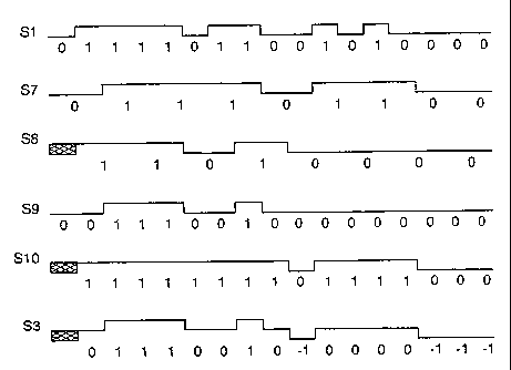
In fig. 6 is shown an example of the output duobinary signal S3
and the encoding intermediate signals S7, S8, S9 and S10 for
duobinary modulation of a binary signal SI according to the
present invention.
The double electrode optical modulator is preferably of the kind
that it introduces substantially the same phase shift Ocp of the
optical carrier light led through the two branches of the
modulator for a given voltage shift OV of the corresponding
driving signal, i.e. Acp/OV should be the same. This gives the
CA 02299296 2000-02-08
WO 99/09682 12 PCT/SE98/01346
best possibilities for obtaining a high-quality modulated
signal.
When being driven by the binary signals S9 and S.ZO,
respectively, the double electrode optical modulator is arranged
to provide the three optical duobinary signal marks "0", "i",
"-1" as substantially no light pulse, and two light pulses with
a high amplitude, but opposite in phase to each other.
in fig. 7a is indicated the introduced phase shift in the upper
and in the lower branch of the duobinary modulator for each of
the marks. The "0" mark corresponds to substantially no light
pulse at all as the two components are opposite in phase and
cancel each other out, the logical "1" mark corresponds to a
light pulse with full amplitude and a 0 phase shift, and the
"-1" mark corresponds to a light pulse with full amplitude and a
180 phase shift. It is assumed that the light in the upper
branch of the modulator undergoes negative phase shift and the
light in the lower branch undergoes positive phase shift when
the electrode voltage goes high.
Particularly, it may be observed from figs. 6 and 7a that the
marks of the binary signals S9 and S10, and consequently the
introduced phase shift of the upper and the lower branch of the
modulator, never change simultaneously. This is an essential
feature necessary for providing the desired properties of this
embodiment of the present invention.
Fig. 7b shows a polar graph (amplitude vs phase) of the locus of
the optical output signal (thick solid line) and the location of
each of the duobinary marks (dots).
CA 02299296 2000-02-08
WO 99/09682 13 PCT/SE98/01346
The upper arm of the interferometer is modulated between 0 and
180 using the first and the second quadrant of the polar
diagram, and the lower arm is modulated between 0 and -180
using the third and the fourth quadrant. The phase of the
optical output signal varies between 90 and 0 on its way
between the "0" and the "1" mark as indicated in the figure.
Therefore, dcp/dt < 0 when dP/dt > 0, which gives a < 0 according
to the formula presented in the description of related art.
Between the "0" and the "-1" mark the phase varies between -90
and -180 . Again, dcp/dt < 0 when dP/dt > 0, which gives a < 0.
Consequently, the optical modulator is arranged to provide
modulated light with a phase cp having a negative time
derivative, i.e. dcp/dt < 0, when the intensity of the modulated
light is being increased and a positive time derivative, i.e.
dcp/dt > 0, when the intensity of the modulated light is being
decreased.
For all traces the chirp parameter a is less than zero, which
means that blue-shift frequency chirp occurs. This frequency
chirp can to some extent compensate for dispersion in anomalous
dispersive systems such as fiberoptic systems operating at 1550
nm on SSMF. The chirp parameter a3dB is defined at half the
optical peak power and equals -1 in the embodiment as described.
This value is slightly higher than the optimum value.
The proposed inventive modulation scheme can be implemented with
very little additional electronics compared to a conventional
duobinary transmission link. At the transmitter side, the adder
may be substituted by two logical gates such as one AND-gate and
CA 02299296 2000-02-08
WO 99/09682 14 PCT/SE98/01346
one OR-gate. At the receiver side, no supplementary devices are
needed. A standard duobinary receiver may be used.
The benefits of the narrow frequency signal spectrum for
duobinary transmission and of the dispersion compensation
properties of chirped modulation are combined. Moreover, the AC-
amplifiers are in this case driven with binary signals. In
comparison to the traditionally duobinary modulation scheme, the
binary drive signals will relax the demands of the AC-
amplifiers.
Fig. 8 shows a second preferred embodiment of an optical
duobinary transmitter according to the present invention. This
transmitter is very similar to the one described above, the
driving circuit 73 being the only different part.
The driving circuit 73 comprises two serially connected D-flip-
flops 75, 77 and a clock pulse 79 instead of the demultiplexer.
The D-flip-flops are arranged to convert an input binary signal
Si into two binary output signals Sii and S13, respectively,
each having the full bit-rate of the input binary signal Si. In
this arrangement, an incoming signal sequence of ABCDEFGH is
converted into the two sequences *ABCDEFGH and **ABCDEFGH,
respectively, i.e. the binary output signals being equal to the
input binary pulse but shifted one bit and two bits,
respectively.
The logical gates 61, 63, of which in this embodiment each has
the two binary output signals S11 and S12 as inputs, generate
two binary signals S13 and S14 which in turn are used to drive
the electrodes of the double electrode optical modulator 55. The
signals S13 and S14 are identical with the signals S9 and S10
CA 02299296 2000-02-08
WO 99/09682 15 PCT/SE98/01346
provided that the logical gates are the same. Hence, the
modulators of the first and second preferred embodiment are
driven by identical signals and generate identical duobinary
signals. Consequently, a desirable blue-shift frequency chirp of
the modulated signal is obtained also in this embodiment.
In fig. 9 is shown an example of the output duobinary signal S3
and the encoding intermediate signals S11, S12, S13, and S14 for
duobinary modulation of a binary signal SI according to the
second preferred embodiment of the present invention.
Other possible driving circuits that are compatible with the
present invention use other type of logical gates. For instance,
using LiNbO3 as the wave guide medium of the modulator it is
possible to use any of the combinations listed in Table 1 with
appropriate choices of types of electrodes and biasing voltages.
Table 1.
1 x-cut AND OR
2 x-cut AND NOR
3 x-cut NAND OR
4 x-cut NAND NOR
5 y-cut AND NOR
6 y-cut NAND OR
It is possible to use inverted or non-inverted driving stages.
The principle of obtaining the binary driving signals is the
same.
CA 02299296 2000-02-08
WO 99/09682 16 PCT/SE98/01346
Other possible materials for the waveguides of the modulator are
semiconductor materials such as, e.g., InP. Using these
materials it is easier to provide modulators with the same Ocp/AV
for the two branches.
A theoretical comparison study has been performed of four
different modulation schemes:
i.Intensity modulation with no chirp
2.Intensity modulation with chirp
3.Duobinary modulation with no chirp
4.Duobinary modulation with chirp according to the invention
The first scheme comprises a DEMZ-modulator modulated on both
its electrodes with two synchronously binary signals. The
modulation scheme corresponds to the transition between the "1"
mark and the "0" mark of fig. 4b. The peak-to-peak drive voltage
is Vn/2 and the required slow-rate for the drive signal is
Vn/2T, where T is the time between the marks and Vn is the
voltage that shifts the phase of the light 180 .
In the second modulation scheme the DEMZ-modulator is modulated
on its upper electrode with a single binary signal. The scheme
corresponds to the transition between the "1" mark and the "0"
mark of fig. 7b. The peak-to-peak drive voltage is Vn and the
required slow-rate for the drive signal is Vn/T.
The third scheme comprises a DEMZ-modulator modulated on both
its electrodes with two synchronously three-level signals. The
modulation scheme coincides with the one described in related
art. The peak-to-peak drive voltage is Vn and the required slow-
rate for the drive signal is Vn/2T. In this case, a direct
CA 02299296 2000-02-08
WO 99/09682 17 PCT/SE98/01346
transition between the marks 111" and "-1", and vice versa never
occurs.
In the fourth modulation scheme the DEMZ-modulator is modulated
on both its electrodes with two binary signals that are out of
phase to each other. The modulation coincides with the one
depicted in the present invention. The peak-to-peak drive
voltage is Vn and the required slow-rate for the drive signal is
Vn/T. Neither in this scheme a direct transition between the
marks "1" and "-1", and vice versa occurs.
The performance of the four modulation schemes has been analyzed
by using a raised cosine type drive signal as input signal to
the DEMZ-modulator and a 4th order Bessel filter as receiver
filter optimized according to the ITU (International
Telecommunication Union) norm. The bit-rate was set to 10 Gbit/s
and the dispersion parameter for the fiber was D = 17 ps/nm/km
corresponding to an STM-64 (aynchronous Transfer Mode) system
operating at 1550 nm on SSMF. The fiber was modelled as a phase-
revolving filter with the transfer function
x 2 DL(w c - (0) 2
i
HswF (w ) _ e 47cc
where k is the wavelength, D the dispersion parameter, L the
transfer length, co,, the carrier frequency, w the signal
frequency, and c the velocity of light in vacuum.
Furthermore, a commercial erbium doped fiber amplifier (EDFA)
was used as a pre-amplifier at the receiver side (amplification
G = 29 dB and noise factor F 4.5 dB). The output signal from
CA 02299296 2000-02-08
WO 99/09682 18 PCT/SE98/01346
the EDFA was then filtered through a Fabry-Perot filter ( AX _
2.5 nm).
In fig. 10 is shown the result of the investigation in terms of
the receiver sensitivity in decibel vs the transfer length in
kilometers. The solid line corresponds to intensity modulation
with no chirp, the dashed line to intensity modulation with
chirp, the dotted line to duobinary modulation with no chirp,
and the dashed-dotted line to duobinary modulation with chirp
according to the invention. A bit-error-rate of i*10-9 is
assumed for the four different modulation schemes. As can be
seen in the figure the fourth modulation scheme, i.e. duobinary
modulation with chirp, shows the best performance for all
transfer lengths considered, i.e. 0-160 km.
In a third preferred embodiment of an optical duobinary
transmitter according to the present invention the driving
signals are quasi-ternary instead of binary. The chirp parameter
a3dS may hereby be optimized at the cost of a more complex
driving circuit. For example, if a chirp parameter of -0.5 at
the 3 dB point is desired, the acquired phase shift in the two
branches of the modulator shall have a ratio of 1:3. This is
realized by converting an input binary signal into two quasi-
ternary signals, the one driving the electrode of the upper
branch of the modulator having the three marks "1", "0.25" and
"0", and the one driving the electrode of the lower branch of
the modulator having the three marks "1", "0.75" and "0".
In fig. ila is shown the introduced phase shift in the upper and
in the lower branch of the duobinary modulator for each of the
marks. The "0" mark corresponds to substantially no light pulse
at all as the two components are opposite in phase and cancel
CA 02299296 2000-02-08
WO 99/09682 19 PCT/SE98/01346
each other out, the logical "1" mark corresponds to a light
pulse with full amplitude and a 0 phase shift, and the
"-1" mark corresponds to a light pulse with full amplitude and a
180 phase shift. It is assumed that the light in the upper
branch of the modulator undergoes negative phase shift and the
light in the lower branch undergoes positive phase shift when
the electrode voltage goes high.
It may be observed from lla that the marks of the quasi-ternary
signals, and consequently the introduced phase shift of the
light in the upper and the lower branch of the modulator, change
simultaneously in this embodiment.
Fig. lib shows a polar graph (amplitude vs phase) of the locus
of the optical output signal (thick solid line) and the location
of each of the duobinary marks (dots).
The new inventive system and method for duobinary transmission
as described in the present patent application combines the
narrow spectrum that duobinary transmission offers with the
dispersion compensation properties that chirped techniques
offer. In the theoretical study it is shown that a modulation
scheme according to one embodiment of the present invention
shows overall better performance in terms of dispersion immunity
compared to earlier known modulation techniques based on the
DEMZ-modulator.
According to the first described embodiments of the present
invention, the drivers for the DEMZ electrodes are driven with
binary signals instead of three-level signals. This will relax
the design demands of the driver circuits.
CA 02299296 2000-02-08
WO 99/09682 20 PCT/SE98/01346
According to the last described embodiments of the present
invention, the drivers for the DEMZ electrodes are driven with
quasi-ternary signals instead of ordinary duobinary signals. The
chirp parameter may hereby be optimized.
The invention being thus described, it will be obvious that the
same may be varied in a plurality of ways. Such variations are
not to be regarded as a departure from the scope of the
invention. All such modifications as would be obvious to one
skilled in the art are intended to be included within the scope
of the following claims.