Language selection

Search

Patent 2299714 Summary

Third-party information liability

Some of the information on this Web page has been provided by external sources. The Government of Canada is not responsible for the accuracy, reliability or currency of the information supplied by external sources. Users wishing to rely upon this information should consult directly with the source of the information. Content provided by external sources is not subject to official languages, privacy and accessibility requirements.

Claims and Abstract availability

Any discrepancies in the text and image of the Claims and Abstract are due to differing posting times. Text of the Claims and Abstract are posted:

  • At the time the application is open to public inspection;
  • At the time of issue of the patent (grant).
(12) Patent Application: (11) CA 2299714
(54) English Title: CIRCUIT PACK ADVANCED GUIDANCE INTO GUIDE SLOT AND CONNECTOR PROTECTION
(54) French Title: CARTE IMPRIMEE A DISPOSITIF DE GUIDAGE DANS LA FENTE ET DE PROTECTION DU CONNECTEUR
Status: Deemed Abandoned and Beyond the Period of Reinstatement - Pending Response to Notice of Disregarded Communication
Bibliographic Data
(51) International Patent Classification (IPC):
  • H05K 07/00 (2006.01)
  • H05K 07/14 (2006.01)
(72) Inventors :
  • GANGEMI, JOSEPH L. (United States of America)
  • HWANG, LIANG (United States of America)
  • LI, HSIAO C. (United States of America)
(73) Owners :
  • LUCENT TECHNOLOGIES INC.
(71) Applicants :
  • LUCENT TECHNOLOGIES INC. (United States of America)
(74) Agent: KIRBY EADES GALE BAKER
(74) Associate agent:
(45) Issued:
(22) Filed Date: 2000-02-29
(41) Open to Public Inspection: 2000-09-15
Examination requested: 2000-02-29
Availability of licence: N/A
Dedicated to the Public: N/A
(25) Language of filing: English

Patent Cooperation Treaty (PCT): No

(30) Application Priority Data:
Application No. Country/Territory Date
09/268,149 (United States of America) 1999-03-15

Abstracts

English Abstract


A circuit card wherein tabs extend beyond the forward
edge of the card and beyond the forward mating end of
connectors mounted to the card to provide protection to the
connectors and advanced guidance of the card into card cage
guide slots.


Claims

Note: Claims are shown in the official language in which they were submitted.


6
Claims:
1. A circuit card adapted to be inserted into a card
cage, the card cage having a pair of opposed parallel guide
slots for receiving opposed parallel side edges of the
circuit card, the circuit card having a forward edge
extending between the pair of side edges and a connector
secured to the circuit card between the pair of side edges
and extending forwardly beyond the forward edge of the card
for engagement with a complementary mating connector on a
backplane secured to the card cage, wherein the improvement
comprises:
a pair of tabs formed as part of the circuit card, each
of the tabs having an edge which is an extension of a
respective one of the pair of side edges and each of the tabs
extending forwardly beyond the connector between the
connector and the respective one of the pair of side edges;
whereby the pair of tabs are effective to provide
advanced guidance of the circuit card into the card cage
guide slots.
2. A circuit pack comprising:
a circuit board having a pair of opposed parallel side
edges and a forward edge extending between said pair of side
edges, said circuit board forward edge being recessed over a
portion of its length so as to provide a pair of forwardly
extending tabs each having as one side edge a portion of a
respective one of said pair of side edges and each having a
forward edge;
a connector secured to said circuit board along said
circuit board forward edge between said pair of tabs, said
connector having a forward mating end lying between said
circuit board forward edge and a line joining the forward
edges of said pair of tabs;

7
at least one circuit component mounted to said circuit
board; and
circuitry connecting said at least one circuit component
to said connector.
3. A circuit board having a pair of opposed parallel
side edges and a forward edge extending between said pair of
side edges, each of said pair of side edges extending
forwardly to a line orthogonal to said pair of side edges,
and said forward edge being recessed along a central portion
thereof rearwardly of said line so as to provide a pair of
tabs each extending forwardly to said line, with each of said
pair of tabs having a portion of a respective one of said
board side edges as one of its side edges.
4. The circuit board according to Claim 3 further
comprising:
a connector mounted to said circuit board along said
forward edge central portion, said connector having a forward
mating end between said forward edge central portion and said
line.

Description

Note: Descriptions are shown in the official language in which they were submitted.


CA 02299714 2000-02-29
Gangemi 1-2-1
CIRCUIT PACK ADVANCED GUIDANCE INTO GUIDE SLOT AND
CONNECTOR PROTECTION
Background Of The Invention
This invention relates to a circuit pack adapted for
insertion into a card cage guide slot and, more particularly,
to advanced guidance of the circuit pack during such
insertion and to protection of the circuit pack connector.
Modern electronic systems equipment, such as for
telecommunications purposes, is often constructed as modular
circuit packs inserted into guide slots of mechanical card
cages for engagement with a backplane mounted to the card
cage at the inward ends of the guide slots . Usually, the
packaging requirements for such systems results in a high
density of circuit packs, with minimum spacing between
circuit packs. Each circuit pack includes a circuit board,
at least one circuit component mounted to the circuit board,
a connector secured to the circuit board along a forward edge
of the board and circuitry connecting the circuit component
to the connector. In advanced technology packaging, the
surface of the connector may include conductive piece parts,
such as circuit pack grounding shields needed for
electromagnetic interference and/or improved signal quality,
that can cause shorting of an adjacent circuit pack already
installed in the card cage if the circuit pack being
installed is not properly aligned upon insertion into a card
cage guide slot. It would therefore be desirable to provide
some way of preventing such shorting without increasing the
spacing between adjacent circuit packs.
In addition, it has been found that inadvertent
mishandling of the circuit pack can result in damage to the
connector. It would also be desirable to provide protection
to the connector from such mishandling.

CA 02299714 2000-02-29
Gangemi 1-2-1
Summary Of The Invention
According to the present invention, the circuit board is
extended along opposed edges beyond the circuit pack
connector. The extensions provide advanced guidance of the
circuit card into a guide slot of the card cage, insuring
that the connector along the forward edge of the card is
properly spaced from an adjacent circuit pack. In addition,
the extensions provide protection to the connector from
inadvertent mishandling.
Brief Description Of The Drawings
The foregoing will be more readily apparent upon reading
the following description in conjunction with the drawings in
which like elements in different figures thereof are
identified by the same reference numeral and wherein:
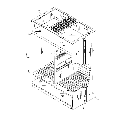
FIGURE 1 is a rear perspective view of a mechanical card
cage, without the backplane installed;
FIGURE 2 is a front view of the card cage shown in
Figure 1 with the backplane installed;
FIGURE 3 is a side view of a circuit pack having the
present invention incorporated therein; and
FIGURE 4 is an enlarged partial side view of the circuit
pack shown in Figure 3 showing the initial entry of the
circuit pack into a guide slot of the card cage.
Detailed Description
Referring now to the drawings, Figure 1 shows a card
cage, designated generally by the reference numeral 10, with
which the present invention finds utility. As is
conventional, the card cage 10 is typically mounted to an
equipment rack, by means of the flanges 12, and includes an
exterior metal enclosure 14. The card cage 10 includes

CA 02299714 2000-02-29
Gangemi 1-2-1 3
parallel spaced apart upper plate 16 and lower plate 18
secured to the enclosure 14. The upper and lower plates 16,
18 are substantially the same and provide a plurality of
parallel guide slots 20 for a plurality of circuit packs.
Illustratively, the plates 16, 18 are stamped and formed to
have cutouts with upturned edges to provide the guide slots
20 between adjacent upturned edges. A separator plate 22 may
be provided to which is secured a member 24 having opposed
flanges 25, 26 on which are formed guide slots 27 so that
smaller circuit packs may be accommodated in the card cage
10. As is conventional, mounted to the back of the enclosure
14 is a backplane 28, as shown in Figure 2. The backplane 28
is a planar circuit board having an array of connectors 30
secured thereto. The connectors 30 are so situated on the
backplane 28 that when a circuit pack is inserted into a pair
of opposed guide slots 20, the connector on the circuit pack
engages respective connectors) 30 upon being fully inserted
into the enclosure 14.
The problem which the present invention solves arises
due to the close spacing between adjacent guide slots 20. If
a circuit pack is not initially inserted at the correct angle
into a pair of guide slots, metal shielding on a circuit pack
connector can inadvertently contact circuitry on an adjacent
circuit pack.
Figure 3 illustrates a circuit pack, designated
generally by the reference numeral 32, in which is
incorporated the present invention. The circuit pack 32
includes a circuit board 34 having a pair of opposed parallel
side edges 36, 38, and a forward edge 40 extending between
the side edges 36, 38. Connector arrays 42 are secured to
the circuit board 34 and extend forwardly beyond the forward
edge 40 of the board 34. The connector arrays 42 have a
forward mating end 44 adapted to engage respective connectors
30 on the backplane 28. Circuit components 46 are mounted to
the circuit board 34 and circuitry 48 on the board 34

CA 02299714 2000-02-29
Gangemi 1-2-1 4
connects the circuit components 46 to the connector array 42.
According to the present invention, the circuit board 34
is formed to have a pair of tabs 50, 52 which extend
forwardly beyond the mating end 44 of the connector arrays
42. Each of the tabs 50, 52 has an edge which is an
extension of a respective one of the side edges 36, 38. In
effect, the forward edge 40 of the circuit card 34 is
recessed over a portion of its length to form the tabs 50,
52. The tabs 50, 52 extend forwardly to a line 54 which is
orthogonal to the side edges 36, 38, and the mating end 44 of
the connector arrays 42 is between the line 54 and the
forward edge 40 of the circuit card 34.
As shown in Figure 4, the tab 52 enters the guide slot
in advance of the mating end 44 of the connector arrays 42.
Thus, the circuit board 34 is properly aligned before the
shielding 56 on the connector arrays 42 is inserted far
enough to short an adjacent circuit pack. As shown in Figure
4, the broken line 40' is an extension of the forward edge 40
of the circuit card 34 and it is seen that without the tab 52
if the circuit card 34 was not properly in the guide slot
until the forward edge 40 reached the beginning of the guide
slot, the shielding 56 could be offset sufficiently to short
an adjacent circuit pack.
In addition to providing advanced guidance for the
circuit pack 32, the tabs 50, 52 provide a degree of
protection to the connector arrays 42 against inadvertent
mishandling.
Accordingly, there has been disclosed an improvement to
a circuit pack which protects the connectors from inadvertent
mishandling and provides advanced guidance of the circuit
pack into guide slots of a card cage to prevent shorting of
adjacent circuit packs. While an illustrative embodiment of
the present invention has been disclosed, it is understood
that various adaptations and modifications to the disclosed

CA 02299714 2000-02-29
Gangemi 1-2-1 5
embodiment are possible and it is intended that this
invention be limited only by the scope of the appended
claims.

Representative Drawing
A single figure which represents the drawing illustrating the invention.
Administrative Status

2024-08-01:As part of the Next Generation Patents (NGP) transition, the Canadian Patents Database (CPD) now contains a more detailed Event History, which replicates the Event Log of our new back-office solution.

Please note that "Inactive:" events refers to events no longer in use in our new back-office solution.

For a clearer understanding of the status of the application/patent presented on this page, the site Disclaimer , as well as the definitions for Patent , Event History , Maintenance Fee  and Payment History  should be consulted.

Event History

Description Date
Application Not Reinstated by Deadline 2003-02-28
Time Limit for Reversal Expired 2003-02-28
Deemed Abandoned - Failure to Respond to Maintenance Fee Notice 2002-02-28
Application Published (Open to Public Inspection) 2000-09-15
Inactive: Cover page published 2000-09-14
Inactive: IPC assigned 2000-05-03
Inactive: First IPC assigned 2000-05-03
Letter Sent 2000-03-23
Inactive: Filing certificate - RFE (English) 2000-03-23
Application Received - Regular National 2000-03-21
All Requirements for Examination Determined Compliant 2000-02-29
Request for Examination Requirements Determined Compliant 2000-02-29

Abandonment History

Abandonment Date Reason Reinstatement Date
2002-02-28

Fee History

Fee Type Anniversary Year Due Date Paid Date
Application fee - standard 2000-02-29
Request for examination - standard 2000-02-29
Registration of a document 2000-02-29
Owners on Record

Note: Records showing the ownership history in alphabetical order.

Current Owners on Record
LUCENT TECHNOLOGIES INC.
Past Owners on Record
HSIAO C. LI
JOSEPH L. GANGEMI
LIANG HWANG
Past Owners that do not appear in the "Owners on Record" listing will appear in other documentation within the application.
Documents

To view selected files, please enter reCAPTCHA code :


To view images, click a link in the Document Description column (Temporarily unavailable). To download the documents, select one or more checkboxes in the first column and then click the "Download Selected in PDF format (Zip Archive)" or the "Download Selected as Single PDF" button.

List of published and non-published patent-specific documents on the CPD .

If you have any difficulty accessing content, you can call the Client Service Centre at 1-866-997-1936 or send them an e-mail at CIPO Client Service Centre.

({010=All Documents, 020=As Filed, 030=As Open to Public Inspection, 040=At Issuance, 050=Examination, 060=Incoming Correspondence, 070=Miscellaneous, 080=Outgoing Correspondence, 090=Payment})


Document
Description 
Date
(yyyy-mm-dd) 
Number of pages   Size of Image (KB) 
Representative drawing 2000-09-07 1 28
Abstract 2000-02-28 1 11
Description 2000-02-28 5 206
Drawings 2000-02-28 4 123
Claims 2000-02-28 2 71
Courtesy - Certificate of registration (related document(s)) 2000-03-22 1 113
Filing Certificate (English) 2000-03-22 1 164
Reminder of maintenance fee due 2001-10-29 1 112
Courtesy - Abandonment Letter (Maintenance Fee) 2002-03-27 1 182