Note: Descriptions are shown in the official language in which they were submitted.
w CA 02300306 2000-02-09
,
[67190/973556]
METHOD AND DEVICE FOR IMPROVING THE CURRENT QUALITY OF AN
cJVERLAY NETWORK
Specification
The invention relai=es to a method and a device for improving
the current quality of an overlay network using a compensation
device coupled parallel to the network, said compensation
device having a pu:Lse-controlled converter having at least one
capacitive memory, a matching filter and an automatic control
device, a transmission ratio space vector being determined
dependent on a determined line voltage space vector and line
current space vector and on an intermediate circuit voltage,
control signals for the pulse-controlled converter being
generated from the transmission ratio space vector.
From the publication "Shunt-Connected Power Conditioner for
Improvement of Power Qua:Lity in Distribution Networks,"
printed in "Internationa:l Conference on Harmonics and Quality
of Power," Las Vegas, October 16-18, 1996, a control method
for a compensation device with parallel coupling is known.
From this conference report, it can be learned that the
compensator voltage space= vector is calculated from the
voltage dropped at the capacitive memory and from a
transmission ratio space vector. Moreover, this report teaches
that the transmission ratio space vector can be composed from
a plurality of sub--ratio space vectors. In addition, it is
indicated how the :>ub-tr<~nsmission ratio space vectors are
determined. The block switching diagram of the compensation
device shown in the article is described in more detail below
on the basis of the reprf~sentation according to Figure 1:
This compensation device 2 has a pulse-controlled converter 4
having at least one capacitive memory 6, a matching filter 8
CA 02300306 2000-02-09
and an automatic control device 10. This compensation device 2
is connected electrically parallel to a non-ideal load 12 that
is supplied with power from a network 14. Automatic control
device 10 is provided with a network voltage space vector uN,
a line current spa~~e vector iN and an intermediate circuit
voltage actual value Vd~ = 2 Ed that is dropped at two
capacitive memories 6 of pulse-controlled converter 4. These
space vectors u,~ and iN are generated from measured conductor
--,
voltages and line current values, using a space vector
transformation device. Here matching filter 8 is shown
replaced by an inductance LK, whereas in the cited article this
matching filter 8 .is shown in detail. Automatic control device
10 has a control device 16 for determining a transmission
ratio space vector a and a pulse-width modulator 18,
represented by a b~=oken line. Transmission ratio space vector
a is the manipulated quantity of pulse-controlled converter 4
that is converted into control signals S" for this pulse-
controlled converter 4, using pulse-width modulator 18.
Changes in load cause changes of the voltage drops at the
network impedances,, and thus changes in the effective value of
the supply voltage.. In t:he case of asymmetrically connected
loads, these voltage drops are also asymmetrical; i.e., the
amplitudes and effective values of the phase voltages have
different values. The essential portion of the voltage drops
at the network impedance is to be attributed to the reactive
current portions, since the network impedance has a ratio of
reactance to resist=ance that is significantly greater than 1,
as a rule. The supply changes cause changes in the luminance
of (incandescent) .Lamps. The human optical perceptual
2
CA 02300306 2000-02-09
apparatus perceives these changes in luminance. This
phenomenon is called 'flicker.' The changes in luminance are
felt to be unpleasant particularly in the region of about 18
changes per second (9 Hz). Large changes in voltage that cause
the flicker effect are caused by
- switching-on and switching-off processes with larger
loads, e..g. motor run-up (discontinuous change of
load)
- alternat_Lng lo<~ds (e. g. gang saw, forging press,
forging hammer)
- resistance welding equipment (periodic load changes,
mostly one-phase load)
- arc-welding equipment
- arc melt~:ng furnaces (stochastic changes in load)
- pulsed tasks (e. g., burst firing control).
The causes of flicker can be divided into two classes:
1. regular c:hangea of load (such as for example in
welding equipment)
2. stochastic occurrent changes of load (for example,
in arc ovens).
These differences are taken into account in the evaluation of
the flicker. Decisive influencing factors are magnitudes,
duration and chronologic<~1 sequence of the voltage changes.
In order to keep undesirable reactive currents of load 12 away
from supply network 14, compensation device 2 must feed these
portions parallel t:o load 12, so that the current portions of
compensation device 2 cancel with the reactive current
portions of load 12 at point of common coupling 20.
For reactive current compensation and load symmetrization, up
to now reactive elements -- regulated or controlled via
3
CA 02300306 2000-02-09
contactors or thyristors -- connected into the network have
been used, possibly with reactive elements connected
permanently into the network. In this way the function of a
Steinmetz circuit is emulated. However, as shown in the
following, the devices have undesirable dead times due to the
network management and are partially inflexible. The
technology used previously for removal of flicker in low-power
networks is made up of thyristor-switched capacitors (TSC) in
connection with reactive elements (reactors, capacitors) that
are connected permanently or in load-dependent manner between
the network phases via contactors. For flicker-producing
elements that are ~~onnected in two-phase manner (e. g., welding
machines in low-power networks), the reactive elements effect
a symmetrization for one or more operational points of the
load. The reactive power is then compensated using the TSC.
Overall, with the use of this arrangement the attempt is made
to emulate a highly dynamic Steinmetz circuit. In order to
adequately handle changing load situations, defined
compensation levels must be constructed so as to be switchable
independently. The problem with this technology, used up to
now in low-power nc=tworks, is that the reactive elements
cannot be adapted :Flexibly to changed load situations, and the
thyristors of the 'rSC can be switched only at the zero
crossing of the nel~work voltages. This causes an increase in
the rise time, which reduces the degree of flicker removal.
For flicker removal in medium-power networks, reactors
switched into the network, regulated via thyristors (TCR =
Thyristor-Controlled Reactor), are used, in connection with LC
filter circuits. According to the load state, the TCR runs
inductively againsi_ the filter circuits, which set a
capacitive operating point. Such an arrangement is described
in the German publication "etzArchiv," vol. 11, 1989, no. 8,
pages 249 to 253. Here as well, the network-controlled
thyristor power converter represents a disadvantage with
4
CA 02300306 2000-02-09
regard to the control rate of the system. Moreover, the phase
angle of the thyristors of the TCR causes harmonic currents.
In summary, this described compensation device includes the
following features:.
- delayed, active compensation of fundamental
complement reactive current and negative-phase-
sequence current,
- passive i=ilter:ing of harmonic currents (narrow-band)
by division of the capacitor battery into filter
circuits,
- resistivE: attenuation of natural oscillations, e.g.
with the aid o:E resistances in the filter circuits.
The unavoidable disadvantages of the previously used reactive
current measurement, methods are circumvented if the active
current is determined by measurement using the dummy
conductance for the load,, and this active current is
subtracted from the delay-free measurable load current in
order to obtain the reactive current to be compensated. A
compensation device that can compensate this current without
delay is shown in more detail in the German publication
"Elektrowarme Inter_national," vol. 41, 1983, B 6, December,
pages B 254 to B 260. This automatic control structure for
reactive current compensation and voltage stabilization (shown
in more detail in t=his publication) of an arc oven has a
conductance measurement device, a target value computer, a
voltage controller,. a device for acquiring the harmonics, a
control device, and two adders. Using the conductance
measurement device,. the ~~onductance and its chronological
gradient are deterrnined from the measured load voltages and
load currents. The target value computer simulates the ideally
compensated networ)c and forms the necessary required target
value of the power converter current, with which the
compensation goals is already largely achieved. The
5
CA 02300306 2000-02-09
attenuation of the parallel oscillation circuit, formed from
the network internal impedance and the capacitor battery, and
the correction of possible imprecisions in calculation and
measurement errors in the conductance measurement device and
in the target value computer are effected with the aid of the
voltage controller.. For 'this purpose, the measured voltage is
compared with its target curve, calculated as precisely as
possible. The control device responds to the difference with
an additional small correction current that is added to the
power converter current. The power converter is then finally
controlled in a manner corresponding to the chronological
curve of the sum. Since the harmonic currents of the power
converter current :Largely flow via the capacitor battery, they
also cause harmonies of the network voltage. Since the power
converter cannot itself compensate the effect of its own
harmonics, the harmonics of the network voltage are made
unobservable for the voltage controller with the aid of the
device for acquiring the harmonics.
This compensation device has the following technical
characteristics:
- very good dynamic response during the active
reactive current compensation and symmetrization in
the obsei:ved frequency range,
- active holding constant of the effective value of
the load voltage,
- passive and broadband filtering of harmonic
currents,
- active, 7_oss-free attenuation of natural
oscillations.
This compensation device is very expensive, because its
automatic control :>tructure operates in the time domain. In
comparison with a compensation arrangement that uses a
capacitor battery that is connected permanently into the
6
CA 02300306 2000-02-09
network and a switched reactor, the compensation arrangement
having a self-regu_Lated power converter has a higher dynamic
response, which can be further increased. A rapid load
symmetrization is not possible using this compensation
arrangement.
The main goal of the rapid reactive current compensation is
the avoidance of voltage fluctuations, so that other loads fed
by the same network are not disturbed. As is generally known,
this aim places the highest demands on the dynamic response of
the compensation devices, particularly if no disturbing light
flickering is supposed to occur in lighting equipment operated
in parallel.
In order for a load to appear as a three-phase symmetrical
ohmic resistance from the point of view of the overlay network
with respect to the fundamental component, undesired
fundamental component current portions from the line current,
and indeed the negative-phase-sequence system load current and
the positive-phase--sequence system reactive current, must be
eliminated. This achieves a reduction of the flicker emission
of a load in the overlay network. So that the line current no
longer has any undesired fundamental-component current
portions, the following portions of the load current must be
compensated:
- reactive portion of the fundamental component of the
positive--phase-sequence system of the current
- fundament:al component of the negative-phase-sequence
system of: the current .
The invention is based on the object of indicating a method
and a device for improving the current quality of an overlay
network.
This object is achieved according to the invention by the
7
CA 02300306 2000-02-09
characterizing features of claim 1 or claim 7.
In order to improve significantly the current quality of an
overlay network, the undesired fundamental component power
portions, namely the negative-phase-sequence system load
current and the poaitive-phase-sequence system reactive
current, must be e:Liminated from the line current. For this
purpose, a compensator voltage space vector is required that
is made up of a cornpensator voltage fundamental component
positive-phase-sequence system space vector and a compensator
voltage fundamental component negative-phase-sequence system
space vector. SincE~ the compensator voltage fundamental
component negative--phase-sequence system space vector is
determined dependent on .an identified amplitude of a line
current fundamental component negative-phase-sequence system,
the negative-phase--sequence system load current can be
compensated. The compensator fundamental positive-phase-
sequence system space ve~~tor is made up of two voltage
components, of which one component runs parallel to the line
voltage fundamenta:_ component positive-phase-sequence space
vector and the other component runs perpendicular to this
vector. Using the parallel voltage component, the determined
fundamental component positive-phase-system reactive power is
compensated, and using the perpendicular voltage component the
intermediate circu~_t voltage actual value is controlled to a
predetermined target value.
Using this inventive method, the known compensation device
according to FigurE~ 1 can execute a highly dynamic load
symmetrization and reactive power compensation with regard to
the fundamental component currents of an arbitrary load. The
advantage of this method is the independence of the manner of
functioning from the type and size of the underlaid load.
Thus, from the point of ~view of the overlay network, with
respect to the fundament<~1 component a load appears as a
8
CA 02300306 2000-02-09
three-phase symmetrical ohmic resistance.
For the further explanation of the inventive method for
improving the current quality of an overlay network using a
compensation device having a pulse-controlled converter,
reference is made t.o the drawing, in which an exemplary
embodiment of the device for executing the inventive method is
illustrated schematically.
Figure 1 shows a block switching diagram of the above-cited
known cornpensation device, and
Figure 2 shows a block ;switching diagram of an apparatus for
executing the :inventive method.
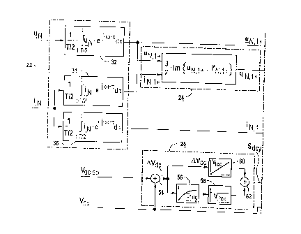
Figure 2 shows, in greatE=r detail, a block switching diagram
of an apparatus for executing the inventive method. This
apparatus has an identification device 22, a computing device
24, an intermediate circuit voltage control circuit 26, a
device 28 for determining complex amplitudes uK,l, and uK,l_ of a
compensator voltage fundamental component positive-phase-
sequence and negative-ph<~se-sequence system space vector uK,l+
and uK,l_ and a space vector formation unit 30. The determined
line voltage and line current space vectors u~, and 1N are
supplied to identification device 22. At the output side, this
identification device 22 is connected with inputs of computing
unit 24 and device 28. Likewise, at the output side computing
unit 24 is connected with an input of device 28, which is, in
addition, connected at the input side with an output of
intermediate circuit voltage control circuit 26. The two
outputs of device 28 are connected with space vector formation
unit 30, to which another intermediate circuit voltage actual
value Vd~ is also connected at the input side. At the output of
9
CA 02300306 2000-02-09
this space vector formation unit 30 there is a transmission
ratio space vector ii, from which the control signals S" for
pulse-controlled converter 4 of compensation device 2 are
generated using pulse width modulator 18.
In this block switching diagram, space vectors are
characterized by an arrow, while complex quantities are
underlined. The index 1 :indicates a fundamental component
quantity, and index + or - identifies the positive-phase-
sequence system or the negative-phase-sequence system. The
index of parallel :>trokea or perpendicular strokes (II or 1)
indicates that these complex amplitudes run in the direction
of, or perpendicular to, the line voltage fundamental
component positive--phase-sequence system space vector a N,1+.
The output quantities of the controller are scalar quantities.
A complex quantity with a superscripted star indicates a
conjugated complex quantity.
Identification device 22 has a computing unit 32, 34 and 36
for each amplitude uN,l+, iN,~+, and iN,l_ to be identified.
Determined line vo7_tage apace vector uN is supplied to
computing unit 32, and determined line current space vector 1N
-,
is supplied to computing units 34 and 36. At the output of
computing unit 32 there is a complex Fourier coefficient u~,,l+,
having ordinal number 1 of the observed oscillation of the
positive-phase-sequence system. At the output of computing
unit 34 and 36, there is likewise a complex Fourier
coefficient iN,l+ and i~,,l_, respectively. Each complex Fourier
coefficient contains information about the magnitude and phase
position of the quantity to be identified, in relation to a
reference space vector (unit space vector). For this reason,
CA 02300306 2000-02-09
in the following these calculated complex Fourier coefficients
urr,~+. irr,l+. and iN,l_ are called amplitudes. These complex Fourier
coefficients are obtained using a discrete complex Fourier
transformation. A block switching diagram of a discrete
complex Fourier transformation is illustrated in the above-
cited conference report. This discrete Fourier transformation
is made up of a complex multiplication with subsequent mean
value formation. In the complex multiplication, the space
vector to be identified .is multiplied by a unit space vector,
and the complex product .is averaged over a period of the space
vector to be identified. With respect to the dynamic response,
here averaging takes place over a half period. For the
identification of this discrete complex Fourier
transformation, the. corresponding equations are indicated in
computing units 32, 34, and 36. At the outputs of this
identification device 22 there are thus available the complex
amplitude uN,l+ of the line voltage fundamental component
positive-phase-sequence system, the complex amplitude iN,l+ of
the line current fundamental component positive-phase-sequence
system, and the complex amplitude iN,l_ of the line current
fundamental component negative-phase-sequence system.
The outputs of ider.,tification device 22, at which complex
amplitudes u~,,l+ and iN,l+ of the fundamental component positive-
phase-sequence system arE: available, are connected with the
inputs of computing' unit 24. The output of identification unit
22, at which complex amp7_itude iN,l_ of the fundamental
component negative-phase-sequence system is available, is
connected with a second input of device 28 for determining
complex amplitudes uK,l+ and uK,l_ of a compensator voltage
fundamental component positive-phase-sequence and negative-
phase-sequence system. From the available fundamental
component positive-phase-sequence system portions uN,l+ and
iN,l+, computing unii~ 24 calculates a positive-phase-sequence
system fundamental component reactive power q~,,l, -- which is
11
CA 02300306 2000-02-09
supplied to a first: input of the downstream device 28 --
according to the following equation:
qN; ~+ _ ( 3 / 2 ) ~ Im { L~_r~, ~+ ' i. *~,, ~+
In order to compensate the fundamental component positive-
phase-sequence syst:em reactive current, this calculated
positive-phase-sequence system fundamental component reactive
power q~,,~+ must be ~zontrolled to zero. For this purpose, device
28 has a first PI controller 38, which is connected at the
input side with the first input of this device 28. At the
output of this PI controller 38 there is a reactive power
manipulated quantity Sqy as a controller output quantity, which
is multiplied with determined complex amplitude u,~,l+ of the
line voltage basic system, using a first multiplication unit
40. At the output of this first multiplier 40, which is
connected with an input of an adder 42, there is a voltage
amplitude uK,l+ii of a compensator voltage fundamental component
positive-phase-sequence system space vector uK,l+, this
amplitude running parallel to amplitude uN,l+ of line voltage
fundamental component positive-phase-sequence system space
vector a N,1+. Using this voltage amplitude uK,l+~ i. with the aid
of matching filter 8 a portion is produced in the current iN
that is perpendicular to the positive-phase-sequence system
line voltage u~,,l+, and in this way positive-phase-sequence
system fundamental component reactive power qN,l+ is controlled
to zero.
A second PI controller 44 is connected downstream from the
second input of device 28, and a current manipulated quantity
Sly is available at the output of this controller as a
12
CA 02300306 2000-02-09
controller output quantity. This scalar current manipulated
quantity Siy is multiplied with negative imaginary unit -j
using a second multiplication unit 46, and in this way the
current manipulated quantity Siy is rotated by -90°. The sign
of imaginary unit j depends on the reference arrow system
used. Since in Figure 1 the load reference arrow system is
used, imaginary unit j is negative. At the output of this
second multiplier ~l6 there is a complex amplitude uK,l_ of a
compensator voltage fundamental component negative-phase-
sequence system space vector uK,l_, with which the fundamental
component negative-phase-sequence system in line current 1N is
controlled to zero.
In addition, this device 28 also has a device 48 with which a
voltage amplitude 1.1 K,l+1 of compensator voltage fundamental
component positive-phase-sequence system space vector uK,l+ is
generated, which runs perpendicular to amplitude u~,,l+ of line
voltage fundamental component positive-phase-sequence system
space vector uN,l+. ,his device 48 has two multipliers 50 and 52
that are switched one after the other. The second input of
multiplier 52 is connected with the output of intermediate
circuit voltage control circuit 26, at whose output there is
an intermediate circuit manipulated quantity Sd~y. The one
input of multiplier 50 is connected with the first output of
identification device 22, a negative imaginary unit -j being
available at the second input thereof. Since according to
Figure 1 the load reference arrow system is used,
multiplication takes place by negative imaginary unit j. Using
this multiplier 50, complex amplitude uN,l+ is rotated by -90°,
and this amplitude is subsequently multiplied by intermediate
13
CA 02300306 2000-02-09
circuit manipulated quantity Say. Voltage amplitude uK,l+1 of
compensator voltage fundamental component positive-phase-
sequence system space vector uK,l+ is then available at the
output of this mult:iplie:r 52, and this amplitude controls a
determined intermediate circuit voltage difference ~Va~ to
zero.
Intermediate circu:_t manipulated quantity Saw is determined
using intermediate circuit voltage control circuit 26. For
this purpose, this control circuit 26 has at the input side a
comparator 54 at whose non-inverting input there is available
an intermediate circuit voltage target value Va~soll and at whose
inverting input there is available a determined intermediate
circuit voltage act:ual v<~lue Va~. At the output of this
comparator 54 there is available an intermediate circuit
voltage difference ~Va~. 'This control deviation ~Va~ is smoothed
using a first-order. delay element 56, before being amplified
using a P-controller 58. This smoothing of the control
deviation ~Va~ is required because, due to the load
symmetrization, int:ermed_Late circuit voltage actual value Va
generally contains an alt=ernating portion having twice the
network frequency, and this alternating portion must not be
amplified by P-cont:roller_ 58. An I-controller 60, connected at
the input side with the output of comparator 54, removes the
remaining control deviat_Lon that would arise given the
exclusive use of a P-cont=roller 58. The controller output
quantities of I- and P-controllers 60 and 58 are superposed,
using an adder 62, to form intermediate circuit manipulated
quantity Sa~Y.
Output-side space vector formation unit 30 has at the input
side two multiplication units 64 and 66 that are each
connected at the output side with a respective input of an
adder 68. At the output aide, this adder 68 is connected with
14
CA 02300306 2000-02-09
a second multiplier 70 whose second input is connected with
the output of a reciprocal formation unit 72, at whose input
there is available a determined intermediate circuit voltage
actual value Vd~. The output of additional multiplier 70, at
which there is available a transmission ratio space vector Li,
_-,
is connected with pulse-width modulator 18 of automatic
control device 10 of pulse-controlled converter 4, said
modulator generating -- dependent on this transmission ratio
space vector ii -- control signals S~ for pulse-controlled
converter 4, so that this pulse-controlled converter 4
generates determined compensator voltage fundamental component
space vector uK,l. Input--side multipliers 64 and 66 of this
space vector format=ion unit 30 are each connected with an
output of device 28, at which there is available a complex
amplitude uK,l+ and uK,l_ of a compensator voltage fundamental
component positive--phase-sequence system and negative-phase-
sequence system space vector a K,1+ and a K,1_, respectively. In
order to form the positive-phase-sequence system and negative-
phase-sequence system space vectors a K,1+ and a K,1_ from these
--,
determined amplitudes uK,l+ and uK,l_, these complex amplitudes
uK,l+ and uK,l_ are multiplied with a unit space vector a+'"t and
e-'"tof the positive-phase-sequence system and negative-phase-
sequence system. The superposition of these compensator
voltage fundamental- component positive-phase-sequence system
and negative-phase--sequence system space vectors a K,1+ and a K,1-
->
yields the compensator voltage space vector uK,l, which the
pulse-controlled converter 4 must generate in order to control
to zero the calculated positive-phase-sequence system
CA 02300306 2000-02-09
fundamental component reactive power qN,l+, the fundamental
component negative--phase-sequence system in the line current
1N, and the intermediate circuit voltage difference ~Vd~~
In this way, a method is obtained for a compensation device 2
having a pulse-controlled converter 4 that has at least one
capacitive memory Ei that is coupled parallel to the network
14, with which a highly dynamic load symmetrization and
reactive power compensat_Lon is achieved. Using this highly
dynamic load symmet:rization and reactive power compensation,
undesirable change; in line voltage that cause flicker are
avoided to the greatest possible extent. That is, with respect
to the fundamental component the load itself appears, from the
point of view of overlay network 14, as a three-phase
symmetrical ohmic resistance.
16