Note: Descriptions are shown in the official language in which they were submitted.
CA 02300919 2000-02-18
WO 99!10853 PCTNS98/17266
1
METER1~1G CIRCUIT
CROSS REFERENCE TO RELATED APPLICATIONS
The present invention is a continuation-in-part of U. S. Patent
Application No. 08/758,248 to Afilani filed on November 27, 1996, the
disclosure in which is incorporated herein by reference and is attached hereto
to as Appendix A. In addition, the present invention is a continuation-in-part
of
U.S. Application No. 08/840,069, to Afilani, filed on April 24, 1997, the
disclosure in which is also incorporated herein by reference and is attached
hereto as Appendix B.
FIELD OF THE INVENTION
The present invention relates to methods and apparatus for locating
various entities by detecting dielectrokinesis response in the entity. In
particular, the present invention relates to a method and apparatus for
2o detecting and metering current indicators of the dielectrokinesis response.
BACKGROUND OF THE INVENTION
Humans, animals, organic objects and other entities generate an
external electric field and gradients thereof which cause polarization, de-
polarization and re-polarization phenomenon in cellular membranes. These
phenomenon result in polarization states which can be detected by a detector
device as described in U.S. Patent Application Nos. 08/758,248 and
08/840,649, attached hereto as Appendices A and B. The background
information with respect to dielectrokinesis effects and how they can be
detected is thoroughly discussed in those applications attached hereto and
incorporated herein by reference and thus, for the sake of brevity, such a
discussion is not repeated here.
CA 02300919 2000-02-18
WO 99/10853 PCT/US98/17266
2
The present invention relates to an improvement to the detector and
metering circuitry associated with the inventions described in those
applications. In particular the circuitry shown in, for example, Figure 5 of
U. S.
Application No. 08/758,248 (Appendix A) includes an antenna 102 upon
which the forces associated with dielectrokinesis effects act. The antenna 102
is connected to an optimal low pass filter F1, which outputs to a current
detection device (in Figure 5 shown as JFETs J1, J2, and J3). After the
current
detection JFETs, the current continues into a current meter, M1, and an
optional piezo buzzer P1. The current detectors (JFETs J1, J2 and J3),
to together with the meter M1 and piezo buzzer P1 are used to detect the
subtle
currents on the antenna 102 which are induced by the dielectrokinesis effects.
Thus, in accordance with the description of Figure 5 of Application No.
08/758,248, 'the operator employs an antenna to sense the dielectrokinesis
effects associated with the presence of an entity to be detected and thereby
15 creates a very low level current in association with that detection. The
low
level current detector in Figure 5 takes the low level current induced on the
antenna 102 and passes it through the low pass filter F 1 and then to the gate
of
the respective JFETs. If the current exceeds the gate threshold of operation
for the respective JFETs, the JFETs open to thereby complete a circuit
2o powered by battery B 1 and including meter M 1 and piezo buzzer P 1. In
this
way, current induced on antenna 102 will control the operation of meters M 1
and piezo buzzer P 1 in order to thereby detect dielectrokinesis effects in
the
vicinity of the antenna 102 and display them (via meter M1 and piezo buzzer
P 1 ) to the operator.
25 The present invention is a circuit which is designed specifically to
improve detection of the low level currents that are induced in the antenna by
the dielectrokinesis effects of an unknown entity existing in the vicinity of
the
antenna. In particular, it is desirable to improve the distance in which the
detector device can be accurately used to detect the unknown entity. That is,
3o in detectors, increasing the distance that the detector device can
unequivocally
CA 02300919 2000-02-18
WO 99/10853 PCT/US98/17266
identify the presence of the entity is desirable. Unfortunately, as the
distance
between the detector and the detector entity increases, the signal strength
received by detector due to the dielectrokinesis effects of the unknown entity
are dramatically reduced and can thereby result in misidentifications of the
presence of the entity. Since the current levels induced on antenna 102 can
already be relatively low (at or below the JFET gating threshold), reductions
in
the current levels (and hence the signal to noise ratio) can have a dramatic
impact on the operational characteristics including the maximum effective
distance of detection.
to In addition, the detector described with respect to Appendix A and B
includes circuitry which is designed to sense the electric field in the
vicinity of
the detector caused by dielectrokinesis effects induced by the presence of the
unknown entity. The detection occurs as a result of the induced current on the
antenna 102 exceeding the gate threshold on the JFETs J1, J2, and J3. Current
~5 levels below the threshold will fail detection. This method can provide low
sensitivity of operation since the operator will receive either a positive
indication (via meter movement and piezo buzzing) if the current threshold is
exceeded or no indication at all if it is not.
SUMMARY OF AN EXAMPLE EMBODIMENT OF THE INVENTION
The present metering circuit operates in conjunction with the antenna,
filtering and detector circuit described in Appendix A and B. By replacing the
JFETs of Figure 5 of Appendix A with the present circuit, the operator can
detect more subtle indications of the presence of an unknown entity.
With the present metering circuit, the operator sets the detection level
to a particular value (preferably a null value) such that changes in the
dielectrokinetic effects are more sensitively detected. Thus, for example, if
30 ambient levels of electric field are 20 micro volts per cm and the change
in field
caused by the dielectrokinesis effect of introducing an unknown entity into
the
CA 02300919 2000-02-18
WO 99/10853 PCT/US98/17266
4
effective range of the antenna 102 causes a +1 micro volt per cm change in
ambient conditions, the change from 20 to 21 on a meter might be
indistinguishable to the JFET gates. In such a case, the meter and piezo
buzzer
would not adequately distinguish between an ambient condition and a changed
condition.
If, however, the current detection circuit "zeros" itself at the ambient
condition, the change from zero (ambient condition) to +1 micro volt per cm
(when the unknown entity is introduced into the effective range of the antenna
102) can be more sensitively identified by the detection circuit and thereby
provide a more obvious identification to the operator of the presence of an
unknown entity.
The present invention thus advantageously provides improved
sensitivity iri detecting the presence of unidentified entities and also
provides
increased distances of effective operation.
BRIEF DESCRIPTION OF THE DRAWIN S
Other advantages and objects of the present invention will be described
in detail with reference to the accompanying drawings, in which:
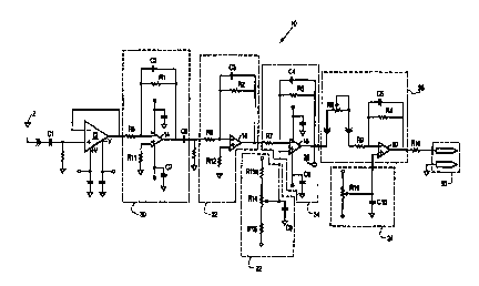
FIGURE 1 is a circuit diagram of an example embodiment of the
present invention.
DETAILED DESCRIPTION OF THE
PERSENTLY PREFERRED EMBODIMENTS
Figure 5 of Appendix A shows a circuit diagram in which an antenna
I 02 detects an electric field in the vicinity of the detector and delivers a
low
3o value current to a current detector circuit The present invention can be
CA 02300919 2000-02-18
WO 99/10853 PCT/US98/17266
substituted into the apparatus described in Appendix A in connection with the
same antenna 102 by substituting the circuit of Figure 1 (attached) for the
current detection circuit of Figure 5 of Appendix A.
In this regard, Figure 1 of the present invention illustrates an example
embodiment of the improved current detector circuit 10. As shown in Figure
1, the circuit 10 is connected to antenna 2 (coinciding with antenna 102 of
Figure 5 of Appendix A). The antenna 2 provides a low level current as
electric fields are brought into effective proximity to it. The current
detector
circuit 10 senses the current provided by antenna 2 and provides an indication
of that current to the operator via meter 50, in accordance with the purposes
described with respect to U. S. Application No. 08/758,248.
The present current sensor 10 includes a series of amplifiers, beginning
.:. ..
with a first operational amplifier 12 connected to a series of amplifier
circuits
30, 32, 34, and 36. Operational amplifier 12 is preferably a low noise, low
~5 frequency precision Op amp that permits very low level input currents (on
the
pico amp level). An example operational amplifier suitable for the present
current detector is marketed by Analog Devices of Norwood, Massachusetts
under the product no. AD645, a data sheet corresponding to which is attached
as Appendix C, which is incorporated herein by reference. Alternative
2o amplifiers can be used provided they have a voltage noise spectral density
curve to operate at a frequency at which the dielectrokinetic effects can be
detected with su~cient sensitivity. For example, for detection of humans by
detection of the dielectokinetic effects of the electrical signals in a human
heart,
an amplifier with a voltage noise spectral density curve to operate around 18
25 Hz or less, and preferably around 10 Hz, will suffice. Other-and different-
operational characteristics may be more appropriate for detection of other
types of entities or for detection of alternative physiological
characteristics of
human entities.
CA 02300919 2000-02-18
WO 99/10853 PCT/US98/17266
6
The frequency of operation for detecting a human depends upon the
beat frequency of the heart. Typically, the beat frequency is around 1-2 Hz.
By Fourier transforming the beat signal, one finds a fundamental frequency at
about 17.5 Hz (hence the ideal operational characteristic of 18 Hz, or less).
Of
course, higher frequencies can be employed by focusing on the higher end
components of the Fourier signal up to any frequency level for which the
signal
to noise ratio remains low enough to extrapolate a usable signal. The
inventors
have found that with present technology such higher and Fourier components
can be employed up to about 50 Hz in Europe and 60 Hz in the U.S. before
to background noise overcomes the Fourier component signals.
The inverting input of the operational amplifier 12 receives a feedback
signal from the output of OP amp 12. The non-inverting input of the
operational amplifier 12 receives the antenna signal via series capacitor C 1.
C I
may be chosen based on the specific design constraints of the system used, hut
15 may preferably be a metal film capacitor of, for example, 0.47N,F.
The output of the operational amplifier 12 is then feed into the
inverting input of amplifier 14 within first amplifier stage 30 via the
resistor R5.
Each of the amplifier stages 30, 32, 34, and 36 includes such a resistor {R5,
R6, R7, and R8+R9) at the inverting input. In addition, the output of each of
2o the amplifiers 14, 16, 18, and 20, of respectively, amplifier stages 30,
32, 34,
and 36 is fed back to the inverting input of the respective amplifier via the
parallel combination of corresponding resistors and capacitors R1, R2, R3, R4,
and C2, C3, C4, and C5. Also at the output of amplifier 14 is coupling
capacitor C6 which may be a 2.2. ~F ceramic capacitor connected in series
25 between the amplifier 14 and the second amplifier stage 32.
The non-inverting inputs of amplifiers 14 and 16 are tied to ground via
resistors R11 and R12. For the non-inverting inputs of amplifiers 18 and 20 of
amplifier stages 34 and 36, respectively, automatic nulling adjustments are
provided. In particular, at the third amplifier stage 34, the non-inverting
input
30 of amplifier 18 is connected to variable resistor R14, which is connected
in
CA 02300919 2000-02-18
WO 99/10853 PCT/US98/17266
7
series to positive voltage (for example, + 9 volts) through resistor R13 and
is
connected to minus voltage (for example, - 9 volts) through resistor R15. The
variable resistor R14 makes up a part of the zero offset adjustment circuit
22,
which is connected to the non-inverting input of the amplifier 18.
Zero offset adjustment circuit 22 is provided to permit the operator to
adjust the gain of the third stage to accommodate drift that may exist in the
high gain amplifier stages. As an example embodiment of the zero adjust
circuit 22, resistor R3 may have a value of 100K ohms, resistor R15 may have
a value of 1 OOK ohms and resistor R 14 may have a value of SK ohms. Further,
1o capacitor C9 may have a value of Ø1 ~,~F and may be a metal film
capacitor.
The fourth amplifier stage 36 includes amplifier 20 and input resistors
R8 in series with R9. Resistor R8 is variable and may have a value of 250K
ohms, while resistor R9 is fixed at a value of 220 K ohms. Resistor R8 is a
potentiometer which provides a sensitivity adjustment for the operator. In
addition, adjustment circuit 24 is provided into the non-inverting input of
amplifier 20 to provide a center adjustment for the meter being used. This
allows the operator to determine whether the presence of an unknown entity
causes the metering circuit to build capacitance or to draw capacitance.
Center
adjustment circuit 24 includes variable resistor R16 connected between
2o positive and negative voltage. It may be a 50 K ohm resistor connected in
parallel with capacitor C 10 which may be a 0.1 microfarad metal film
capacitor. Ideally, R16 is adjusted for half scale (i.e., centered on the
meter)
when no input signal is present.
The output of the fourth amplifier stage 36 is provided to a resistor
R10 which may be 47 K ohms, but will be adjusted depending upon the meter
used. The output of the resistor R10 is provided to the meter 50 which will
identify the presence of current at the antenna 2 to the operator, as
amplified
by the various amplifier stages discussed previously.
In operation, a very small current is detected in arnenna 2 whenever the
3o dielectrokinetic effects cause a change in electric field compared to
ambient
CA 02300919 2000-02-18
WO 99/10853 PCT/US98/17266
8
conditions. This current may be in the order of picoamps and is provided
through blocking capacitor C 1 to the non-inverting input of amplifier 12.
This
amplifier is frequency clipped at 10 Hz which is a preferred frequency at
which
tests show that the subtle dielectrokinesis effects of the presence of an
unidentified entity are seen and coupling between the unidentified entity and
the detector is maximized. The amplifier 12 increases the signal strength and
provides the output to the four amplifier stages 30, 32, 34, and 36. These
amplifier stages further boost the signal value such that the meter 50 at the
output of the current detector circuit 10 can identify to a high degree of
clarity
io the presence of an unidentified entity, even at larger distances such as,
for
example, 20 meters or more.
The circuit 10 will float to ambient electric field conditions such that,
after, for example 2 to 3 seconds, the circuit nulls itself at the ambient
condition. Thereafter, changes in the electric field caused by the
is dielectrokinetic effects of introducing another entity in the vicinity of
the
antenna 2 will be registered by the metering circuit. In this way, any changes
to the ambient condition can be detected with greater sensitivity directly on
the
meter being used, as discussed above.
The present invention is not limited to the precise circuit shown in
2o Figure 1, but may employ other circuit designs which are low pass and keyed
off of a device having a voltage noise spectrai density curve to operate
around
50 Hz or less, and preferably around 10-18 Hz. This allows the circuit IO to
sense a charge on the antenna 2 and use the charge to apply a series of gains
for detection by a meter or other suitable device.
25 The present invention has many uses and is not necessarily limited to
any particular use. The inventors have found that the antenna detector and
metering circuit can be used to detect the presence of hidden entities,
including
humans, animals, polymers, controlled substances, etc. Further applications
include the detection of movement (motion detectors) in a defined
30 environment. For example, when an entity is perfectly still within a room,
the
CA 02300919 2000-02-18
WO 99/10853 PCT/US98/17266
9
present circuit will first detect the entity, then (after a few seconds) null
itself
to the ambient condition. Thereafter, if the entity moves, the meter will
register changes in the dielectrolcinetic effect in the room caused by the
change
in physical orientation of the human's heart relative to the detecting antenna
2
(which in turn changes the electric field sensed by the antenna 2).
Another application of the invention is within the medical diagnostic
field. In particular, the invention can be used to numerically characterize
the
electric field associated with a human heart muscle and the conductive nerves.
This permits the operator to view these electric field characteristics against
a
io norm to provide an indication of health of the heart. One possible
characteristic (of potentially many different characteristics) that can be
detected is the heart rate variability and the synchronization between the
sympathetic and parasympathetic rhythms. In this regard, the present invention
is more sensitive in detecting heart condition than, for example, prior art
ECG
15 tests.
A fi~rther alternative use of the invention is operation in an autonomous
mode, without the presence of a "reference entity" (such as a human operator)
in contact with the ground plane GP1, as shown in Figure 5 of Appendix A and
described at page 12 of Appendix A. The inventors have found that, by
2o choosing the proper operating characteristics of the amplifier 12 (as
described
above and in the example of Appendix C), the detection and metering circuits
will operate without a reference entity in physical connection with the ground
plane. This permits the device to operate as a stand-alone device, without the
need for a physically present operator.
25 While the invention has been described in connection with what is
presently considered to be the most practical and preferred embodiments, it is
to be understood that the invention is not to be limited to the disclosed
embodiments, but on the contrary, is intended to cover various modifications
and equivalent arrangements included within the spirit and scope of the
3o appended claims.