Note: Descriptions are shown in the official language in which they were submitted.
CA 02301440 2000-03-20
METHOD AND SYSTEM FOR CONFIGURING AN AIR INTERFACE IN A
MODEM
FIELD OF THE INVENTION
The present invention relates to a method and system for data transmission in
a
modem. In particular, the present invention relates to a method and system for
configuring an
air interface for data transmission in a modem according to multiple
standards.
BACKGROUND OF THE INVENTION
Generally, modems have been designed to work with one of many existing
standards. For example, while there are many air interface, or radio link,
standards, most current
modems are designed to operate with only one of them. Even within a particular
standard, uplink
and downlink formats are very different, and require separately designed air
interface processors.
Clearly, this results in increased costs for both design and hardware when a
new standard is
implemented, and precludes using a modem designed to work with one standard
from being
reconfigured to work with a different standard.
It is therefore desirable to provide an air interface processor that can be
configured for more than one standard, or data format.
SUMMARY OF THE INVENTION
It is an object of the present invention to provide a method and system that
obviates or mitigates at least one disadvantage of the prior art. It is a
particular object of the
present invention to provide a method and system for configuring an air
interface in a modem
for multiple data and transmission standards and formats.
In a first aspect, the present invention provides an air interface processor
for a
modem, comprising:
an event handler for scheduling the processing of data transmission and
reception in the
modem;
a microsequencer receiving instructions from the event handler and determining
commands to send to a frame formatter in the modem.
-1-
CA 02301440 2000-03-20
According to a further aspect of the present invention, there is provided a
method for processing data, comprising the steps of:
(i) scheduling the processing of data transmission and reception;
(ii) transmitting the schedule to a microsequencer;
(iii) sending commands to a frame formatter to build a frame of data in
accordance
with the schedule.
BRIEF DESCRIPTION OF THE DRAWINGS
Preferred embodiments of the present invention will now be described, by way
of example only, with reference to the attached Figures, wherein:
Figure 1 is a block diagram of a modem incorporating an air interface
processor
according to the present invention;
Figure 2 is a block diagram of an air interface processor according to the
present
invention;
Figure 3 is a chart of event handler instruction sets according to the present
invention;
Figure 4 is a chart of general purpose instructions according to the present
invention;
Figure 5 is a chart of event handler ALU opcodes according to the present
invention;
Figure 6 is a chart of event handler branch conditions according to the
present
invention;
Figure 7 is a chart of register access instructions according to the present
invention;
Figure 8 is a chart of data scheduling instructions according to the present
invention;
Figure 9 is a chart of burst descriptor instructions according to the present
invention;
Figure 10 is a chart of a modulator burst information field format according
to the
present invention;
Figure 11 is a chart of a demodulator burst information field format according
to
-2-
CA 02301440 2000-03-20
the present invention;
Figure 12 is a chart of a processor wait instruction according to the present
invention;
Figure 13 is a chart of a microsequencer instruction set according to the
present
invention;
Figure 14 is a chart of a microsequencer memory format according to the
present
invention;
Figure 15 is a block diagram of a configuration of condition codes and forks
according to the present invention; and
Figure 16 is an example of fork values according to the present invention;
DETAILED DESCRIPTION OF THE INVENTION
A modem incorporating an air interface processors (AIPs) in the modulator and
demodulator, respectively, is shown in Fig. 1. Both the Modulator and the
Demodulator have
special-purpose processors that are designed with the intention of allowing
the Modem to meet
any air interface standard. However, it is impossible to predict whether all
forthcoming LMDS
and SatCom systems can be handled. For any systems which cannot be handled
directly, there
will be a provision to bypass internal FEC generation/correction and process a
raw bit stream.
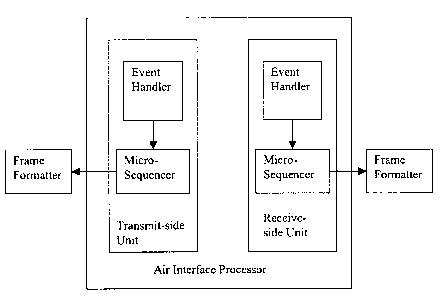
The Air Interface Processor, is generally shown in Fig. 2, and is divided into
a
transmit-side and receive-side unit. Each Processor Unit consists of an Event
Handler and a
Microsequencer. The Event Handler provides an abstraction of the Burst
Frequency Time Plan;
the Microsequencer controls how data is formatted by the ModulatorlDemodulator
circuitry.
The configuration of the Microsequencer is intended to be static during the
course
of operation (though this is not a necessary condition). The Event Handler
configuration is static
for continuous mode operation, and dynamic for burst mode to accommodate
varying Burst-
Frequency Time Plans.
The primary purpose of the Event Handler is to schedule the processing of
burst
data transmission/arnval in the Modem. (Continuous data is treated as a
special subset of burst
data.) In addition to being able to initiate sending/receiving bursts of data,
the Event Handler has
the ability to perform various ALU operations, and to perform conditional or
unconditional
branches. The ALU and branch operations are performed simultaneously, which
allows for
-3-
CA 02301440 2000-03-20
greater code density than would otherwise be possible.
The instruction set is divided into general purpose and modem control
instructions. There are 8 16-bit read/write registers, and 8 16-bit read-only
registers. All
instructions occupy one 48-bit word in memory. The instruction set summary is
shown in Fig.
3. The Event Handler memory is a single-port, synchronous, 1K * 48 RAM.
General-purpose instructions (bits 47:46=00), as shown in Fig. 4, are
comprised
of an ALU instruction and a two-way branch instruction. The ALU instructions
are reminiscent
of the ARM RISC processor, in that the second operand always passes through a
programmable
barrel shifter before being applied to the ALU.
For each operation, the ALU computes a new result and the flags associated
with that result
(Negative, Z=zero, C=carry, V=overflow). The results of the ALU operation are
stored in the
destination register only if the 'W' flag is asserted for that instruction.
The ALU flags are
updated only if the 'S' flag is asserted.
The results of the ALU operation are written to a destination register (Rd).
The
destination register may be any of the 8 read/write registers (RO-R7). Operand
1 (Rn) is always
a register, and may be any of the 16 registers. Operand 2 is either an
immediate value (I=1) or
a register value (I~), and is passed through a programmable barrel shifter to
yield a 16-bit result.
In general, each ALU instruction performs the following operation:
result = fn(Rn, shift(op2))
Rd <= result if w else no change
{N,z,C,v} <= flags(result) if s else no change
The operations supported are shown in Fig. S.
The branch component of the instruction allows a conditional branch to happen
based on the result of the previous ALU instruction. Each branch instruction
has an address
offset to jump to in the case the condition passes, and a separate address
offset to jump to in the
case the condition fails. This mechanism only allows for relative branches.
The branch codes supported are shown in Fig. 6.
Register Access instructions (bits 47:46=O1 ), as shown in Fig. 7, are
provided to
allow reading or writing arbitrary registers within the Modem. The Modulator
Air Interface
Processor can only control registers within the Modulator, and the Demodulator
Air Interface
Processor can only control registers within the Demodulator. This facility is
used to
-4-
CA 02301440 2000-03-20
enable/disable internal ASIC blocks, and to control external devices that need
to be manipulated
on a real-time basis, such as RF frequency select for MF-TDMA systems. It is
not intended for
static configuration, which is better handled via the processor interface
(although it can be
performed here as well).
Rhi provides the top 16 bits of the 24 bit address. Rlo (bit 44=0) or ilnm-to
(bit
44=1) provides the bottom 8 bits. For a write operation (bit 45=0), the 32 bit
data is contained
directly in the lower bits of the instruction. For a read operation (bit 45=1
), the bottom 3 bits
encode the number of the destination register. The register access occurs over
the internal HCPU
bus.
Data Scheduling instructions (bit 47=1), as shown in Fig. 8, are the means by
which bursts of data are transmitted or received by the Modem. Each of these
instructions is an
entry that maps time indices to actions. Time indices are specified in clock
ticks relative to the
start of a super-frame. Time index 0 is determined via the PCR algorithm (PCR
offset). Actions
are pointers to microcode instruction sequences. With this scheme, it is not
necessary to count
frames or even timeslots, only superframes.
For the execute phase of a data scheduling instruction, the Event Handler will
wait
until the current time (time index relative to super-frame start) is
approximately equal to the
trigger time. (It can only wait for the times to be approximately equal
because the Event Handler
runs off the byte clock, whereas the current time is a counter that runs off
the sample clock.)
When the trigger time is reached, a start command is sent to the
Microsequencer, which will
begin running at the address specified in "microsequencer address".
A time offset of 32'hFFFF FFFF is a special code indicating that this event is
to
be processed immediately. The microsequencer address 0 is a special code
indicating that the
start command should not be sent.
the trigger flag is set, the time offset in the current event is passed to the
Preamble
Insert module in the Modulator, or Direct Sampling module in the Demodulator.
Bursts can be conditional on the availability of data in a certain queue. In
this case, the 'D' flag
must be set to 1, and 'Q' must be set to the number of the data queue which
must contain data
(0 ~ DATA1, 1 ~ DATA2, etc).
For burst mode applications, the AIP provides a special BURST instruction, as
shown in Fig. 9, which is used to specify special information related to the
following burst of
-S-
CA 02301440 2000-03-20
data.
The contents of the burst info field are different for the modulator and
demodulator. For the modulator, as shown in Fig. 10, this field is used to
select which preamble
is to be used for the following burst (PS). Up to four preambles may be
defined. For MF-TDMA
applications, the burst info field contains frequency information that is used
to reprogram the
DDS or Fractional-N counter.
For the demodulator, as shown in Fig. 11, the burst info field is used to
select the
expected preamble for the incoming burst (PS). Up to four preambles may be
defined. It also
contains the length of the expected burst. The SB7016 tags all incoming bursts
with an arbitrary
user ID, which the MAC layer software can use to correlate received bursts
with expected bursts
in the BFTP. The user ID is specified in the burst info field.
Fig. 12 shows a typical processor wait instruction.
The Microsequencer is responsible for sending commands to the Frame Formatter.
On the Modulator, this builds up a frame of data on a byte-by-byte basis.
The core of the Microsequencer design is based on a modified version of the
AMD2910 micro-program sequencer. The original 2910 is a 12 bit sequencer with
a 32 word
stack, and is capable of conditional branching, subroutine calls, and looping.
The
microsequencer in the Air Interface Processor is a 10 bit sequencer, but adds
some powerful
instructions, as shown in Fig. 13, to perform mufti-way conditional branching,
among other
things.
The number of microcode sequences is limited only by the available Sequence
RAM (SeqRAM) available. The SeqRAM is a single-port synchronous 1K * 32 RAM.
The Microcode Sequencer has a program counter (PC), which is initially set by
the Event Handler. When it is instructed to start by the Event Handler, it
shall begin executing
the instructions in SeqRAM at the specified address, until such time as a JZ
(jump-to-zero)
instruction is found.
The memory format for the modulator microsequencer is shown in Fig. 14.
The EMIT field is used as an argument to the OPCODE field, and is used for
branch addresses or to load the internal counter. The SR field (Scrambler
reset) can be used to
reset the Scrambler at any time.
The FORK instruction, which is an addition to basic 2910 instruction set, uses
the
-6-
CA 02301440 2000-03-20
value formed by the fork cc(3:0) vector as the basis for a 16-way branch. For
example, if the
value of fork cc is 12, the microsequencer will advance its program counter by
12.
The fork cc value is updated every clock cycle based on the configuration
circuitry shown in Fig. 15. Each bit in fork cc is derived from a programmable
look-up table.
A S-bit value is used as the index to this look-up table.
3 ,. i y~~
i' ~.. 6 His ~. >T4~ 5~1, r ~ _~'~~~h~~~~. r, ~~~
xd,. s~ljyi,i~ "" ~$~~',
t5'~~~ >
' ~r5.
~<..bi!.
,..
3
FORK LUT pcr end of counter counter r0
0 insert message < threshold=_
in
_ ueue 1 threshold
FORK LIJT pcr end of counter counter rl
1 insert message < threshold==
in
_ ueue 2 threshold
FORK Llff pcr end of counter counter r2
2 insert message < threshold==
in
_ ueue 3 threshold
FORK Llff pcr end of counter counter r3
3 insert message < threshold==
In
_ ueue 4 threshold
Table 1: FORK LUT Indices
Programming the FORK instruction is a rather convoluted process, as it
involves
three layers of indirection. The FORK instruction is essentially a "case"
statement. The idea is
to generate a 4- -bit value (fork cc) to create an offset of 0 to 15. Each bit
of fork cc is derived
from the corresponding FORK LUT. Each FORK LUT is indexed by the 5-bit number
formed
by the concatenation of the conditions shown in Table 1. The conditions r0,
rl, r2, and r3 are bits
from the R7 register in the Event Handler. The R7 Bit Select register can be
used to select
among the lower 8 bits of the R7 register. Refer to Figure 15 for more
details.
For example, suppose we wanted fork cc(0) to evaluate as true whenever
insert_pcr and counter-=threshold are both true. This condition can be
expressed as lxxlx,
which means that bits 4 and 1 must be 1, and the other bits are don't cares.
In this case, we
would program the bits in the LUT that match lxxlx with 1, as shown in Fig.
16, and the others
with 0. The value generated is 32'hCCCC 0000.
The condition codes (CCSEL) for conditional branches (for example, CJV) in the
Microsequencer are hard-coded as follows:
CA 02301440 2000-03-20
t ~a ~t
.r.,~ .. W , 8..,..">
t
n: y" = a", ,
~ 7~. 5 a , 5' .
~~ ~~'0~2.5 n" 9s % s 3
. ". 1 >_ 'R~,a.rc.2'.
Y.j'_ , ". .t-,
!~s , ~
- a' s ~ ~ . ~ m
91' , t. ' .s
J , a.
,(, ~ : '....~,
, 90... _. S n...r:,
'.u ~t .".7.,.
, n., .. ,.~.r
)..?.~. .~ ~l
'
".. ~3 w.,.vt.
x. ~r,'.,
f g 'ii z~''e.
4 ~ ~ , L x, t7,~
~~'~'~y.,. , x
o n.<.e~:'.Jt,.i~..J..
~~o-,'.~., i. Mx..ar
t'~, ~._..7...
~ 5~3~".~..~"
, .. nip~,t ~~
~~ if la~~ard,
.$~~"iS.,.~..r,
~. .. ~.c._ ,~
~ k ~.~
0 alwa s false
_ _
1 counter= 0 .
2 counter == threshold
3 counter < threshold
4 counter <= threshold
insert cr == 1
6 end of messa a
in ueue 1
7 end of messa a
in ueue 2
8 end of messy a
in ueue 3
9 end of messy a
in ueue 4
insert cr ==1 AND ueue 1
end of messy a
in
11 insert cr ==1 AND ueue 2
end of messy a
in
12 insert cr ==1 AND ueue 3
end of messy a
in
13 insert cr ==1 AND ueue 4
end of messy a
in
14 value of R7 bit
9
value of R7 bit
8
Register R7 in the Modulator Event Handler can be used to control the
Microsequencer to some degree. Bits 8 and 9 of the R7 register are used to
generate condition
codes 14 and 15. Bits 0 to 7 of the R7 register, in conjunction with the
static R7 Bit Select
register, can be used as inputs to the FORK LUT.
The read-only Event Handler registers for the Modulator contain the following
values:
PI! ~ i i Iq6l~',i I i I A ii I~ ~~~I'~i~, I '~~w
' ~~~?''~i I
t ~lal ~ ~~, , ueue 1
rc es remaininin
R8 messy
a
R9 es remaininfn ueue 2
messy
a
R10 B es in ueue 3
remaininmessy
a
Rll B es in ueue 4
remaininmanna
a
R12 Conditioninter
Code
R13 Event
Handler
Pr
ram
Counter
R14 32'h0000
0000
R15 32'hFFFF
FFFF
The definition of FFCMD (Frame Formatter command) is shown in Table 2. This
instruction set is used to generate frames to be fed into the modulator Frame
Formatter. As data
or control words are inserted, they can be flagged with an attribute
indicating whether or not they
should be scrambled, and which outer code is to be used (ie. Reed-Solomon,
CRC, or neither).
If the SB bit is asserted in the Microsequencer instruction, the Scrambler is
bypassed. The value
in the OC field is used to select which outer coding scheme is to be used (0-
3).
The Frame Formatter is also able to insert register values from the Event
Handler
into the data stream. This mechanism allows the generated data stream to be
more dynamic than
would otherwise be possible. When the Event Handler issues a start command to
the
Microsequencer, the contents of RO to R7 are passed through a programmable
barrel shifter and
_g_
CA 02301440 2000-03-20
stored as inputs to the Frarne Formatter.
i F'
ai;'i~ ~:sx> y a,pry-s:
,S.M "3. -r . ~ t w_q ~P ..o.:.y..
B..~s~s.: ,!~ ", fF N , 1-,., ~ rv '
'f,. , ~,i ~~ ~~~v
o,:iH / t ,
s ;...~ .~ 8.. : . ~.,~., r i , i' r ~ "J
n.~.,~ a_.~.i...: .~.. .. ~. f . t .. I ~'~.'~ 1.
: ~ ,. ,~ ~ ~;. ,. ;n , 6 a ~,. z 1,
1~ , x, , s ,5.. ~,; ,: n,~~~S ~ d,
~, n~~CrHnra~,t..~'~lon.~~ ~1.-~a.~~s,o...~.~.*i$~...~, ,: ~.
i~~~y. ~f~~~~i t a;~.
0 no __ NOP
1 - 16 Insert Control Word 1 - 16 CW1 - CW16
17 - 24 Insert Shifted Re inter 0 - 7 RO - R7
25 Insert Ori final PCR PCRO
26 Insert Current PCR PCR
27 Insert Data from ueue 1 DATAl
28 Insert Data from ueue 2 DATA2
29 Insert Data from ueue 3 DATA3
30 Insert Data from ueue 4 DATA4
31 Flush FLUSH
Table 2: Modulator Command Set for Frame Formatter
The most common use of the barrel shifter is to align an 8-bit value in one of
the
registers to the upper 8 bits of the 16-bit register value (inputs to the
Frame Formatter must be
MSB-aligned). The barrel shifter is configured as follows:
Each Rx shift field is defined as follows:
2b00 = LSL (Rn, shift_by) shift_by
2b01 = LSR (Rn, shift-by)
2b10 = ASR (Rn, shift-by)
2b11 = ROL (Rn, shiftby)
A simple microcode sequence to generate an MPEG frame for a base station could
be programmed in the following manner. This sequence indicates that all bytes
except for the
initial sync should be scrambled (".S")
MPEG_FRAME:
CONT Cwl.OCl # 1 byte, typically 47h
CONT CW2.s.OC1 # 1 byte
CONT CW3.S.oC1 # 1 byte
CDNT Cw4.5.OC1 # 1 byte
LDCT 182 DATA2.s.oC1 # send data, from queue 2, load counter
loop: RPCT loop DATA2.S.oC1 # continue pulling data from queue 2
# until counter reaches zero; total = 184
7z FLUSH # indicates end of burst; soft reset
The device can act as a simple ATM segmentation engine by setting the control
-9-
CA 02301440 2000-03-20
word to a 5-byte ATM header. Up to 16 simultaneous ATM connections can be
handled in this
manner (one per Control Word).
CONT C1N1.5.OC1 # cW1 = 5-bytes = { vPI/vcI=(a,b) }
LDCT 2 NOP # 4 NODS because Cwl is S bytes
lOOpl: RPCT lOOpl NOP
LDCZ 46 DATA1.5.OC1 # send 48 bytes from queue 1
lOOp2: RPGT lOOp2 DATA1.5.OC1
72 FLUSH
The above-described embodiments of the invention are intended to be examples
of the present invention. Alterations, modifications and variations may be
effected the particular
embodiments by those of skill in the art, without departing from the scope of
the invention which
is defined solely by the claims appended hereto.
-10-