Note: Descriptions are shown in the official language in which they were submitted.
CA 02301477 2000-03-21
METHOD AND APPARATUS FOR ADDING AND REMOVING
COMPONENTS WITHOUT POWERING DOWN COMPUTER
SYSTEM
FIELD OF THE INVENTION
This invention generally relates to computer systems such as
personal computers, workstations and servers, and more particularly to
computer systems that permit the addition or removal of components
without powering down.
BACKGROUND OF THE INVENTION
Computer servers have become essential in business environments,
providing mission-critical applications, such as business databases, e-mail,
and company-wide local area networks. Loss of access to such
applications for even short periods of time can have enormous impact on
business operations. To achieve high availability, system providers often
take special measures such as incorporating component redundancy, e.g.,
redundant power supplies, redundant network interface cards (NICs), or
redundant arrays of independent disks (RAID) storage systems.
Significant attention has recently been focused on providing high
availability for the Input/output (I/O) subsystem of computer servers. The
PCI local bus (or simply, the "PCI bus") is widely used for I/O subsystems.
The PCI bus is an industry-standard bus for connecting peripherals and
other components in accordance with the PCI Local Bus Specifications,
Revision 2.1, June 1, 1995, (the "PCI Spec"), which is available from the
PCI Special Interest Group, Portland, Oregon, USA, and incorporated
herein by reference.
Over time, peripherals may have to be repaired or upgraded with
additional functionality. Historically, this often required the computer
server to be powered down while the repair or upgrade was effected. The
-1-
a CA 02301477 2000-03-21
c
PCI Spec in its basic form did not provide for components to be connected
to the PCI bus while the computer server is powered up. Such hot-plug
capability was added to PCI buses conforming to the PCI Hot-Plug
Specification, Revision 1.0, October 6, 1997 (the "PCI Hot-Plug Spec"),
which is available from the PCI Special Interest Group, Portland, Oregon,
USA, and incorporated herein by reference.
Accordingly, the PCI Hot-Plug Spec is an enhancement to the PCI
Spec that allows adapter cards to be inserted into or removed from PCI bus
slots at any time, even while the system is powered on, so as to provide
high system availability and serviceability. An adapter card is typically a
circuit board that includes chips and other electronic components
electrically interconnected to add functions or resources to a computer
server or other computer system into which it is installed. PCI adapter
cards are designed in accordance with the PCI Spec to be plugged into a
PCI-compliant slot of a PCI bus. Adapter cards can take the form of
expansion cards that, for example, add memory, disk-drive controllers,
video support, parallel and serial ports, internal modems, and/or network
interfaces ("NICs").
Generally speaking, hot-plugging is a process of inserting or
removing an adapter card from a computer server or other computer system
without stopping software running on the system or powering down the
system as a whole, though running of certain software may be stopped, or
certain hardware powered down. To achieve hot-plugging, the I/O
subsystem of a server or other computer system is provided with a hot plug
controller for controlling hot plugging operations, and devices (e.g.,
electronic switches) for isolating slots from bus signals by selectively
decoupling the slots from the PCI bus during card insertion and removal.
Typically, hot plug administrative software is provided as well for
coordinating hot-plugging activities and interfacing with the server's
-2-
CA 02301477 2000-03-21
v
operating system (O/S), and, through a graphical user interface (gui), with
a technician at a console. Each adapter card typically has an adapter driver,
and the hot-plug controller has a hot plug system driver that interfaces
through the server's operating system with the hot plug administrative
software.
While computer systems equipped with PCI buses having hot-
plugging capability are generally suitable for their intended purposes, it
would be desired to improve their capability so as to overcome certain
drawbacks. For example, following hot plug insertion, malfunctioning of a
newly inserted adapter card can cause serious problems, such as lost or
corrupted data or hanging of the bus protocol so as to prevent completion
of a bus transaction. For example, if an adapter card's connection were to
break at a PCI control signal, such as FRAME#, the card might not respond
when addressed by the server's CPU, and critical data may be lost. In
extreme cases, malfunction of the newly installed adapter card can cause a
system crash. It may even prevent the system from booting up again.
Needless to say, such problems can interfere with diagnosis and repair of
the problem adapter card. While this is true of servers regardless of
whether they are hot plugging capable, in servers equipped with hot plug
capability, this drawback undermines the advantages of high availability
and serviceability otherwise attainable by hot plug technology.
Moreover, existing systems can have problems when a newly
inserted adapter card comes on-line, i.e., is electrically connected to (and
no longer isolated from) the PCI bus for bus signaling purposes. The
problems in this instance are associated with the sudden change in the
electrical characteristics of the bus, which can result in "glitches" (i.e.,
electrical anomalies) on the bus. These can potentially cause the newly
inserted adapter card (or another device then on the bus) to misinterpret the
bus signal levels and operate erroneously. This problem is exacerbated by
-3-
CA 02301477 2000-03-21
increased loading of devices on the bus, as occurs with the addition of a hot
plug controller and adapter cards. Signals on the bus tend to degrade as
they propagate from device to device on the bus; with additional devices on
the bus, the signals degrade that much more. Such glitches and signal
degradation may not present a significant problem, however, if the PCI bus
is allowed to run at a slow enough speed for adequate signal capture under
existing load conditions. For this reason, PCI buses equipped for hot
plugging are generally operated today at a nominal speed of 33 MHz (i.e.,
in a range up to 33 1/3 MHz), as defined in the PCI Spec. However, PCI
buses are allowed to operate also at the higher nominal speed of 66 MHz
(i.e., in a range between 33 1/3 MHz and 66 2/3 MHz), as defined in the
PCI Spec. It would be desirable to run PCI buses equipped with hot
plugging capability at the higher speed.
SUMMARY OF THE INVENTION
The invention resides in a hot plugging system having a first
mechanism for selectively connecting, responsive to a first control signal,
each of a plurality of slots with a primary bus, e.g., a PCI bus connected to
a system bus of a computer system; and a second mechanism for
connecting, responsive to a second control signal, at least one of the slots
with a secondary bus, e.g., a dedicated PCI bus, or other connection
interface, used for testing purposes during hot-plug insertion of an adapter
card received in the at least one slot. The system can also have a controller
for applying the first and second control signals to the slots so as to switch
the connection of the at least one slot to the primary bus from the
secondary bus after testing validates operation of the adapter card(s).
In accordance with another aspect of the invention, the hot plug
controller makes the connection of the at least one slot to the primary bus
in response to a BUS IDLE signal from the host bridge that indicates when
-4-
CA 02301477 2000-03-21
the PCI bus is idle. The BUS IDLE signal can be generated from the
FRAME and IRDY signals for the primary bus by combinational logic in
the host bridge. In this way, the hot plug controller need not be connected
to and load the shared lines, e.g., the FRAME and IRDY lines, of that bus.
Accordingly, the primary bus may be operated, depending on conditions, at
the higher permitted speeds. The hot plug controller according to this
aspect of the invention is connected to the host bridge by a pair of
REQUEST and GRANT lines so as to be able to gain control of the
primary PCI bus, and by a BUS IDLE signal line to indicate when the hot
plug controller can connect newly inserted adapter cards to the primary bus
and thereby bring them on line for normal operation of the computer
system.
BRIEF DESCRIPTION OF THE DRAWINGS
The above and further advantages of the invention may be better
understood by referring to the following description in conjunction with the
accompanying drawings in which:
Figure 1 is a block diagram of an illustrative architecture of a
computer system in accordance with the prior art;
Figure 2 is a block diagram of a conventional hot plug arrangement
for the computer system of Figure 1;
Figure 3 is a block diagram of an improved hot plug arrangement
for the computer system of Figure 1 in accordance with an embodiment of
the invention;
Figure 4 is a block diagram of an embodiment of the hot plug
controller of Figure3;
Figure SA is a block diagram of an embodiment of the isolation
mechanism of Figure 3;
-5-
' CA 02301477 2000-03-21
Figure SB is a schematic diagram of an implementation of the
isolation mechanism of Figure SA;
Figure 6 is an illustrative state transition diagram for operation of
the isolation mechanism of Figure SA;
Figure 7A is a block diagram of an improved hot plug arrangement
for the computer system of Figure 1 in accordance with an alternative
JTAG-based embodiment of the invention;
Figure 7B is a block diagram of an embodiment of the hot plug
controller of Figure 7A;
Figure 7C is a block diagram of an embodiment of the isolation
mechanism of Figure 7A;
Figure 8A is a block diagram of an improved hot plug arrangement
for the computer system of Figure 1 in accordance with yet another
alternative embodiment of the invention; and
1 S Figure 8B is a block diagram of an embodiment of the hot plug
controller of Figure 8A.
DETAILED DESCRIPTION OF THE PREFERRED EMBODIMENT
Figure 1 illustrates a conventional system architecture for an
exemplary computer system 100 with which the disclosed invention can be
implemented. The computer system of Figure 1 is discussed only for
descriptive purposes, and its specific layout and design should not be
considered a limitation of the invention. Although the description below
may refer to terms commonly used in describing particular computer
systems, the described concepts apply equally to other computer systems,
including systems having architectures that are dissimilar to that shown in
Figure 1.
The computer system100 includes a central processing unit (CPU)
105, which may include a conventional microprocessor, random access
-6-
CA 02301477 2000-03-21
memory (RAM) 110 for temporary storage of information, and read only
memory (ROM) 115 for permanent storage of information. A memory
controller 120 is provided for controlling system RAM 110. A bus
controller 125 is provided for controlling bus 130, and an interrupt
controller 135 is used for receiving and processing various interrupt signals
from the other system components.
Mass storage may be provided by diskette 142, CD-ROM 147, or
hard disk 152. Data and software may be exchanged with computer system
100 via removable media, such as diskette 142 and CD-ROM 147.
Diskette 142 is insertable into diskette drive 141, which is connected to bus
130 by controller 140. Similarly, CD-ROM 147 is insertable into CD-
ROM drive 146, which is connected to bus 130 by controller 145. Finally,
the hard disk 152 is part of a fixed disk drive 151, which is connected to
bus 130 by controller 150.
User input to and output from the computer system100 may be
provided by a number of devices collectively constituting an I/O
subsystem. For example, a keyboard 156 and a mouse 157 may be
connected to bus 130 by keyboard and mouse controller 155. An audio
transducer 196, which may act as both a microphone and a speaker, is
connected to bus 130 by audio controller 197. It should be obvious to
those reasonably skilled in the art that other input devices, such as a pen
and/or tablet and a microphone for voice input, may be connected to
computer system 100 through bus 130 and an appropriate controller. DMA
controller 160 is provided for performing direct memory access to system
RAM 110. A visual display is generated by a video controller 165, which
controls video display 170. Where the computer system 100 is a server,
the foregoing I/O devices may be part of the system only when needed for
system monitoring, upgrading or servicing.
CA 02301477 2000-03-21
Computer system 100 also includes a network adapter 190 that
allows the computer system 100 to be interconnected to a network 195 via
a bus 191. The network 195, which may be a local area network (LAN), a
wide area network (WAN), or the Internet, may utilize general-purpose
S communication lines that interconnect multiple network devices.
Computer system 100 generally is controlled and coordinated by
operating system software, such as the SOLARIS operating system
(available from Sun Microsystems, Palo Alto, California, USA). Among
other computer system control functions, the operating system controls
allocation of system resources and performs tasks such as process
scheduling, memory management, networking and I/O services.
Figure 2 shows the computer system 100 enhanced with a PCI bus
202 with hot plug capability in a conventional arrangement 200 that
permits electrical and logical connection of a number of peripheral devices
to the system bus 130 and thus to the CPU 105 and other components
connected thereto. While buses are shown in the figures as single lines for
convenience sake, it will be appreciated that they actually contain multiple
lines, as will be further elaborated below.
A host bridge 204 interconnects the system bus 130 and the PCI bus
202 for communication therebetween, originating from one of the devices
("initiator" or "initiator node") on one of the buses and intended for a
destination ("target" or "target node") on the other of the buses. More
particularly, the host bridge 204 is a node having a unique address for
communication purposes on both the system bus 130 and the PCI bus 202.
The host bridge 204 (a) identifies signals from devices on one of the
system and PCI buses 130, 202 intended for a device on the other of the
buses 202, 130; (b) translates or otherwise modifies the signals, as needed,
to those having electrical, physical, and formatting characteristics suitable
for the other of the buses 202, 130 (including the appropriate address of the
_g_
i
' CA 02301477 2000-03-21
target); and (c) obtains control of the other of the buses 202, 130 for
forwarding the modified signals to the destination device.
The PCI bus 202 has a number of slots, e.g., slots 206, 208 for
receiving and electrically connecting adapter cards, e.g., cards 210, 212 via
connectors 214, 216. The adapter cards 210, 212 typically contain
functionality in addition to that found on the motherboard of the computer
system 100; though, motherboard devices 217 (i.e., devices disposed on the
motherboard) can be connected to the PCI bus 202 in addition to off
motherboard devices (e.g., adapter cards in slots 206, 208).
The adapter cards 210, 212 can contain any sort of computer
functionality, such as a memory or a peripheral device. Each slot 206, 208
can be isolated from the PCI bus 202 for adapter card insertion and
removal by isolation devices 222, 224, typically an electronic switch for
each line of the bus. The isolation devices 222, 224 can be implemented,
for example, as transfer gates, e.g., field effect transistors (FET) switches
or crossbar switches, placed between the PCI bus signal lines and the PCI
connector of the slots.
A hot plug controller 230 is connected by only certain lines 232 to
the host bridge 204 for gaining control of the PCI bus 202 during hot plug
insertion and removal. Specifically, the hot plug controller 230 is
connected to the host bridge 204 by PCI bus lines, including FRAME# and
IRDY# (as described below), that are shared with other devices that are
nodes on the PCI bus. With this arrangement, the hot plug controller 230
represents an extra load on those shared lines, which can potentially limit
operating speed, as discussed in the "Background of the Invention" section,
above. (An alternative to the illustrated arrangement in this regard has the
hot plug controller connected to all the PCI bus lines as a node on the PCI
bus, again undesirably loading the shared lines.) Continuing on with the
description of Figure 2, the hot plug controller 230 is connected by control
-9-
CA 02301477 2000-03-21
lines 234, 236 to control terminals of the isolation switches 222, 224 to
cause the switches to connect and disconnect selectively the individual
slots from the bus lines during hot plug insertion and removal.
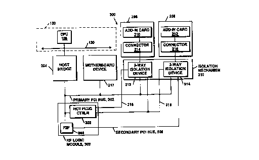
Figure 3 show as an improved hot plug arrangement 300 in
S accordance with an embodiment of the invention, in which newly inserted
adapter cards can be tested prior to connection to the primary PCI bus 202.
The hot plug arrangement 300 has a hot plug logic module 302 that
includes both a hot plug controller 302, and a secondary bridge 304, e.g., a
PCI-to-PCI bridge ("P2P") 304 connected between the primary PCI bus
and a secondary bus 306, e.g., a PCI bus. Moreover, the hot plug
arrangement 300 has three-way isolation switches 312, 314, described
below, for separately connecting (and disconnecting) the individual slots
206, 208 to (from) the primary PCI bus 202 and to (from) the secondary
local PCI bus 306. The switches 312, 314 are controlled by control signals
applied over control lines 316, 318 by the hot plug controller 303. Thus,
the hot plug arrangement 300 can connect a slot containing a newly
inserted adapter card to the secondary bus 306 for testing purposes to
confirm operation of the card within normal parameters before it connects
the card to the primary bus 202.
Unlike the conventional arrangement 200 of Figure 2,
communications between the host bridge 204 and either the hot plug
controller 303 or the individual slots 206, 208 is achieved directly via the
primary PCI bus for normal operation and through the secondary PCI bus
for testing. More specifically, for testing of individual slots,
communication between the host bridge 204 (and thus, e.g., CPU 105) and
individual slots 206, 208 is achieved through the P2P 304 and the
secondary PCI bus 306 on an individual slot basis (i.e., one slot at a time)
via the secondary PCI bus 306. The arrangement 300 preferably permits
communication between the host bridge 204 and the slots 206, 208 via only
- 10-
CA 02301477 2000-03-21
one of the primary and secondary buses 202, 306 at any given time. Under
these controlled conditions, the CPU 105 can probe an adapter card 206,
208 through the PCI-to-PCI ("P2P") bridge 304 to determine that it is fully
functional before the arrangement 300 places the adapter card on line by
enabling communication over the primary PCI bus 202.
Accordingly, hot plug insertion according to this embodiment of the
invention is a process of inserting an adapter card into a server or other
computer system by hot-plugging, under the control of the hot plug
controller 303. Hot plug insertion generally entails the following sequence
of steps: a) user notification, during which, through a hot-plug
administrative application's gui, a technician notifies the server that a hot
plug insertion will take place at a particular empty slot, e.g., slot 206; b)
power-down, during which, through the hot plug controller 303, the
server's operating system turns off the slot, if it is not already in an "off
1 S condition, preferably with a slot-state indicator showing that condition;
c)
isolation, during which, under the control of the hot plug controller 303,
the slot 206 is electrically isolated from the primary PCI bus 202 by the
isolation devices 312; c) insertion, during which the adapter card 210 is
physically inserted into the slot; d) verification, during which the server
100, through the hot plug controller 303, verifies that the adapter card 210
is inserted properly in the slot 206 by performing diagnostic and
performance tests over the secondary PCI bus 306; e) power-up, during
which, through the hot plug controller 303, the server's operating system
turns on, i.e., powers up, the slot and the newly-inserted adapter card 206,
with the slot-state indicator reflecting that condition; g) configuration,
during which, the server's operating system re-configures the system by
loading a device driver for the newly installed adapter card 210.
Hot plug removal is a process of removing an adapter card from a
computer server or other computer system by hot-plugging, under the
-11-
' CA 02301477 2000-03-21
control of the hot plug controller 303. Hot plug removal generally entails
the following sequence of steps: a) preparation, during which, through a
hot-plug administrative application's gui, a user indicates that a particular
adapter card, e.g., adapter card 210, will removed from a particular slot; b)
quiecence, during which, through the administrative application, the
server's operating system terminates any on-going processes that are
accessing the adapter card 210 and takes the appropriate software driver for
the adapter card 210 offline; c) power down, during which, through the hot
plug controller 303, the server's operating system cuts power to the slot,
with a slot-state indicator showing that the slot 206 is powered down and
that it is safe to proceed with removal of the adapter card 210; d) isolation,
during which, under the control of the hot plug controller 303, the slot 206
is isolated from the PCI bus signals by isolation devices 312; and e) card
removal, during which the adapter card 206 is physically removed from the
slot 206.
Figure 4 shows one embodiment of the hot plug controller 303
connected to the primary PCI buses 202. The hot plug controller 303
provides a software interface to sequence power, clocks and bus signals to
adapter cards that are being "live" inserted into or removed from slots 206,
208. The hot plug controller 303 includes a switch timing module 430, an
internal register module 432 for receiving, e.g., data and address signals,
and a clock control module 434 for controlling bus frequency, e.g. a
nominal 33 MHz or 66 MHz. The hot plug controller 303 also contains a
per-slot control module 436, 438, 440 for each slot that controls the power
and slot connection condition (e.g., up to a maximum of "m" slots). Each
of these slot control modules 436, 438, 440 is of the same basic
construction, so only signal lines for module 436 are shown in more detail.
The hot plug controller 303 contains a PCI interface to the PCI bus
303 for receiving signals from bus lines as specified by the PCI Spec,
-12-
' CA 02301477 2000-03-21
including (among other conventional lines not shown) the following lines
of significance herein: cycle frame (FRAME#), target ready (TRDY#),
initiator ready (IRDY#), bus access request (REQ#), bus access grant
(GNT#), and address/data lines (AD [31:0]). More specifically, FRAME#
is driven by a current bus master to indicate the beginning and duration of
an access. FRAME# is asserted to indicate that a bus transaction is
beginning. While FRAME# is asserted, data transfer continues. When
FRAME# is deasserted, the transaction is in the final data phase. IRDY#
indicates the initiating bus master's ability to complete a current data phase
of the ongoing transaction. IRDY# is used in conjunction with TRDY#; a
data phase is completed on any clock where both IRDY# and TRDY# are
asserted. The hot plug controller 303 is reset via a PCI RST# input.
During reset, M66EN inputs from the slots 206, 208 are sampled, and
CLK33/66 driven to select an appropriate bus frequency. The switch
timing module 430 is used to ascertain a specific bus time slot when the
primary PCI bus 303 is available and the slot can be turned "on" or "off'
and thereby connected to or disconnected from the PCI bus 303 by means
of the isolation mechanism 310.
To that end, in this embodiment, a combination of the REQ#,
GNT#, FRAME#, and IRDY# signals is used to control the timing of slot
connection and disconnection. The switch timing module 330 will assert
REQ# when the slot is ready for connection or disconnection. It will
initiate connection or disconnection when the GNT# is asserted by the host
bridge 204, and more particularly when the GNT#, FRAME#, and IRDY#
pins are LOW following REQ# being asserted.
Each slot control module 436, 438, 440 is connected to the
associated slot by the following signals lines: PWR ON/OFF, which turns
power "on" and "ofd' to the slot; SWITCH CONTROL, which causes the
isolation mechanism 310 to connect and disconnect the slot; PRSNT2#~and
-13-
' CA 02301477 2000-03-21
PRSNT 1 #, which indicate the presence or absence of an adapter card in the
slot; M66EN, which indicates whether the adapter card in the respective
slot can be operated at 66 MHz, and other conventional signal lines (not
shown). All of these signal lines are conventional, except as specifically
S noted herein with respect to the SWITCH CONTROL signal for certain
described embodiments.
Figure SA shows an isolation mechanism 500 in accordance with an
exemplary embodiment for implementing both of the three-way isolation
devices 312, 314 of Figure 3 in a single device supporting the two slots
206, 208. It should be understood that the illustrated two slot arrangement
is merely an example, though the number of slots utilized in this
embodiment is currently typical for 66 MHz buses. The invention can be
implemented in arrangements having more than two slots. The isolation
mechanism 500 incorporates a one-bit switch 502 for making the necessary
connections. The switch 502 connects one of the primary PCI bus 202 and
secondary PCI bus 306 to one of the slots, i.e., slot 1 (corresponding to slot
206 in Figure 3) and slot 2 (corresponding to slot 208 in Figure 3), via lines
504 and 506, respectively. Thus, each slot 206, 208 can be connected to
only one of the primary and secondary PCI buses 202, 306 at any time.
For example, both slots 206, 208 can be connected to the primary PCI bus
202; or both slots 206, 208 can be connected to the secondary PCI bus 306;
or slot 206 can be connected to bus 202 and slot 208 to bus 306, or visa
versa.
The one-bit switch 502 is controlled by an n-bit code provided over
control line 508, which in this embodiment replaces both control lines 316
and 318 of Figure 3. The n-bit code defines the specific connectivity of
the switching device 500, since only certain connections are necessary and
appropriate. For example, in Figure 6, only eight states are required to
control the two slots, and thus "n" can equal three (n=3) to optimize the
-14-
' CA 02301477 2000-03-21
number of pins, or "n" can equal four (n=4) for asynchronous decoding.
The switch 502 can be, for example, a commercially available FET switch,
or implemented as a custom-designed ASIC (application specific
integrated circuit). A switch available from Texas Instruments
Incorporated, Texas, USA, designated SN74CBT 16209 can be readily
adapted for use in this embodiment.
Figure SB shows a schematic of an exemplary ASIC implementation
of the switch 502 in the form of a crossbar switching fabric 512 under
control of a state decoder 514 responsive to an n-bit code. The switching
fabric 512 employs a circuit formed using FETs as switching elements for
connecting either the primary or secondary PCI bus to either of two slots,
designated slot 1 or slot 2. Actually, the hot plug controller 303 can
control the switching device 400 through a combination of Grey code,
and/or the slot control module 436 (Figure 4), in order to minimize any bus
contention. The state decoder 514 causes the switching fabric 512 to enter
into a particular one of the states described below in response to the
insertion, removal and testing of an add-in card. In the state names below,
"OFF" indicates isolation, "ON" indicated connection, and "TST" indicates
testing.
DESCRIPTION OF STATE TRANSITIONS
State Name Connection Descri tp ion
lOFF 20FF None All busses and slots
isolated.
lON 20N Primary PCI-Slot 1 and Both slots
connected to Primary PCI bus.
Primary PCI-Slot 2
-15-
' CA 02301477 2000-03-21
1TST 20FF Secondary PCI-Slot 1 Slot 1 accessed for
testing;
Slot 2 is isolated.
l ON 20FF Primary PCI -Slot 1 Slot 1 connected to
Primary PCI
Slot 2 is isolated.
lOFF 2TST Secondary PCI-Slot 2 Slot 2 accessed for
testing;
Slot 1 is isolated.
lOFF 20N Primary PCI-Slot 2 Slot 2 connected to
Primary PCI;
Slot 1 is isolated.
1TST 20N Secondary PCI-Slot 1 and Slot 1 accessed for testing;
Primary PCI-Slot 2 Slot 2 connected to
Primary PCI.
lON 2TST Secondary PCI-Slot 2 and Slot 2 accessed for testing;
Primary PCI-Slot 1 Slot 1 connected to
Primary PCI.
Figure 6 shows a state transition diagram in accordance with a
preferred embodiment, illustrating state transitioning of the switch device
502 under the control of the hot plug controller 302 to provide sound
operation and avoid switch glitches. Starting at state A at the top of the
diagram, with both busses and slots isolated, if a card 1 is inserted into
slot
1, the hot plug controller 302 causes the switch to transition to state B. In
state B, the card 1 is tested while slot 2 remains off. If the test fails, the
hot
plug controller 302 causes the switch to return to state A. On the other
hand, if card 1 passes, the hot plug controller 302 causes the switch to enter
state C, where slot 1 and slot 2 remain isolated, and signals the CPU that
-16-
CA 02301477 2000-03-21
card 1 is ready to be connected (or brought on-line). After that, the hot
plug controller 302 causes the switch to transition to state D, in which slot
1 is connected and slot 2 remains in an isolated condition. If, while the
switch is in state D, card 1 needs to be removed, the hot plug controller 302
causes the switch to transition to state A, and await a further change with
respect to insertion or removal of cards in the slots.
If the switch is in state D and a card 2 is inserted in slot 2, the hot
plug controller 302 causes the switch to transition to state E. In state E,
the
card 2 is tested while slot 1 remains ON, i.e., connected. If the test fails,
the hot plug controller 302 causes the switch to return to state D. On the
other hand, if card 2 passes, the hot plug controller 302 causes the switch to
enter state F, where slot 1 is connected and slot 2 remains isolated, and
signals the CPU that card 2 is ready to be brought on-line. After that, the
hot plug controller 302 causes the switch to transition to state G, in which
slot 1 and slot 2 are both connected. If, while the switch is in state G, card
2 needs to be removed, the hot plug controller 302 causes the switch to
transition to state D, and await a further change with respect to insertion or
removal of cards in the slots.
Starting again at state A at the top of the diagram, with both busses
and slots isolated, if a card 2 is inserted into slot 2, the hot plug
controller
302 causes the switch to transition to state H. In state H, the card 2 is
tested while slot 1 remains off. If the test fails, the hot plug controller
302
causes the switch to return to state A. On the other hand, if card 2 passes,
the hot plug controller 302 causes the switch to enter state I, where slot 1
and slot 2 remain isolated, and signals the CPU that card 1 is ready to be
brought on-line. After that, the hot plug controller 302 causes the switch to
transition to state J, in which slot 2 is connected and slot 1 remains in an
isolated condition. If, while the switch is in state J, card 2 needs to be
removed, the hot plug controller 302 causes the switch to transition to state
-17-
' CA 02301477 2000-03-21
A, and await a further change with respect insertion or removal of cards in
the slots.
If the switch is in state J and a card 1 is inserted in slot 1, the hot
plug controller 302 causes the switch to transition to state K. In state K,
the card 1 is tested while slot 2 remains ON, i.e., connected. If the test
fails, the hot plug controller 302 causes the switch to return to state J. On
the other hand, if card 1 passes, the hot plug controller 302 causes the
switch to enter state L, where slot 1 is isolated and slot 2 remains
connected, and signals the CPU that card 1 is ready to be brought on-line.
After that, the hot plug controller 302 causes the switch to transition to
state G, in which slot 1 and slot 2 are both connected. If, while the switch
is in state G, card 2 needs to be removed, the hot plug controller 302 causes
the switch to transition to state J, and await a further change with respect
to
insertion or removal of cards in the slots.
Other Embodiments
As alternative embodiments to that shown in Figures 3, a hot plug
controller can have any of a number of different bridges for interfacing the
primary bridge with the secondary bridge ("X2X", where X is a specified
type of bus). For example, where the primary bus is a PCI bus, the
invention can be implemented using a "P2X" bridge, such as a PCI-to-
JTAG, PCI-to-I2C, or PCI-to-ISA (where "JTAG" stands for IEEE 1149.1
Standard Test Access Port (further described below), "I2C" stands for Inter
Integrated Circuit bus, and "ISA" stands for Industry Standard
Architecture). The desirability of each of these approaches depends on the
application involved; some of these approaches could permit physically
smaller implementations, some may limit adapter card testing capability,
and some may require more overhead than others.
-18-
CA 02301477 2000-03-21
Figure 7A shows a hot plug arrangement 700 in accordance with an
alternative embodiment of the invention, using a JTAG serial interface 702
between the hot plug controller and the isolation devices 312, 314.
"JTAG" is further described in IEEE 1149.1 - 1990, Standard Test Access
Port and Boundary-Scan Architecture ("JTAG Spec"), which is
incorporated herein by reference, and available from IEEE, 3 Park Avenue,
17'~ Floor, NY, NY, 10016-5997, USA. The circuitry and test logic
defined in the JTAG Spec allows test instructions and associated test data
to be fed into an adapter card and, subsequently, allows the results of the
execution of the instruction to be read out. The hot plug controller 704 in
the illustrated JTAG arrangement 700 can decode PCI transactions on the
primary PCI bus targeted as 'test' accesses to a particular slot, and then
encode the PCI transaction into a serial stream to send to the appropriate
isolation devices 312, 314 (for example, implemented as the isolation
mechanism 750 of Figure 7C). The isolation devices 312, 314 would then
decode the serial stream back into PCI conventional signals and execute the
transaction, clock cycle by clock cycle. Although this approach may be
more time consuming and will not test a newly inserted adapter card at full
speed, complete functional testing is possible. Hot plug arrangement 700
may be advantageous also in that it lends itself to implementations having
minimized controller pin count.
Figure 7B . shows an illustrative embodiment of the hot plug
controller 704 for use in the JTAG-based arrangement 700 of Figure 7A.
The hot plug controller 704 can be essentially the same as Figure 4, except
that it includes a JTAG controller 730 for providing as output a serial
stream of commands in accordance with JTAG standard protocols, and a
switch control signal, for example, in the form of an n-bit code, as
described above.
-19-
CA 02301477 2000-03-21
Figure 7C shows a three-way isolation mechanism 750 for use in the
JTAG-based arrangement 700 of Figure 7A. The switch 502 is controlled
by an n-bit code, as noted above, for selectively interconnecting the
primary PCI bus 752 or JTAG test lines 754 to either slot 1 or slot 2. A
test access port ("TAP") 756 decodes a serial stream input of commands
from the JTAG controller 730 (Figure 7B), including the n-bit code. The
TAP 756 loads the decoded results into a register 758. The register 758
will thus contain a test bit pattern, which is applied during a single clock
cycle of clock 759 to a JTAG test lines 754 connected as input to the
switch 502, and via the switch to selected contacts of a newly inserted
adapter card (not shown) received in either slot 1 or slot 2. The register
758 will also contain and then apply the n-bit code to a control terminal
760 of the switch 502 during the same clock cycle. The results of the test
are returned via the switch 502 responsive to another n-bit code, through
1 S JTAG lines 756 and placed in the register 758 and then passed to the JTAG
controller 730 via the TAP 752.
Figure 8A shows a hot plug arrangement 800 in accordance with yet
another alternative embodiment of the invention. The hot plug
arrangement 800 has a hot plug controller 802, which is connected to a host
bridge 804 by a pair of request (REQ) and grant (GNT) lines constituting
arbitration lines for the primary PCI bus 202, in the same manner as any
other PCI device. An I2C bus (I2C) connects the host bridge 804 to the hot
plug controller 802 for configuring and controlling the hot plug controller
802. Preferably, the hot plug controller 802 is not otherwise connected to
the primary PCI bus lines; however, the hot plug controller 802 also
communicates with the host bridge 804 through a special port into the PCI
arbiter 806, via a special signal line, BUS IDLE. The BUS IDLE signal is
generated, for example, by combinational logic 808 in the host controller
804, and is asserted when the primary PCI bus 302 is idle (i.e., no bus
-20-
i
CA 02301477 2000-03-21
transaction), which occurs when both FRAME# and IRDY# are HIGH. In
this embodiment, under software control, the hot plug controller 802
performs the following steps in enabling of the isolation devices 312, 314:
A) assert REQ# to the host bridge, requesting control of the PCI
bus;
B) wait for the host bridge to assert GNT#, indicating that the HPC
is the next master allowed use of the PCI bus;
C) wait for the BUS IDLE to be asserted by the host bridge,
indicating that the previous master has relinquished the PCI
bus, that no other master will be allowed onto the PCI bus,
and that this condition will continue for a pre-determined
number (e.g., 16) of clock cycles. During the 16 clock
cycles, the hot plug controller will enable the isolation
devices and de-assert REQ#.
As described, this implementation can avoid placing additional
loading on any of the shared signals of the PCI bus, such as FRAME# and
IRDY#, while providing hot plugging capability. The overhead for this
arrangement amounts to only an additional BUS IDLE pin off the host
bridge 804, and a simple logic circuit for generating the BUS IDLE signal.
Further, since the interface to the host bridge 804 is through dedicated
point-to-point signals, the host plug controller 802 and the host bridge 804
can be placed at a relatively long distance apart, allowing system designs
with separate input/output (I/O) boards.
Figure 8B shows an illustrative embodiment of the hot plug
controller 802 for use in the hot plug arrangement 800 of Figure 8A. The
hot plug controller 802 can be essentially the same as Figure 4, except that
it includes a BUS IDLE input to the switch timing module 430, and an I2C
bus input to the internal registers 432 instead of the AD [31:0} input lines.
-21 -
_. __._._-,_,_._ ., CA 02301477 2000-03-21
Although an exemplary embodiment of the invention has been
disclosed, it will be apparent to those skilled in the art that various
changes
and modifications can be made which will achieve some of the advantages
of the invention without departing from the spirit and scope of the
invention. It will be obvious to those reasonably skilled in the art that
other components performing the same or equivalent functions may be
suitably substituted. Further, various techniques of the invention may be
achieved in either all software implementations, using appropriate
processor instructions, or in all hardware logic implementations, or in
hybrid implementations that utilize a combination of hardware logic and
software logic to achieve the same or equivalent results. Further, aspects
such as specific configuration of logic and/or instructions utilized to
achieve a particular function, as well as other modifications to the
inventive concept are intended to be covered by the appended claims.
~a