Note: Descriptions are shown in the official language in which they were submitted.
CA 02302013 2000-02-25
WO 99/10792 PCTIUS98/17608
INTEGRATED DRAM WITH HIGH SPEED INTERLEAVING
FIELD OF THE INVENTION
This invention relates generally to the field of digital memory systems.
BACKGROUND OF THE INVENTION
High performance data processing systems require digital memory systems which
are
capable of storing and providing large amounts of data at very high speeds.
For example,
graphics controllers which operate in conjunction with a host computer to
perform sophisticated
image manipulation and rendering functions to generate data for display on a
display screen,
require memories which are capable of storing and providing the amount of data
required of
such functions at very high data rates.
Dynamic Random Access Memories (DRAMS) are often used to meet the storage
requirements required by high performance systems. DRAMS are typically
characterized by a
greater storage density per chip when compared to static random access
memories (SRAMs).
However, DRAMS are also typically characterized by slower access times then
SRAMs.
A variety of techniques have been used to increase the bandwidth of digital
memory
systems employing DRAMS. For example, the memory, and the data paths to and
from the
memory, may be organized to allow multiple words of data to be retrieved in a
single access.
Although such a technique provides increased bandwidth, there remains a need
for digital
memory systems which provide even greater data storage and data throughput
than is currently
available.
SUMMARY OF THE INVENTION
In a principle aspect, embodiments of the present invention provide a memory
system
capable of providing data at high rates. Presentation of a row address to the
mcmory system
results in a row of data being read out of parallel storage arrarys in the
memory system by a
plurality of Bit-Line Sense Amplifiers (BLSA). Presentation of a column
address to the
memory system causes selection of a corresponding column of data in the
selected row. The
selected column of data is retrieved in two phases by toggling of the least
significant bit of the
column address. Advantageously, the signals in the memory system are of the
small signal
differential type of signal produced by the BLSAs, and are not amplified by
main sense
amplifiers (MSA) until selection of each of the subsets or phases for output.
This advantageous
feature allows a reduction in the number of MSAs required for the memory
system. The result
is fewer hardware elements, fewer routing lines to connect such components and
lower power
*rB
CA 02302013 2005-04-27
consumption. A farther advantage is that output of the selected column in two
subsets or
phases results in higher data throughput by allowing the least significant
column address bit to
be switched at a rate approximately twice as fast as the column address. This
feature provides
the advantage of allowing simple and more direct routing of the single, least
significant bit of
the column address for higher speed switching. The lower frequency switching
required of the
column address imposes fewer constraints on the routing of the column address
signals in the
IC chip, thus reducing design complexity.
Accordingly, in one aspect of the present invention there is provided an
integrated
circuit comprising:
a graphics controller which generates a row address signal, first and second
column
address signals for each row signal and which switches a hi/lo signal for each
column address
signal, to read a plurality of data words from a memory;
said memory comprising a Dynamic Random Access Memory (DRAM) which
comprises,
a plurality of arrays, organized into an odd bank and an even bank, each array
including a plurality of rows and a plurality of columns;
a pair of bit-line sense amplifiers, a first of said bit-line sense amplifiers
corresponding to said odd bank and a second of said bit-line sense amplifiers
corresponding to
said even bank;
a row decoder which selects one of said rows in accordance with said row
address
received from said graphics controller, to transfer bits in a selected row to
said first and said
second bit-line sense amplifiers;
a column decoder which selects a pair of columns in said selected row in
accordance
with said first and said second column address received from said graphics
controller; and
a pair of multiplexers, a first of said multiplexers coupled to receive data
from said
first bit-line sense amplifier and a second of said multiplexers coupled to
receive data from
said second bit-line sense amplifier, said multiplexers responsive to said
hi/lo signal generated
by said graphics controller to select a first subset of bits stored in each of
said bit-line sense
amplifiers to generate a first data output word from said first column address
in response to a
first state of said hi/lo signal, and responsive to a change in value of said
hi/lo signal for
selecting a second subset of bits stored in each of said bit-line sense
amplifiers to generate a
second data output word from said first column address.
According to another aspect of the present invention there is provided a
memory
system comprising:
a plurality of memory arrays, each of said arrays comprising a plurality of
rows, and a
plurality of columns, each of said columns comprising a plurality of mufti-bit
memory words;
2
CA 02302013 2005-04-27
a row address decoder responsive to a row address for selecting one of said
plurality of
rows;
a column address decoder responsive to a column address for selecting one of
said
plurality of columns;
a pair of sense amplifiers responsive to said selected row for storing data
contained in
said row;
a selector which responds to a first value of a hi/b signal to select a first
sub-group of data,
corresponding to said column address, stored in each of said bit-line sense
amplifiers and to a
second value of said h/b signal to select a second sub-group of data,
corresponding to said
column address, stored in each of said bit-line sense amplifiers.
According to yet another aspect of the present invention there is provided a
memory
system comprising:
an odd memory bank and an even memory bank each of said banks comprised of at
least one memory array arranged in a plurality of rows and columns;
a row address decoder which responds to a row address to select one of said
rows of
said odd and even memory banks;
an odd bit-line sense amplifier responsive to data bits in said selected row
in said odd
memory bank and an even bit-line sense amplifier responsive to data bits in
said selected row
in said even memory bank;
a column address decoder which responds to a column address to select a column
of
data bits from said odd bit-line sense amplifier and said even bit-line sense
amplifier; and
an odd set of multiplexers, responsive to a HI/LO signal, which selects a
first subset of
said column of data bits selected from said odd bit-line sense amplifier; and
an even set of multiplexers, responsive to said HI/LO signal, which selects a
second
subset of said column of data bits selected from said even bit-line sense
amplifier.
According to still yet another aspect of the present invention there is
provided an
integrated circuit comprising:
a graphics controller which generates a row address signal, a column address
signal
and which switches a hi/lo signal corresponding to said column address signal,
to read a
plurality of data words from a memory;
said memory comprising a Dynamic Random Access Memory (DRAM) which
compnses,
an odd memory bank and an even memory bank each of said banks comprised of at
least one memory array arranged in a plurality of rows and columns;
a row address decoder which responds to a row address to select one of said
rows of
said odd and even memory banks;
2a
CA 02302013 2005-04-27
an odd bit-line sense amplifier responsive to data bits in said selected row
in said odd
memory bank and an even bit-line sense amplifier responsive to data bits in
said selected row
in said even memory bank;
a column address decoder which responds to said column address to select a
column of
data bits from said odd bit-line sense amplifier and said even bit-line sense
amplifier; and
an odd set of multiplexers, responsive to said hi/lo signal, which selects a
first subset
of said column of data bits selected from said odd bit-line sense amplifier;
and
an even set of multiplexers, responsive to said hi/lo signal, which selects a
second
subset of said column of data bits selected from said even bit-line sense
amplifier.
These and other features and advantages of the present invention may be better
understood by considering the following detailed description of a preferred
embodiment of the
invention. In the course of this description, reference will frequently be
made to the attached
drawings
BRIEF DESCRIPTION OF THE DRAWINGS
Figure 1 is a high-level block diagram of a graphics controller chip which
employs the
princip 1 a of the present invention.
Figure 2 is a block diagram of a preferred embodiment of the memory system of
Figure 1.
Figure 3 is a timing diagram showing operation of a preferred embodiment.
DETAILED DESCRIPTION
In Figure 1 of the drawings, a graphics controller is implemented in an
Integrated
Circuit (IC) 100 which includes a controller 102 and a memory 104. The
graphics controller
preferably operates in conjunction with a microprocessor (not shown) to
receive data and
commands from the microprocessor to store data in the memory 104, to
manipulate the data
via the controller 102 and to display the data onto a visual display (not
shown) by generation
of appropriate control signals. An example of the functions performed by the
controller is
provided in a data book published by S3 Incorporated of Santa Clara,
California, entitled
YiRGE Integrated 3D AccE~lerator, published August 1996. This data book
describes many of
the functions performed by the ViGRE graphics accelerator chip sold by S3
Incorporated.
Memory 104 preferably takes the form of a Dynamic Random Access Memory
(DRAM). In a preferred embodiment the controller 102 and the memory 104 are
coupled by a
data path which is 128 bits wide allowing transfers between the controller and
the memory of
128 bits per clock cycle. T'he memory 104 stores and outputs data in response
to control
signals generated by the controller 102.
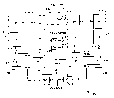
Figure 2 of the drawings is a block diagram illustrating further details of
the memory
104. The memory 104 includes a plurality of storage arrays 202, 203, 204, 205,
206, 207, 208
2b
CA 02302013 2000-02-25
WO 99/10792 PCT/US98/17608
and 209 which are alike in structure and storage capacity. The storage arrays
202-209 are
organized in two banks 211 and 212 which may be referred to as an odd bank and
an even bank,
respectively. The storage arrays are conventional DRAM type storage arrays
which employ a
one transistor-one capacitor per cell structure to achieve high density. In a
preferred
embodiment, each of the storage arrays 202-209 contains 256 rows each
containing lKbits.
Thus, each bank 211, 212 stores 256 x 1k x 4 = lMbit of data, for a total
memory capacity
between the two banks of 2Mbits.
The data stored in the storage arrays is accessed by decoding a row address
with decoder
214. In a preferred embodiment the row address is 8 bits to correspond to 256
rows in the banks
211 and 212. The row address is stored in a register 213 in response to a Row
Address Strobe
(ItAS) signal generated by controller 102. The decoder 214 selects one of 256
rows in the
storage arrays 202-209 to be read out by two sets of bit-line sense amplifiers
(BLSA) 216 and
218.
The row address decoded by decoder 214 is supplied to each array of each bank
to
generate a row of data which is 8k bits wide. BLSA 216 senses and amplifies
the data stored in
the storage cells contained in the odd half 211 of the mw selected by mw
decoder 214. BLSA
218 operates similarly with even half of the row selected in bank 212.
A column address received from controller 102 is stored in register 219, in
response to a
Column Address Strobe (CAS) signal from controller 102. The column address in
register 219
is decoded by a decoder 220 to select 256 bits from the 8k bits stored in BLSA
216 and 218.
Muitiplexers 220 and 222 perform a two-to-one multiplexing function.
Multiplexer 220
receives 128 bits from SA 216 into 64 pairs of two-to-one multiplexers.
Multiplexer 222 is
similarly organized and operates in a similar manner with respect to SA 218.
Multiplexers 220
and 222 are both controlled by a HI/LO signal generated by the controller 102.
The HI/LO
signal corresponds to the least significant bit of the column address. Once
BLSAs 216 and 218
have sensed and amplified the data in each of the storage cells of the
selected row, 128 bits of
data representing a half column of data are available to the controller 102
from the memory 104.
As can be seen from Figure 2, each 128-bit quantity of data provided by memory
104 consists of
64 bits of data from odd bank 211 and 64 bits of data from even bank 212. Once
the controller
102 has captured the first 128 bits of data, the HI/LO signal is toggled to
change its value from a
binary 0 to a binary 1, or alternatively from a binary 1 to a binary 0, to
cause multiplexers 220
and 222 to select the other 64 bits of data received from BLSAs 216 and 218,
respectively.
As can be seen, toggling of the HI/LO signal causes another 128 bits of data
to be
outputted by the memory 104. Use of the HI/LO signal to retrieve an additional
128 bits of
3
CA 02302013 2000-02-25
WO 99/10792 PCTNS98/17608
information is advantageous in that only one signal needs to be toggled to
generate an additional
128 bits of data instead of changing of an entire address bus. This simplifies
routing of the IC
chip 100 by allowing the single HI/LO signal to be designated as a critical
path and to be routed
on the IC chip 100 in an optimal manner to allow for higher frequency
switching, than would be
possible for the row address lines or the column address lines.
Data selected by multiplexers 220 and 222 is amplified by an odd and even set
of Main
Sense Amplifiers (MSA) 224 and 226. The MSAs 224 and 226 are conventional and
are also
commonly known as data sense amplifiers. The MSAs 224 and 226 operate in a
conventional
fashion to convert the small (differential) type signal generated by BLSA's
216 and 218 into full
swing signals useable by the controller 102.
The foregoing description has focused on a read operation in which data is
retrieved
from the memory 104. A write operation operates similarly in all respects
except that a write
enable signal is generated by controller 102 and data is provided to the
memory 104 for writing
into the storage arrays. The MSA's 224 and 226 convert the received full swing
data signals
into small signals. The resulting signals are then written into the
appropriate location in banks
211 and 212 in response to appropriate row and column addresses, RAS and CAS
signals and
the write enable signal. In Figure 2 the write enable signal is shown
generally. Control of the
memory system including the data paths internal to the system to distinguish
between read and
write operations is conventional and will be understood by those skilled in
the art in view of the
present disclosure.
Figure 3 of the drawings is a timing diagram showing the relationship of the
signals sent
by controller 102 to memory 104 to obtain four data words. The data, address
and control
signals generated by the controller 102 are generated synchronously with a
clock signal
designated in Figure 3 as CLKC, and shown at 302. A Write Enable (WE) signal
shown at 304
controls whether a memory operation is for reading or for writing. The Write
Enable signal is
shown as an active low signal, meaning that when it has a logical 0 value, it
controls the writing
of data into the memory 104, and when it has a logical 1 value, it is inactive
and data is then
read from memory. The row address to the memory is shown at 306 and as
explained above,
preferably comprises 8 bits to select one of 256 rows. Use of the row address
306 by the
memory 104 is controlled by the RAS signal 305 which causes the mw address to
be stored into
register 213. The column address signal as noted above preferably comprises 6
bits and is
shown at 308. Use of the column address is controlled by the CAS signal shown
at 307, which
causes the column address to be stored in register 219. The HI/LO signal is
shown at 310. Data
outputted by the memory 104 is shown at 312.
4
*rB
CA 02302013 2000-02-25
WO 99/10792 PCT/US98117608
The timing diagram of Figure 3 shows a read operation. The read operation
takes eight
clock cycles as shown by the individually numbered clock signals at 302. In
the cycle before
cycle 0, a row address is placed onto the row address bus by the controller
102 and the RAS
signal is asserted to store the row address into the register 213. In clock
cycle 2, after a
sufficient amount of time has been allowed for the row address to be decoded
and to allow the
data in the decoded row to be sensed into the sense amplifiers 216 and 218,
the column address
is provided to select one of the two columns in the selected row and the CAS
signal 307 is
asserted to cause the column address to be stored. The CAS signal as seen is
asserted at cycle 2.
At cycle 4, the first 128 bits of data becomes available in the selected row.
At cycle 3, the
HI/LO signal is toggled to cause the second 128 bits of data to become
available at cycle S.
Also at cycle 5, the column address is changed to select the second column of
data stored in the
sense amplifiers 216 and 218. This causes a third 128 bits of data to become
available at cycle
6, during which cycle the HI/LO signal is toggled once again to cause a fourth
128 bits of data
to become available in cycle 7. The second column address may be but need not
be sequential
to the first address. Once the second column address has been asserted at
cycle 5, in the
following cycle RAS and CAS are deactivated as they are no longer needed. This
allows
another memory cycle to start at cycle 9. As seen from the timing diagram of
Figure 3, a total of
512 bits of data are accessed by using the single row address. The HI/LO
signal is toggled at a
frequency which is twice the frequency at which the column address is required
to change. This
reduces the number of critical paths required in the memory 104 and allows the
frequency of the
clock to be increased in comparison to using four different column addresses
to retrieve the
same amount of data.
It is to be understood that the specific mechanisms and techniques which have
been
described are merely illustrative of one application of the principles of the
invention. For
instance, the specific widths of data paths and the size of the memory arrays
described herein are
provided merely to assist in explanation of an exemplary embodiment. Other
widths and sizes
are well within the scope of the principles of the invention. Numerous
additional modifications
may be made to the methods and apparatus described without departing from the
true spirit and
scope of the invention.
5