Note: Descriptions are shown in the official language in which they were submitted.
20365-4 117 CA 02302020 2000-07-12
1
INTERFACE CIRCUIT FOR FULL-CUSTOM AND SEMI-CUSTOM CLOCK DOMAINS
BACKGROUND OF THE INVENTION
Field of the Invention
The subject matter of the application is directed to
an integrated circuit having both analog and digital circuit
parts.
Description of the Prior Art
High-complexity integrated circuits ICs with an
analog circuit part FC (full-custom) and a digital circuit SC
(semi-custom) have a plurality of clock domains. The semi-
custom part generally contains a clock domain in the form of a
clock tree. The full-custom part contains a plurality of clock
domains. A realization of the clock domains of the full-custom
part in the form of a clock tree, however, is of the question
due to the non-regular layout structure of the full-custom
part, the punctually required highly punctual driver capability
and a special consideration of running times also referred to
as specified timing in the art that is sometimes required
between the various full-custom clock domains.
Given the transfer of several hundred data signals
from the full-custom to the semi-custom clock domain and vice
versa, difficulty arises in the exact simulatability an
infringement-free design of setup and hold time given the
simultaneous testability of the interface signals.
In semi-custom part, the gate selection is not
performed until the conversion of the Very-High Speed
Integrated Circuit Hardware Description Language (VHDL) code.
These gates are located in the layout via a place & route
20365-4 117 CA 02302020 2000-07-12
2
algorithm. An individual timing is thus required for every
individual semi-custom input/output signal I/O. Exact timing
simulations based on layout data given an extremely high
plurality of locally scattered I/0 signals is not possible.
Moreover, the driver dimensioning of each full-custom
output signal must be individually oriented to the semi-custom
gate to be driven, the input capacitance thereof and the
delivery lead. These values, however, are not completely
available until after the place & route algorithm, i.e. until a
very late design stage.
The subject matter of the present application is
based on the problem of overcoming the difficulties that have
been addressed.
SUMMARY OF THE INENTION
The subject matter of the application at least solves
the above problems by utilizing an interface connected between
an analog circuit section and a digital circuit section in an
integrated circuit, wherein the interface is configured to time
the forwarding of the data signals between the sections based
on a particular clock signal and output the data signal from
the interface based another clock signal.
The subject matter of the application exhibits an
advantage of:
employment of characteristic standard cells, as a
result of a closed loop. Thus, the complete and exact timing
simulation of the semi-custom part based on the extracted
layout data is possible.
CA 02302020 2006-04-24
20365-4117
3
In addition due to the prescription of the interface
gates and their position in the layout, the dimensioning of the
corresponding full-custom gates and their drivers specifically,
is drastically simplified on the basis of defined line lengths
and loads.
According to one aspect of the present invention,
there is provided an integrated circuit comprising: an analog
circuit section constructed substantially of analog circuitry
and having a first clock domain generating a first clock
signal; a digital circuit section constructed substantially of
digital circuitry and having a second clock domain generating a
second clock signal; and an interface connected between the
analog circuit section and the digital circuit section, the
interface configured to forward a data signal from the digital
circuit section to the analog circuit section based on the
second clock signal and to output the data signal to the analog
circuit section based on the first clock signal.
According to another aspect of the present invention,
there is provided an integrated circuit comprising: an analog
circuit section constructed substantially of analog circuitry
and having a first clock domain generating a first clock
signal; a digital circuit section constructed substantially of
digital circuitry and having a second clock domain generating a
second clock signal; and an interface connected between the
analog circuit section and the digital circuit section, the
interface configured to forward a data signal from the analog
circuit section to the digital circuit section based on the
first clock signal and to output the data signal to the digital
circuit section based on the second clock signal.
According to still another aspect of the present
invention, there is provided an integrated circuit comprising:
an analog circuit section constructed substantially of analog
CA 02302020 2006-04-24
20365-4117
' 3a
circuitry and having a first clock domain generating a first
clock signal; a digital circuit section constructed
substantially of digital circuitry and having a second clock
domain generating a second clock signal; and an interface
connected between the analog circuit section and the digital
circuit section, the interface configured to forward a first
data signal from the analog circuit section to the digital
circuit section based on the first clock signal and to output
the first data signal to the digital circuit signal based on
the second clock signal, and the interface also configured to
forward a second data signal from the digital circuit section
to the analog circuit section based on the second clock signal
and to output the second data signal to the analog circuit
section based on the first clock signal.
DESCRIPTION OF THE DRAV~IINGS
Figure 1 illustrates a schematic of the integrated
circuit of the present application.
Figure 2 shows a fundamental illustration of the
circuit of the interface I shown in Figure 1.
Figure 3 illustrates the circuit fc_scl shown in
Figure 2.
Figure 4 illustrates circuit fc-scl as shown in
Figure 2.
Figure 5 illustrates circuit sc_fc as shown in Figure
2.
Figure 6 illustrates a clock delay circuit by which
signal CK-FC is delayed by fixed phase shift 2 produced clock
signal CK DELAY.
CA 02302020 2006-04-24
20365-4117
' 3b
DESCRIPTION OF THE PREFERRED EMBODIMENTS
Identical reference characters in the Figures refer
to identical elements.
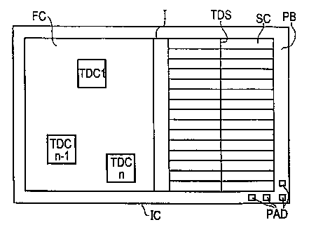
Figure 1 shows the layout of an integrated circuit IC
that has a complex structure with, for example, 3 million
transistors. The integrated circuit comprises a circuit
section SC (semi-custom), which is implemented essentially in
digital circuit technology and referred to below as digital
20365-4 117 CA 02302020 2000-07-12
4
circuit section, as well as a circuit section FC (full-custom),
which is implemented essentially in analog circuit technology
and is referred to below as analog circuit section. At its
edge, the integrated circuit comprises a pad area PB wherein
only a few contacting surfaces PAD are arranged by way of
example in Figure 1. The digital circuit section SC comprises
a clock domain TDS that, as shown in the drawing, can be
arranged as a clock tree. The analog circuit section FC
comprises a plurality of clock domains TDC1,...,TCn-1 and TDCn.
According to the application, an interface I is arranged
between the digital circuit section and the analog circuit
section. A signal that is to be forwarded from the digital
circuit section to the analog circuit section or from the
analog circuit section to the digital circuit section is
forwarded via the interface I. In a specific embodiment of the
subject matter of the application, all signals to be forwarded
from one circuit section to the other circuit section are
forwarded via the interface I. In a preferred embodiment of
the subject matter of the application, all signals to be
forwarded from the digital circuit section to the analog
circuit section as well as all signals to be forwarded from the
analog circuit section to the digital circuit section are
forwarded via the interface I. The circuit blocks fc sc 0,
fc-sc 1 or, sc-fc as shown in Figure 2 are combined to form an
overall interface and are arranged on the integrated circuit at
a central location between the digital circuit section and the
analog circuit section.
Figure 2 shows further details of the interface I. A
circuit block fc-sc 0 or fc-sc 1 is provided for forwarding a
signal DIN-(i-1), DIN-(i) from the analog circuit section to
the digital circuit section. A circuit block sc-fc is provided
for forwarding a signal from the digital circuit section to the
20365-4 117 CA 02302020 2000-07-12
analog circuit section. The circuit blocks fc-sc or,
respectively, sc-fc are provided in a number that corresponds
in number to the plurality of signals to be forwarded. Each
circuit block receives a first clock signal CK FC, a second
5 clock signal CK-SC, a signal TEST and an activation signal
SCAN EN. The signal TEST is considered activated when it
exhibits a high signal level "1". Each circuit block includes
an input SCAN-IN. An output D OUTSC of a circuit block fc-sc 1
for example is connected to the input SCAN-IN of another
circuit block fc sc 0.
The first clock signal CK FC and the second clock
signal CK_SC operate at the same frequency and have a phase
shift by half a clock period relative to one another. This
phase shift is accomplished by the circuit shown in Figure 6,
to be described later.
Figure 3 shows further details of a circuit block
fc sc 0. A flip-flop FF1 has its data input supplied with a
data signal D-IN delivered from the analog circuit section and
has the first clock signal CK_FC supplied to its trigger input.
A gate AND realizing the logical AND function has its input
side supplied with the signal output by the flip-flop FF1 at
its output side and with the inverted TEST signal. A data
multiplexer MUX has its input side supplied with the signal
output by the gate AND at its output side and with the SCAN-IN
[sic] signal. Based on the state of the signal SCAN EN, one of
the two signals supplied to the input side of the data
multiplexer is connected through to the output.
A flip-flop FF2 has its data input supplied with the
signal output by the data multiplexer at its output side and
has the second clock signal CK SC supplied to its trigger
input. The signal D OUTSC and the signal D OUT are supplied at
20365-4 117 CA 02302020 2000-07-12
6
the output of the flip-flop FF2, whereby the signal D OUT is
intermediately amplified via a buffer B.
It is assumed that, when, the signal TEST is at a low
signal level "0", as a result of not being activated, the
signal supplied to the other input of the gate AND is through-
connected. Also, signal SCAN EN is assumed to be in a state
where the signal supplied from the AND gate is through-
connected. The signal D-IN is taken with the clock signal
CK-FC from the flip-flop FF1 and supplied to the flip-flop FF2.
The signal D-IN is supplied from the flip-flop FF2 to the
digital circuit section with the clock signal CK SC.
When the signal TEST is at a high signal level "1",
as a result of being activated, the gate realizing the logical
AND function always outputs a low signal level "0" at its
output side regardless of the signal level at its other input.
This low signal level then also forms the signal D OUTSC and
the signal D OUT. Hence as a result of an activated signal
TEST, the signals D OUT at the outputs of all circuit blocks
fc-sc 0 can be set to a low signal level "0". The signal TEST
in Figures 3 and 4 generates predefined signals at the input of
the digital circuit section, making possible a separate test of
the semi-custom part as a result.
When the signal SCAN EN is at state where the signal
SCAN-IN [sic] is through-connected by the data multiplexer MUX,
it is forwarded from one to the next circuit block fc sc 0,
fc_sc 1 or, respectively, sc-fc. The signal SCAN-IN supplied
to the first circuit block thus appears at the outputs of all
circuit blocks fc_sc 0, fc_sc 1, sc_fc. All FF outputs D OUTSC
can be connected in series via the signal SCAN EN, the
multiplexer MUX and the flip-flop FF2 as a scan path. The
20365-4 117 CA 02302020 2000-07-12
7
connected scan path enables the monitoring of all interface
data signals.
Differing from the circuit block fc sc 0 shown in
Figure 3, a circuit block fc-sc 1 shown in Figure 4 comprises a
gate OR 1 realizing the logical OR function instead of a gate
realizing the logical AND function. Given an asserted signal
TEST, the gate OR 1 then always outputs a high signal level "1"
at its output side regardless of the signal level at its other
input. This high signal level then also forms the signal
D OUTSC and the signal D OUT. Hence as a result of an asserted
signal TEST the signals D OUT at the outputs of all circuit
blocks fc sc 1 can be set to a high signal level "1".
Figure 5 shows further details of a circuit block
sc fc. A data multiplexer MUX has its input side supplied with
a data signal D-IN delivered from the digital circuit section
and with the SCAN-IN signal. Based on the state of the signal
SCAN EN, one of the two signals supplied to the data
multiplexer at the input side is connected through to the
output. A flip-flop FF2 has its data input supplied with the
signal output by the data multiplexer at its output side, and
the second clock signal is supplied to its trigger input. The
signal D OUTSC is supplied at the output of the flip-flop FF2.
A flip-flop FF1 has its data input supplied with the signal
D OUTSC output by the flip-flop FF2 at its output side, and the
first clock signal CK-FC is supplied to its trigger input. At
the output of the flip-flop FF1, the signal D OUT is delivered
to the analog circuit section, whereby the signal D OUT is
intermediately amplified via a buffer B.
Figure 6 illustrates a clock delay circuit that
delays existing clock signal CK-FC to obtain clock signal
CK DELAY, which, in turn, is used to supply clock signal CK SC.
20365-4 117 CA 02302020 2000-07-12
8
A gate OR 2 realizing the logical OR function has one
input receiving the clock signal CK-FC and has the other input
receiving the reference potential (e. g. ground). A data
multiplexer MUX receives, at its input side, the signal
delivered from the gate OR 2 and the reference potential
(ground). The selection input of the data multiplexer receives
the reference potential. After forwarding via two inverters
INV1, INV2 and a non-inverting buffer B, the signal output by
the data multiplexer is available as signal CK DELAY.
With an interface circuit according to Figure 6
matched to the delay of the interface circuits according to
Figures 3, 4 and 5, the full-custom clock drives the semi-
custom clock tree in such a way that an adequate delay is
generated between the two clock domains that precludes setup
and hold time infringements within the interface block.
While the present invention has been described in
connection with what is presently considered to be the most
practical and preferred embodiments, it is to be understood
that the invention is not limited to the disclosed embodiments,
but, on the contrary, is intended to cover various
modifications and equivalent arrangements included within the
spirit and scope of the appended claims.