Note: Descriptions are shown in the official language in which they were submitted.
CA 02302237 2000-03-O1
WO 99/14649 PCT/GB98/02731
A METHOD OF OBTAINING AN OPTICAL SIGNAL STREAM
The present invention relates to a method and
apparatus for generating an optical bit slot window
comprising N bit slots, all the N bit slots representing
the same logical state, and uses thereof.
In the field of all optical processing, optical signal
streams are used for data processing applications. These
optical streams consist of an optical pulse train that is
divided into a series of bit slots. Each bit slot, which
has a predetermined length within the pulse train,
represents a single bit of data, with the presence or
absence of an optical pulse within a bit slot representing
complementary logical states. Thus, for example, the
presence of a pulse may represent a binary "1", whilst the
absence of an optical pulse may represent a binary "0", or
vice versa.
It has long been a goal to produce devices capable of
carrying out all optical processing. In order to achieve
such devices, it is necessary to produce, using only
optical manipulations, optical signal streams with certain
predefined characteristics . One such signal stream that is
required for many applications is a window which comprises
an optical stream with a predetermined number of bit slots
all having the same logical state so as to represent a
predetermined number of binary "1"s, or "0"s, in sequence.
According to a first aspect of the present invention,
we provide a method of generating an optical bit slot
window comprising N bit slots, all the N bit slots
representing the same logical state, using an all-optical
switching device, the switching device having an input
coupled to an optical pulse source which generates optical
pulses in successive bit slots, each optical pulse
representing a logical state, an output which generates an
output stream defining the bit slot window, and a switching
input coupled to a source of optical switching signals,
wherein the application of switching 'signals to the
switching input selectively switches a connection between
CA 02302237 2000-03-O1
WO 99/14649 PCT/GB98/02731
2
the input and the output so as to change the logical state
of the output, the method comprising applying a first
switching signal to the switching input and, after a time
interval corresponding to N bit slots, applying a second
switching signal to the switching input.
According to a second aspect of the present invention,
we provide apparatus for generating an optical bit slot
window comprising N bit slots, all the N bit slots
representing the same logical state, the apparatus
comprising an optical pulse source which generates optical
pulses in successive bit slots, each optical pulse
representing a logical state; a source of switching signals
which generates first and second switching signals
separated by a time interval corresponding to N bit slots;
and, a switching device, the switching device comprising a
switching input coupled to the source of switching signals,
an output which generates an output stream defining the bit
slot window, and an input, coupled to the optical pulse
source, wherein the application of switching signals to the
switching input selectively switches a connection between
the input and the output so as to change the logical state
of the output.
we have designed a method and apparatus for generating
an optical bit slot window comprising N bit slots, all the
N bit slots representing the same logical state, thus
providing a sequence of bit slots representing a
predetermined number of binary "1"s, or "0"s, in sequence.
The apparatus comprises an optical switching device to
which is input a continuous stream of optical pulses. By
applying switching signals to the switching input of the
switching device, a connection between the input and the
output of the switching device can be opened or closed,
allowing the transfer of optical pulses from the input to
the switching device output to be controlled.
These optical pulses are used to generate an output
stream and, as the presence or absence of an optical pulse
represents complementary logical states, the logical state
CA 02302237 2000-03-O1
WO 99/14649 PCT/GB98/02731
3
of the output stream can be controlled by controlling the
transfer of the optical pulses to the output of the
switching device.
As the application of a switching signal causes the
connection to switch from open to closed, or vice versa, by
applying two switching signals separated by a predetermined
time interval corresponding to N bit slots, the output
stream will represent one logical state for N bit slots and
the complementary logical state outside the N bit slots.
Typically the source for generating optical switching
signals comprises a source for generating a single optical
switching signal; a delay line; and, an optical combiner,
the optical combiner comprising first and second combiner
inputs coupled to the single optical switching signal
source and a combiner output, wherein the first combiner
input is connected to the single optical switching signal
source via the delay line such that the single optical
switching signal is input to the first and second combiner
inputs separated by a time interval corresponding to N bit
slots such that first and second optical switching signals
are output from the combiner output separated by N bit
slots. This allows the predetermined number of bit slots
to be altered by altering the time interval introduced by
the delay line.
Preferably each switching signal comprises a single
optical pulse in a bit slot, although a bit slot containing
no optical pulse could be used, situated within a stream of
bit slots containing optical pulses.
Typically the switching device comprises an all
optical non-linear gate, the non-linear gate comprising a
gate input coupled to the switching device input; a gate
output which generates a gate output stream; a gate
switching input coupled to the switching device switching
input, wherein the application of a switching signal to the
gate switching input selectively switches a connection
between the gate input and the gate output so as to change
the logical state of the gate output stream for a time
CA 02302237 2000-03-O1
WO 99/14649 PCT/GB98/02731
4
interval corresponding to a single bit slot; and, a
feedback loop with a single bit slot delay for feeding back
N bit slots of the gate output stream to the gate switching
input to maintain the logical state of the gate output
stream. Whilst any form of switching device may be used,
an all-optical non-linear gate is preferable as it is
compact and easy to use whilst still providing all optical
operation with fast switching properties.
Typically the switching device further comprises an
l0 optical combines, the optical combines comprising a first
combines input coupled to the switching device switching
input; a second combines input coupled to the gate output
via the feedback loop; and, a combines output connected to
the gate switching input, wherein if a bit slot having the
same logical state as the switching signal , and a switching
signal are received at the first and second combines inputs
at substantially the same time, then no switching signal is
output from the combines output. This allows the gate
output stream to be fed back as a switching signal without
there being problems of interferometric mixing of the
switching signal and the output stream.
It will be realised that provision of no switching
signal upon the reception of a switching signal and a bit
slot having the same logical state may be achieved by
simply ensuring there is no output from the combines.
However, preferably this is achieved by ensuring that any
output from the combines is not detectable as a switching
signal, i.e. it is of a different format.
Typically, each of the N fed back bit slots in the
gate output stream preferably comprise a single optical
pulse in a bit slot. Although again a bit slot containing
no optical pulse could be used.
Typically, the gate output is coupled to the switching
device output such that each of the N optical bit slots
contains an optical pulse. Alternatively however, the
optical gate may further comprise a second gate output
which generates a second gate output stream which is the
CA 02302237 2000-03-O1
WO 99/14649 PCT/GB98/02731
logical complement of the gate output stream. In this
case, the second gate output may be coupled to the
switching device output such that each of the N optical bit
slots contains no optical pulse.
5 Preferably the first and second switching signals are
generated by generating a first switching signal; copying
the first switching signal to generate a second switching
signal; transferring the first switching signal to the
switching input of the switching device; and, after a time
interval corresponding to N bit slots, transferring the
second switching signal to the switching input of the
switching device. This allows the number of bit slots
representing the same logical state to be quickly and
easily altered by controlling the length of the time
interval.
Typically each switching signal comprises a single
optical pulse in a bit slot.
Typically the switching device includes an all-optical
non-linear gate, the gate having a gate input coupled to
the switching device input, a gate output which generates
a gate output stream, and a gate switching input coupled to
the switching device input, wherein the application of a
switching signal to the switching input selectively
switches a connection between the gate input and the gate
output so as to change the logical state of the gate output
stream for a time interval corresponding to a single bit
slot. In such a case, the method preferably involves
applying the first switching signal to the gate switching
input to change the logical state of the gate output stream
for a time interval corresponding to a single bit slot;
and, feeding back N bit slots of the gate output stream
with a single bit slot delay to the gate switching input to
maintain the logical state of the gate output stream. This
allows the non-linear gate to be controlled to produce an
output stream of N bit slots having the desired logical
state.
CA 02302237 2000-03-O1
WO 99/14649 PCT/GB98/02731
6
Preferably, the method further comprises combining the
gate output stream and the switching signals prior to input
to the gate switching input, such that if a bit slot having
the same logical state as the switching signals, and a
switching signal are combined, then no switching signal is
applied to the gate switching input. This prevents the
output stream being maintained in the logical state for
longer than N bit slots, however, alternative methods for
preventing the gate maintaining the logical state could be
used.
Typically the N fed back bit slots in the gate output
stream have the same logical state as the switching
signals . Alternatively however the N fed back bit slots in
the gate output stream have the complementary logical state
compared to the switching signals and the logical state of
the N fed back bit slots must therefore be inverted before
the output stream is fed back to the gate switching input.
Typically each of the N fed back bit slots in the gate
output stream comprise a single optical pulse in a bit
slot.
In this case the output stream may be obtained from
the gate output, such that each of the N optical bit slots
contains an optical pulse.
Alternatively however the gate may further comprise a
second gate output, the second gate output generating a
second gate output stream having a complementary logical
state with respect to the first output stream the method
further comprising obtaining the output stream from the
second gate output such that each of the N optical bit
slots contains no optical pulse.
According to a third aspect of the invention, we
provide a method of comparing first and second optical
binary words. each word being defined as a sequence of M
optical bit slots optically representing respective logical
states, utilizing an all optical word comparator, the
comparator having a first word input, a second word input,
an input which receives a stream of optical pulses, and an
CA 02302237 2000-03-O1
WO 99/14649 PCT/GB98/02731
7
output, the method comprising receiving the first and
second binary words at the first and second word inputs
respectively; comparing the respective bit slots of the two
binary words; and, selectively switching a connection
between the input and the output such that the output
indicates the relationship between the two binary words.
According to a fourth aspect of the present invention,
we provide an all optical word comparator for comparing
first and second optical binary words, each word being
l0 defined as a sequence of M optical bit slots optically
representing respective logical states, the apparatus
comprising a first comparator word input which receives the
first binary word; a second comparator word input which
receives the second binary word; a comparator input which
receives a stream of optical pulses; a comparator output;
and a controller coupled to the f first and second comparator
word inputs, the comparator input and the comparator
output, wherein the controller compares respective bit
slots of the two binary words and selectively switches a
connection between the comparator input and the comparator
output such that the output from the comparator output
indicates the relationship between the two binary words.
We provide a word comparator and a method of operating
the word comparator for comparing two binary words. The
word comparator receives the two binary words and compares
the respective bit slots of each word such that if any bit
slot in one word is different to the respective bit slot in
the other word, then the comparator outputs an indication
to the effect that the words are not identical.
Typically the method of comparing the words comprises
generating a combined optical signal stream by combining
respective bit slots of the first and second binary words
such that the corresponding bit slot of the combined
optical signal stream has a first logical state if the
respective bit slots are identical and a second
complementary logical state if the respective bit slots are
different, and using the logical state of the combined
CA 02302237 2000-03-O1
WO 99/14649 PCT/GB98/02731
8
optical signal stream to selectively switch the connection
between the comparator input and the comparator output.
This simply generates a signal stream which indicates
whether each bit slot of one binary word is identical to
the corresponding bit slot of the other binary word.
Typically the word comparator further comprises an all
optical non-linear gate the gate comprising a gate input,
a gate output, which generates a gate output stream, and,
a gate switching input, wherein the application of a
switching signal to the gate switching input selectively
switches the connection between the gate input and the gate
output, in which case the method preferably comprises
applying the combined optical signal stream to the gate
switching input such that the gate selectively switches a
connection between the gate input and the gate output so as
to change the logical state of the gate output stream. The
gate provides a simple way of using the signal stream
obtained from the comparator to control the output from the
comparator.
Typically applying a switching signal to the gate
switching input causes the gate output stream to change
from the second logical state to the first logical state
for a time period corresponding to one bit slot. Although
the switch may be configured to change the output logical
state for any period of time.
Typically the switching signal is an optical bit slot
having the second logical state, although the bit slots
having the first logical state may be used in a suitable
switch.
Preferably the word comparator further comprises an
optical regenerative memory which stores one optical bit
slot representing a logical state, the memory having a
memory word input , a memory output , and a memory input , the
method further comprising applying the one bit slot to be
stored to the memory word input; applying the gate output
stream to the memory input; and outputting a copy of the
stored bit slot from the memory output.
CA 02302237 2000-03-O1
WO 99/14649 PCT/GB98/02731
9
Preferably the bit slot to be stored has the second
logical state and wherein, if the gate output stream
contains a bit slot having the first logical state, the
memory is reset such that the stored bit slot is replaced
by a bit slot having the first logical state. This is a
simple method of ensuring that once a single bit slot is
discovered that is different for each of the two words, the
comparator output will continue to indicate the presence of
a difference until the circuit is reset, thereby ensuring
that any indication of a difference is not missed.
Typically a bit slot having the second logical state
contains a single optical pulse, although any suitable
pulse sequence could be used.
Typically the controller further comprises an optical
pulse generator the method further comprising applying a
single optical pulse to the memory word input to generate
the bit slot to be stored.
Typically the comparator of the third aspect of the
invention may be reset by generating a stream of optical
pulses, wherein the stream of optical pulses defines an
optical bit slot window including at least one bit slot
containing no optical pulse; and, applying the stream of
optical pulses to the word comparator, the presence of the
window in the stream of optical pulses causing the word
comparator to reset. However any manner of ensuring that
the bit slot stored in the memory is replaced by a bit slot
containing no optical pulse is suitable.
Preferably however, reset is achieved using a method
of generating an optical bit slot window according to the
first aspect of the present invention to generate a stream
of optical pulses defining an optical bit slot window
including at least one bit slot containing no optical
pulse, the presence of the bit slot window in the stream of
optical pulses causing the word comparator to reset.
Typically the controller according to the fourth
aspect of the invention comprises an optical combiner
having first and second combiner inputs coupled to the
CA 02302237 2000-03-O1
WO 99/14649 PCT/GB98/02731
first and the second word inputs respectively, and a
combiner output which generates a combined optical signal
stream, wherein the combiner combines respective bit slots
of the first and second binary words such that the
5 corresponding bit slot of the combined optical signal
stream has a first logical state if the respective bit
slots are identical and a second complementary logical
state if the respective bit slots are different, the
logical state of the combined optical signal stream being
10 used to selectively switch the connection between the
comparator input and the comparator output.
The controller will generally further comprise an all
optical non-linear gate the gate comprising a gate input
coupled to the comparator input; a gate output, which
generates a gate output stream, coupled to the comparator
output; and a gate switching input coupled to the combiner
output, wherein the application of a switching signal to
the gate switching input selectively switches a connection
between the gate input and the gate output so as to change
the logical state of the gate output stream.
Typically, in such a switch, the application of a
switching signal to the gate switching input causes the
gate output stream to change from the second logical state
to the first logical state for a time period corresponding
to one bit slot.
The controller of such a word comparator will
typically further comprise an optical regenerative memory
which stores one optical bit slot representing a logical
state, the memory having a memory word input which receives
the one bit slot to be stored, a memory output coupled to
the comparator output which outputs a copy of the stored
bit slot, and a memory input, coupled to the gate output
which receives the gate output stream.
The bit slot to be stored in the memory preferably has
the second logical state and wherein, if the gate output
stream contains a bit slot having the first logical state,
the memory is reset such that the stored bit slot is
CA 02302237 2000-03-O1
WO 99/14649 PCT/GB98/02731
11
replaced by a bit slot having the first logical state.
However any suitable variation may be used.
The word comparator will typically have an optical
pulse generator coupled to the memory word input for
generating the bit slot to be stored, the bit slot having
a single optical pulse.
The word comparator according to the fourth aspect of
the invention is preferably reset using a window generator
for generating a stream of optical pulses, wherein the
l0 stream of optical pulses defines an optical bit slot window
including at least one bit slot containing no optical
pulse, the presence of the bit slot window in the stream of
optical pulses causing the word comparator to reset.
This window generator is preferably the window
generator according to the second aspect of the present
invention.
According to a fifth aspect of the present invention,
we provide a method of separating X sequential bit slots
from a binary word having Y bit slots, each bit slot
representing a respective logical state, using an all
optical non-linear gate having a gate input coupled to an
optical pulse source which generates optical pulses in
successive bit slots, each optical pulse representing a
logical state, a gate output and a gate switching input,
wherein the application of the switching signals to the
switching input selectively switches a connection between
the gate input and the gate output, the method comprising
applying the binary word to the gate input; and, applying
switching signals to the gate switching input, the
switching signals being arranged such that the X sequential
bit slots are output from the gate output.
According to a sixth aspect of the present invention,
we provide a separating device for separating X sequential
bit slots from a binary word having Y bit slots, each bit
slot representing a logical state, the apparatus comprising
a source of switching signals and an ali optical non-linear
gate having a gate input which receives a copy of the
CA 02302237 2000-03-O1
WO 99/14649 PCT/GB98/02731
12
binary word, a gate output which outputs the X sequential
bit slots, and a gate switching input which receives the
switching signals from the source of switching signals,
wherein the application of the switching signals to the
switching input selectively switches a connection between
the gate input and the gate output, the switching signals
being arranged such that the X sequential bit slots are
output from the gate output.
The separating device operates to separate a
predetermined number of bit slots from an optical word by
passing the word through a gate and ensuring that the gate
redirects the predetermined number of bits to an output,
whilst the remainder of the word is either discarded or
output from an alternative gate output.
For a separating device of this nature the gate
typically has a second gate output, such that applying
switching signals to the switching input selectively
switches a connection between the gate input and the second
gate output.
With two gate outputs, the gate input is preferably
connected to one of the first or second gate outputs such
that bit slots received by the gate input are output from
one of the first and second gate outputs. However an
alternative arrangement in which the input is not connected
to either output in some circumstances may be used.
Typically applying a single switching signal to the
gate switching input selectively switches the connection
such that the gate input is connected to the gate output
for a time interval corresponding to a single bit slot,
although the time interval may be adjusted as required.
Preferably the method further comprises generating an
optical signal stream defining an X bit slot window, and
applying the signal stream defining the window to the gate
switching input such that each of the X bit slots act as a
switching signal. This provides an easy method of ensuring
the correct number of bit slots are separated from the
binary word.
CA 02302237 2000-03-O1
WO 99/14649 PCT/GB98/02731
13
In such a case each bit slot of the X bit slot window
contains a single optical pulse.
In order to easily generate the X bit slot window the
method according to the first aspect of the invention is
usually used. This requires that the number of bit slots
N in the bit slot window is equal to the number of bit
slots X to be separated from the binary word. Typically
this can be done using apparatus according to the second
aspect of the invention.
According to a seventh aspect of the invention, we
provide a method of determining the parity of a binary
word, the binary word being represented by a sequence of Q
optical bit slots, each bit slot defining a respective one
of first and second complementary logical states, using a
switching device, the switching device comprising an input
coupled to an optical pulse source which generates optical
pulses in successive bit slots, each optical pulse
representing a logical state, an output, and a switching
input wherein the application of switching signals to the
switching input selectively switches a connection between
the input and the output so as to change the logical state
of the output, the method comprising applying the binary
word to the gate switching input such that bit slots having
the second complementary state act as switching signals,
the parity of the binary word being determined from the
final logical state of the output.
According to an eighth aspect of the present
invention, we provide parity determining apparatus for
determining the parity of a binary word, the binary word
being represented by a sequence of Q optical bit slots and
each bit slot defining a respective one of first and second
complementary logical states, the apparatus comprising an
optical pulse source which generates a stream of optical
pulses, each optical pulse representing a logical state;
and a switching device, the switching device comprising a
switching input, an output which generates an output stream
defining the bit slot window, and an input, coupled to the
*rB
CA 02302237 2000-03-O1
WO 99/14649 PCT/GB98/02731
14
optical pulse source, wherein the application of switching
signals to the switching input selectively switches a
connection between the input and the output so as to change
the logical state of the output, and wherein the binary
word is applied to the gate switching input such that bit
slots having the second complementary state act as
switching signals, the parity of the binary word being
determined from the final logical state of the output.
Accordingly, we provide a method and apparatus capable
of determining the parity of a binary word. The parity is
derived from the number of bit slots in the word having one
of the two logical states. It is determined by counting
the number of bit slots having one of the logical states
using a switching device which will change state when a
switching signal is applied. The word is then applied to
the switching input of the switching device, which is
configured such that bit slots having the relevant logical
state will act as switching pulses.
Typically the switching device comprises an all
optical non-linear gate, the non-linear gate comprising a
gate input coupled to the switching device input; a gate
output which generates a gate output stream; a gate
switching input coupled to the switching device input,
wherein the application of a switching signal to the gate
switching input selectively switches a connection between
the gate input and the gate output so as to change the
logical state of the gate output stream for a time interval
corresponding to a single bit slot . For such apparatus the
method preferably further comprises feeding back, with a
single bit slot delay, any bit slots of the gate output
stream, to the gate switching input, such that bit slots
with the second logical state act as further switching
signals.
Typically the method further comprises combining the
gate output stream and the switching signals prior to input
to the gate switching input, such that if a bit slot having
the same logical state as the switching signals, and a
CA 02302237 2000-03-O1
WO 99/14649 PCT/GB98/02731
switching signal are combined, then no switching signal is
applied to the gate switching input. This ensures that the
gate only switches as required.
This combining is achieved using an optical combiner,
5 the optical combiner comprising a first combiner input
coupled to the switching device switching input; a second
combiner input coupled to the gate output via the feedback
loop; and, a combiner output connected to the gate
switching input, wherein if a bit slot having the same
10 logical state as the switching signal, and a switching
signal are received at the first and second combiner inputs
at substantially the same time, then no switching signal is
output from the combiner output.
Typically the gate output is coupled to the switching
15 device output.
Preferably each switching signal is an optical bit
slot containing a single optical pulse, although a bit slot
containing an alternative number of optical pulses may be
used.
Typically the apparatus further comprises an all
optical non-linear gate having a gate input, first and
second gate outputs, a gate switching input coupled to the
switching device output, the method comprising applying the
output of the switching device to the gate switching input
such that the gate input is selectively connected to either
the first or the second gate outputs depending on the
logical state of the switching device output; and, applying
a copy of the binary word to the gate input such that the
copy of the binary word is transferred to either the first
or second gate outputs in accordance with the logical state
of the switching device output. This provides an easy
means for controlling the destination of a binary word
depending on its parity.
According to a ninth aspect of the present invention
we provide a method for controlling the transfer of an
optical data packet in accordance with the parity of a
packet header, the data packet comprising an R optical bit
CA 02302237 2000-03-O1
WO 99/14649 PCT/GB98/02731
16
slot binary word, each of the R bit slots representing a
logical state, the method comprising separating the header
from the data packet using an optical separating device
having an input which receives the data packet and an
output which outputs the packet header; determining the
parity of the packet header using optical parity
determining apparatus having an input, coupled to the
output of the separating device to receive the packet
header therefrom, and an output which generates an
indication of the parity of the packet header; and, using
the indication to control the transfer of the data packet.
According to a tenth aspect of the present invention,
we provide apparatus for controlling the transfer of an
optical data packet in accordance with the parity of a
packet header, the data packet comprising a R optical bit
slot binary word, each of the R bit slots representing a
logical state, the apparatus comprising an optical
separating device which separates the header from the data
packet, the separating device having an input which
receives the data packet and an output which outputs the
packet header; and, optical parity determining apparatus
which determines the parity of packet header, parity
determining apparatus having an input, coupled to the
output of the separating device to receive the packet
header therefrom, and an output for generating an
indication of the parity of the packet header, the
indication being used to control the transfer of the data
packet.
Accordingly, we provide a method and apparatus for
controlling the flow of an optical data packet through a
circuit depending on the parity of the packet header. This
is achieved by removing the header, determining the parity
and then switching the data packet to one of two
destinations depending on the parity.
Such a system will generally be used as a way of
removing incorrectly addressed data packets from a data
network by ensuring that address of only one parity are
*rB
CA 02302237 2000-03-O1
WO 99/14649 PCT/GB98/02731
17
used. By checking the parity of each data packet in the
network, any packets with an incorrect parity will
therefore be identified allowing them to be removed from
the network.
Typically the method of separating the header from the
data packet is a method according to the fifth aspect of
the present invention the header comprising X sequential
bit slots of the data packet, and wherein the data packet
has Y bit slots.
Typically the method of determining the parity of the
header is a method according to the seventh aspect of the
present invention wherein the Q bit slot binary word whose
parity is to be determined is the header.
Typically the separating device is separating a device
according to the sixth aspect of the invention wherein the
header comprises X sequential bit slots of the data packet,
the data packet having Y bit slots.
Typically the parity determining apparatus is parity
determining apparatus according to the eighth aspect of the
present invention, wherein the Q bit slot binary word whose
parity is to be determined is the packet header.
However, it will be realised that any suitable method
or apparatus for separating the header or determining the
header parity could also be used.
According to an eleventh aspect of the present
invention, we provide a method of controlling the
destination to which an optical data packet is transferred
in accordance with destination information contained within
a packet header, the data packet comprising an S bit slot
packet header and a T bit slot packet payload, the method
comprising separating the header from the data packet,
using an optical separating device having an input which
receives the data packet and an output which outputs the
packet header; comparing the packet header to a
predetermined destination address, using an optical word
comparator having a first comparator word input connected
to the separating device output to receive the packet
CA 02302237 2000-03-O1
WO 99/14649 PCT/GB98/02731
18
header therefrom, a second comparator word input which
receives the destination address, and an output, which
generates an indication of the relationship between the
packet header and the address; and, using the indication to
control the destination to which the data packet is
transferred.
According to a twelfth aspect of the present
invention, we provide apparatus for controlling the
destination to which an optical data packet is transferred
in accordance with destination information contained within
a packet header, the data packet comprising an S bit slot
packet header and a T bit slot packet payload, the
apparatus comprising an optical separating device which
separates the header from the data packet, the separating
device having an input which receives the data packet and
an output which outputs the packet header; an optical word
comparator which compares the packet header to a
predetermined destination address, the word comparator
having a first comparator word input connected to the
separating device output to receive the packet header
therefrom, a second comparator word input which receives
the destination address, and an output, wherein the
comparator compares respective bit slots of the header and
outputs an indication of the relationship between the
header and the destination address; and a switch which
receives a copy of the data packet , and which is coupled to
the output of the comparator such that the switch controls
the destination to which the data packet is transferred in
accordance with the indication of the relationship between
the header and the destination address.
Accordingly, we provide a method and apparatus for
determining the destination to which an optical data packet
is transferred by comparing the data packet address to a
predetermined address to determine whether these are
identical.
Preferably the method of comparing the packet header
to the destination address is a method according to the
CA 02302237 2000-03-O1
WO 99/14649 PCT/GB98/02731
19
third aspect of the present invention, wherein the first M
bit slot binary word is the S bit slot packet header and
the second M bit slot binary word is the destination
address, although any suitable method could be used.
Typically the method of separating the header from the
data packet is a method according to the fifth aspect of
the invention, wherein the X sequential bit slots to be
separated are the S bit slots of the packet header, the Y
bit slot word being the data packet including S bit slot
header and the T bit slot payload.
Typically the word comparator is a word comparator
according to the fourth aspect of the present invention,
wherein the first M bit slot binary word is the S bit slot
packet header and the second M bit slot binary word is the
destination address.
Furthermore, the separation device is typically a
separation device according to the sixth aspect of the
present invention, wherein the X sequential bit slots to be
removed are the S bit slots of the packet header, the Y bit
slot binary word being the data packet including the S bit
slot header and the T bit slot payload.
According to the thirteenth aspect of the present
invention, we provide a method of resetting an optical
regenerative memory, the memory having a word input which
receives a binary word to be stored, the binary word
comprising L optical bit slots, each bit slot defining a
respective one of first and second complementary logical
states, an output, an input which receives an optical
signal stream, and a regenerative loop, wherein the
regenerative loop is coupled to the input such that the
application of bit slots having the second logical state to
the word input selectively switches a connection between
the input and the regenerative loop to cause respective bit
slots of the optical signal stream to be transferred to the
regenerative loop such that a copy of the word is generated
in the loop if the respective bit slots have a second
logical state, wherein the loop is further coupled to the
CA 02302237 2000-03-O1
WO 99/14649 PCT/GB98/02731
output such that the output generates a copy of the binary
word and wherein the contents of the loop are regenerated
by applying a copy of the output to the word input, the
method comprising generating an optical signal stream
5 defining an N bit slot window, each of the N bit slots
containing no optical pulses, and applying the optical
signal stream to the memory input such that N bit slots
contained in the loop are reset to the first logical state.
According to a fourteenth aspect of the present
10 invention, we provide a resettable optical regenerative
memory comprising a source, for generating an optical signal
stream defining an N bit slot window, each of the N bit
slots having a first logical state; and a memory, the
memory having a word input which receives a binary word to
15 be stored, the binary word comprising L optical bit slots
each bit slot def fining a respective one of f first and second
complementary logical states, an output, an input which
receives the optical signal stream, and a regenerative loop
which is coupled to the input such that the application of
20 bit slots having the second logical state to the word input
selectively switches a connection between the input and the
regenerative loop to cause respective bit slots of the
optical signal stream to be transferred to the regenerative
loop such that a copy of the word is generated in the loop
if the respective bit slots have a second logical state,
wherein the loop is further coupled to the output such that
the output generates a copy of the binary word and wherein
the contents of the loop are regenerated by applying a copy
of the output to the word input, and wherein the reception
of the N bit slot window causes the bit slots contained in
the loop to be reset to the first logical state.
This aspect of the invention utilises the fact that
regenerative type memories need a constant supply of
optical pulses to the memory input. By interrupting this
pulse supply, the memory will reset.
CA 02302237 2000-03-O1
WO 99/14649 PCT/GB98/02731
21
This in fact applies to other devices which require a
constant supply of optical pulses such as the word
comparator of the fourth aspect of the invention.
The method of generating an optical signal stream
defining an N bit slot window is preferably a method
according to the first aspect of the present invention.
Typically the N bit slot window is generated by a
window generator according to the first aspect of the
present invention.
l0 Some examples of optical circuits according to the
present invention and uses thereof will now be described
with reference to the accompanying drawings, in which:-
Figure la shows a schematic representation of a delay
line;
Figure lb shows a schematic representation of an
optical combiner;
Figure lc shows a schematic representation of an all
optical non-linear gate;
Figure ld shows a schematic representation of an
optical pulse source;
Figure 2 shows a schematic representation of a window
generator according to the present invention;
Figure 3 shows bit slot time lines indicating the
presence of optical pulses at several locations around the
window generator of Figure 2;
Figure 4 shows a schematic representation of a
regenerative memory with reset utilizing the window
generator of Figure 2;
Figure 5 shows a schematic representation of a word
comparator with reset utilizing the window generator of
Figure 2;
Figure 6a shows a schematic representation of a packet
killer utilizing the window generator of Figure 2;
Figure 6b shows time lines indicating the presence of
optical pulses at several locations around the packet
killer of Figure 6a;
CA 02302237 2000-03-O1
WO 99114649 PCT/GB98/02731
22
Figure 7a shows a schematic representation of a packet
receiver utilizing the window generator of Figure 2; and,
Figure 7b shows time lines indicating the presence of
optical pulses at several locations around the packet
receiver of Figure 7a.
In order that the invention be understood, certain
symbols have been used in the Figures relating to the
description. These symbols are shown in Figures la to ld
and their meanings shall now be discussed.
Figure la shows a delay line 1 which operates to delay
the transfer of an optical pulse stream applied at one end
of the delay line 1 to the other end, by a predetermined
time interval. This time interval usually corresponds to
a predetermined number of bit slots. The delay is achieved
using either a length of optical fibre, a silica plane
waveguide , or a f ree space path, or the 1 ike , such that the
optical pulse takes a predetermined amount of time to
travel the length of the element.
The length of delay on a delay line will depend upon
the physical length of the waveguide, free space path, or
optical fibre used and also the refractive index of the
particular transmission media (which will affect the speed
of light within the media).
Figure lb shows an all optical combiner 2 which has
two combiner inputs 3, 4 and a combiner output 5. The
combiner 2 combines two optical pulse streams applied to
the two combiner inputs 3, 4 in a way that avoids
interferometric mixing of pulses.
In practice this is usually achieved by having the
pulses of the two different pulse streams arranged at
different positions within the respective bit slots, such
that the pulses do not overlap in time but are still in the
same bit slot . Alternatively however it can be achieved by
having orthogonally polarised optical combiner inputs, with
the received optical pulse streams having at least some
components which will pass through the polarising elements.
CA 02302237 2000-03-O1
WO 99/14649 PCT/GB98/02731
23
As a result of this non-interferometric mixing of
pulses, the total optical energy output from the optical
combiner during any one bit slot is sum of the total
optical energy received.
The optical combiner will usually take the form of an
optical fibre coupler, a silica planar waveguide, or a bulk
beam splitter.
Figure lc shows an all optical non-linear gate 6 which
is a form of non-linear optical switching element such as
a fibre non-linear optical loop mirror (NOLM), a fibre NOLM
with an offset semiconductor amplifier, or an integrated
planar NOLM. Mach-Zender, Michaelson and time-division
versions of these devices are also possible although will
not be considered in detail in the specification. Optical
switching elements of this type are generally known as
terahertz optical asymmetric demultiplexers (TOADS), and
are described in the paper entitled "Asymmetrical Optical
Loop Mirror: analysis of an all-optical switch", Applied
Optics, Volume 33, No. 29 1994.
The all optical gate has two gate inputs 7, 39, two
gate outputs 8, 9 and a gate switching input 10. Each gate
input 7, 39 is connected internally to a respective gate
output 8, 9, with the connections depending on the state of
the switch. Thus, when the gate is in an unswitched state,
the gate input 7 is connected to the gate output 9 and gate
input 39 is connected to gate output 8. However, when the
gate is in a switched state, the gate input 7 is connected
to the gate output 8 and the gate input 39 is connected to
the gate output 9.
In operation, the state of the switch is controlled by
the application of optical pulses to the gate switching
input 10. This is achieved using an optical pulse stream
comprising a number of bit slots, the stream containing a
number of optical pulses. These optical pulses are
received by the gate which operates to integrate the total
optical energy received over a predetermined time period.
From now on, it will be assumed that this time period
CA 02302237 2000-03-O1
WO 99/14649 PCT/GB98/02731
24
corresponds to a single bit slot, although in certain
circumstances, longer or shorter time periods may be
preferable.
Thus, for example, if a single optical pulse has a
total energy E, and a bit slot containing a single optical
pulse was applied to the gate switching input 10, then a
total energy E would be detected. However, if two optical
pulses were present within a single bit slot, then the
switching input would detect a total energy 2E equivalent
to two optical pulses.
The gate has an approximately sinusoidal response to
the total amount of energy received during the
predetermined time period, such that if the total energy
received is an odd integer multiple of the energy contained
in one optical pulse, then the switch will enter the
switched state so as to transfer any data received at one
of the gate inputs 7, 39 to the respective gate output.
The gate will return to the unswitched state at the start
of the next bit slot. If an even integer multiple is
received the switch will remain in the unswitched state.
There is however a limit to the number of optical
pulses that can be detected during any one time period.
Accordingly, to avoid miscalculation of the number of
pulses received, it is preferably ensured that no more than
two optical pulses will ever be received by the switch
during a single bit slot. Consequently, the switch will
only enter a switched state if a single optical pulse is
received during the bit slot. Such a bit slot containing
a single optical pulse for application to the gate
switching input 10 is hereinafter referred to as a
switching signal.
Thus, with none or two optical pulses applied to the
gate switching input 10, during a bit slot, an optical
pulse stream provided at the gate input 7 will pass through
the all optical gate to the second gate output 9. However
the application of a single optical pulse to the gate
switching input 10 will act as a switching signal causing
CA 02302237 2000-03-O1
WO 99/14649 PCT/GB98/02731
a single bit slot of the optical pulse stream applied to
the gate input 7, to be diverted from the second gate
output 9, to the first gate output 8. Any further bit
slots in the input optical stream will continue to be
5 output from the second gate output 9 unless further
switching signals are received.
In logical terms, the gate 6 operates such that
reception of a bit slot containing one optical pulse is
equivalent to receiving a logical signal of one logical
10 state, whilst reception of a bit slot containing no or two
optical pulses is equivalent to receiving a logical signal
of the complementary logical state.
Figure ld shows an optical pulse source 11, which
usually takes the form of a semiconductor laser producing
15 pulses at a wavelength of approximately 1.5 micrometers.
The pulse repetition rate is approximately lGHz with the
laser providing lops pulses after linear chirp compensation
in a length of non-dispersive optical fibre. Such a pulse
source 11 will generally be configured to produce one of
20 two optical pulse sequences.' The first configuration,
which will hereinafter be called a pulse stream generator
generates an optical pulse stream with an optical pulse in
every bit slot. The second configuration, which will
hereinafter be called a sync pulse generator, generates an
25 optical pulse stream with an optical pulse in one bit slot
only.
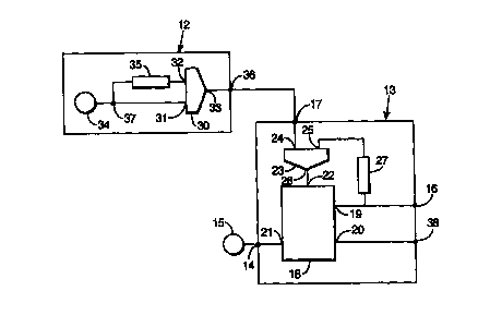
The window generator shown in Figure 2 comprises a
pulse pair generator 12 and a switching device 13. The
switching device 13 has an input port 14, to which is
coupled an pulse stream generator 15, two output ports
16, 38 and a switching input port 17 which is coupled to the
generator output 36 of the pulse pair generator 12.
The switching device itself consists of an all optical
non-linear gate 18 the first gate output 19 of which is
coupled to the second combiner input 25 of an optical
combiner 23, via a feedback loop. The feedback loop is
formed from a delay line 27, which, for the purposes of the
CA 02302237 2000-03-O1
WO 99/14649 PCT/GB98/02731
26
window generator, introduces a time delay equivalent to a
single bit slot. Accordingly, an optical pulse transferred
through the delay line 27 will arrive at the second
combiner input 25 of the optical combiner 23 in the bit
slot immediately following the bit slot it would have
arrived in if it had been travelling through a non-delaying
connection.
The gate input, is coupled to the switching device
input port 14 to receive the optical pulse stream generated
by the pulse stream generator 15, whilst the gate switching
input 22 is coupled to the combiner output 26 of the
optical combiner 23. The first combiner input 24 is
connected to the switching device switching input port 17,
to receive optical pulses from the pulse pair generator 12.
The pulse pair generator 12 consists of an all optical
combiner 30. Connected to a first combiner input 31 of the
optical combiner 30 is a sync pulse generator 34, whilst
connected to the second input 32 is a delay line 35. The
delay line 35, which is also coupled to the sync pulse
generator 34, operates to add a time delay equal to a
number of bit slots N. The combiner output 33 of the
combiner 30, is connected via an output port 36 of the
pulse pair generator 12 to the switching input port 17 of
the switching device 13.
Operation of the window generator will now be
described with reference to Figure 3 which shows bit slot
time lines for several locations around the window
generator circuit. Each time line, which is split into a
series of bit slots, shows the presence of optical pulses
at the respective points in the circuit. A stream of
pulses is represented by the continuous presence of a pulse
although it could equally be shown as a series of discrete
pulses.
As described above, the switching device 13 is coupled
to the pulse stream generator 15 which supplies the optical
pulse stream to the input port 14 of the switching device
and hence to the gate input 21 of the gate 18.
CA 02302237 2000-03-O1
WO 99/14649 PCT/GB98/02731
27
Initially, with no optical pulse applied to the
switching input port 17 of the switching device, there will
be no optical pulse input to the gate switching input 22 of
the gate 18. Accordingly, the stream of optical pulses
supplied to the gate input 21 will pass through the all
optical gate 18 to the gate output 20. As a result, no
optical pulses are output from the gate output 19 and a
stream of pulses are output from the second gate output 20.
In bit slot 5 , as labelled on Figure 3 , the single
optical pulse is output from the sync pulse generator 34
and transferred to the optical combiner 30. As shown in
Figure 3, the single optical pulse arrives at a point 37
and is split into two copies, one of which is transferred
directly to the first combiner input 31 of the all optical
combiner 30, whilst the other is transferred to the second
combiner input 32, via the delay line 35. The pulse
travelling along the delay line 35 will be delayed by N bit
slots (in the present example N=10) with respect to the
pulse travelling directly to the optical combiner 30. As
a consequence, the optical combiner 30 will receive one
optical pulse at the combiner input 31 in the bit slot 5
and a second optical pulse at combiner input 32 in bit slot
15, as shown in Figure 3.
These optical pulses are then combined to form a
single optical pulse stream including two optical pulses
separated by N bit slots, which is transferred to the
switching input port 17 of the switching device 13.
When the first pulse is received from the pulse pair
generator 12, it will be input to the switching input port
17 of the switching device and hence to the first combiner
input 24 of the optical combiner 23, as shown. This
optical pulse is then transferred to the gate switching
input 22 of the gate 18 to act as a switching signal. This
will cause a first optical pulse to be switched from the
gate input 21 to the gate output 19 during bit slot 5.
This optical pulse is fed back via the delay line 27
to the second combiner input 25 of the optical combiner 23.
CA 02302237 2000-03-O1
WO 99/14649 PCT/GB98/02731
28
Because the delay line 27 introduces a single bit delay
into the feedback loop, the fed back optical pulse will
arrive back at the gate switching input 22 in bit slot 6,
as the subsequent optical pulse output from the pulse
stream generator 15 is received at the gate input 21.
Accordingly the first optical pulse output from the gate
output 19 will act as a switching signal, in bit slot 6,
causing the next optical pulse to be switched from the gate
input 21 to the gate output 19. This is repeated for bit
slots 6 to 14, causing a stream of 10 optical pulses to be
output from the gate output 19.
This continues until the second pulse is output from
the pulse pair generator 12, in bit slot 15. This pulse
will arrive at the first combiner input 24 of the optical
combiner 23 in bit slot 15, the same time as an optical
pulse from the feedback loop is received at the second
combiner input 25.
With both pulses arriving at the all optical combiner
23 simultaneously, two optical pulses will be output in the
same bit slot. Accordingly, the gate switching input 22
will detect a total energy equivalent to two optical
pulses. This does not act a switching signal and as a
result, the stream of optical pulses from the pulse stream
generator 15 will no longer be switched to the gate output
19.
Consequently, when placed in combination, the optical
combiner 23 and the gate 18 function as an XOR system, with
the gate 18 only entering the switched state when only one
optical pulse is received at one of the optical combiner
inputs 24, 25. When no pulse is received, or a pulse is
received at both inputs, simultaneously during the same bit
slot period, then the signal output from the combiner will
not act as a switching signal, causing the gate to remain
in an unswitched state.
Thus by providing an optical signal stream from the
pulse pair generator 12 with two pulses, the pulses being
separated by a predetermined number of bit slots N, the
CA 02302237 2000-03-O1
WO 99/14649 PCT/GB98/02731
29
window generator will output an optical signal stream
consisting of N optical pulses, from the gate output 19.
Furthermore, as it is the delay line 35 that
introduces the delay in the pulse pair generator 12, it is
the length of the time delay of the delay line 35 that sets
the number of bits N. Thus in the example of Figure 3, the
delay line 35 introduces a delay equivalent to 10 bit
slots, causing the window generator to output a sequence of
optical pulses from the output port 16. However, the
10 number of bit slots that the delay line 35 delays the
optical pulse by could be altered, causing a corresponding
change in the number of optical pulses output from the
output port 16 of the switching device 13.
It should also be noted that as the second gate output
20 generates an optical signal stream that is the logical
complement of the optical signal stream generated by the
first gate output 19. The second output port 38 is coupled
to the gate output 20 so as to produce an optical signal
stream including an N bit slot window, the N bit slots not
having an optical pulse in. Obviously, with such a stream,
any bit slots not inside the N bit window will include an
optical pulse.
Examples of all optical circuits utilizing the window
generator of the present invention will now be described.
All optical regenerative memories utilizing an all
optical non-linear gate are described in a paper entitled
"All-Optical Regenerative Memory", A. J. Poustie, K. J.
Blow and R. J. Manning, Nonlinear Guided Waves and their
applications, Vol. 15, 1996 OSA Technical Digest Series.
Figure 4 shows a resettable regenerative memory
comprising an L bit regenerative memory 40 connected to the
window comparator of Figure 2.
The memory 4 0 , which has a memory input port 41, a
memory output port 42 and a memory word input port 43,
comprises an all optical non-linear gate 44. The gate
input 45 is connected via the memory input port 41 to the
output port 38 of the switching device 13 of the window
CA 02302237 2000-03-O1
WO 99/14649 PCT/GB98/02731
generator, which generates an optical pulse stream for the
memory 40. The first gate output 46 is connected to the
memory output port 42 and, via a feedback loop with a delay
line 49, to an all optical combiner 50.
5 The all optical combiner 50 has a combiner output 53
connected to the gate switching input 48 of the gate 44,
along with two combiner inputs 51, 52. As in the window
generator of Figure 2, the optical combiner 50 and optical
gate 44 act as an XOR system, the gate only being switched
10 on reception of a bit slot containing a single optical
pulse which acts as a switching signal.
The first combiner input 51 is connected to the memory
word input port 43, for receiving the L bit word to be
stored, whilst the second combiner input 52 is connected to
15 the first gate output port 46, via the delay line 49. The
delay line 49 introduces a time delay equivalent to L bit
slots to the data flow from the gate output to the combiner
input.
Operation of the memory 40 will now be described, with
20 the optical signal stream initially considered as a
continuous stream of optical pulses, with no empty bit
slots.
With no optical pulses applied to the memory word
input 43, the stream of optical pulses supplied to the
25 memory input port 41 will be output from the second gate
output 47 of the gate 44. To store a word, which is data
comprising an optical signal of L bit slots in length, the
word is input to the memory word input 43 and transferred
via the optical combiner 50 to the gate switching input 48.
30 The word acts as a series of switching signals. Thus
as each bit slot of the word is applied to the switching
input, it will cause a copy of contents of the bit slot to
be output from the first gate output 46. So, for example,
if the first bit slot contains an optical pulse, this will
act as a switching signal causing a single optical pulse to
be transferred from the optical pulse stream supplied to
the gate input 45 to the first gate output 46. This
CA 02302237 2000-03-O1
- WO 99/14649 PCT/GB98/02731
31
optical pulse will then be output from the output port 42
with a copy of the pulse being fed back via the delay line
49, to the combiner 50.
As the delay line 49 introduces an L bit slot delay,
this first bit slot containing an optical pulse will not
reach the second combiner input 52 until all the L bit
slots in the word have passed through the combiner 50.
Supposing the second bit slot of the word contains no
optical pulse, then it does not act as a switching signal
and the optical pulse in the corresponding bit slot in the
input optical pulse stream will be transferred to the
second gate output 47. Accordingly an empty bit slot will
be output from the first gate output 46, which will again
be fed back via the delay line to the second combiner input
52.
This process is repeated for all the L bit slots of
the word such that a copy of the word is generated at the
second gate output 46. As mentioned with respect to each
bit slot, the copy of the word is split, with one copy
being available for output from the memory 40 at the memory
output port 42, whilst the other copy is fed back to the
optical combiner 50, via the delay line 49.
As the delay line 49 delays the transfer of the word
by L bit slots, then the first bit slot of the copied word
will reach the input 52 of the optical combiner immediately
after the last bit slot of the word was originally input
into in the input 51 of the combiner 50. This copy of the
word then acts as a further series of switching signals to
generate further copies of the word.
Consequently, a copy of the word constantly
recirculates in the feed back loop acting as a set of
switching signals to cause further copies of the word to be
generated and output from the first gate output 46.
As the memory operates to regenerate the word by
transferring the optical pulses received at the gate input
to the first gate output 46 using the previous copy of
the word to act as switching signals, it is possible to
CA 02302237 2000-03-O1
WO 99/14649 PCT/GB98/02731
32
reset the memory by replacing the input optical pulse
stream received at the memory input port 41, with an
optical pulse stream including a window of at least L bit
slots in which no optical pulses are present . The gate
will then transfer the empty bit slots, to the feedback
loop, thus preventing a further copy of the word and hence
further switching signals being generated.
Such an L bit slot window containing no optical pulses
can be obtained from the window generator of Figure 2, by
connecting the memory input port 41 of the memory 40 to the
output port 38, and ensuring that the N bit slot delay
introduced by the delay line 35 of the pulse pair generator
is greater than, or equal to, L bit slots in length (i.e.
NaL) .
Accordingly, by utilizing the apparatus configuration
shown in Figure 4, in which delay line 35 of the pulse pair
generator introduces an N bit slot delay (for N a L), an L
bit resettable regenerative memory is achievable, the
memory being reset upon the generation of a pulse by the
sync pulse generator 34, which triggers the generation of
the N bit slot window.
Figure 5 shows a resettable word comparator system
utilizing the window generator of Figure 2. The system
includes a window comparator 60 having a comparator input
port 61, first and second comparator word input ports 62,
63 and a comparator output port 64. The comparator 60
comprises an all optical non-linear gate 65, whose second
gate output 68 is coupled to the memory input port 41 of a
1 bit regenerative memory 40'.
The 1 bit regenerative memory 40' functions as for the
L bit regenerative memory 40, described above, except with
the delay line 49' having only a 1 bit slot delay instead
of the L bit slot delay that the delay line 49 has.
Accordingly, the memory 40' is only able to store a word of
1 bit slot in length. This word, which is supplied to the
memory word input 43 by a sync pulse generator 74, is a
single optical pulse which acts as a switching signal
CA 02302237 2000-03-O1
WO 99/14649 PCT/GB98/02731
33
causing a single optical pulse to recirculate in the memory
40' as long as a continuous stream of optical pulses is
applied to the memory input 41.
Coupled to the gate switching input 69 of the gate 65
is an optical combiner 70 whose first and second combiner
inputs 71, 72 are connected to first and second comparator
word input ports 62, 63, of the word cornparator 60,
respectively. The gate input 66 is connected via the
comparator input port 61 to the output port 38 of the
window generator of Figure 1. This generates an optical
signal stream which is transferred via the gate 65 to the
memory input 41 of the memory 40'. The first gate output
67 is left unconnected.
Operation of the word comparator 60 will now be
described, with the optical signal stream initially
considered as a continuous stream of optical pulses, with
no empty bit slots.
The word comparator 60 operates to compare two words
input to the comparator word input ports 62, 63. Each word
is an optical pulse sequence of a specific number of bit
slots M in length, where M is an integer, which represents
a word comprising M bits of data. The words are input to
the comparator word input ports 62, 63 and transferred to
the optical combiner 70.
The optical combiner 70 and the optical gate 65 act as
an XOR system, such that the gate 65 will only enter the
switched state should the two words differ. This arises
due to the combiner 70 adding the two words. If the words
are identical, then for the equivalent bit slots of the
words that contain optical pulses, the optical combiner
will output a double pulse signal, and for the equivalent
bit slots containing no optical pulse, the combiner 70 will
not output any optical pulse . Accordingly, the switch will
not enter the switched state.
However, when the two received words differ, this
means that at some point a bit slot of one word will
contain an optical pulse, whilst the corresponding bit slot
CA 02302237 2000-03-O1
WO 99/14649 PCT/GB98/02731
34
of the second word will not contain an optical pulse. As
a consequence, when combined by the combiner, for the bit
slot that differs, the optical combiner will output a
single optical pulse. This then acts as a switching signal
causing the switch to enter the switched state, resulting
in an optical pulse being output from the first gate output
67. In fact if more bit slots differ between the two
words, then more optical pulses will be output from the
first gate output.
If no switching signal is received at the gate
switching input 69 then the optical pulse stream, received
from the output port 38 of the window generator, is output
from the second gate output 68 to the memory input 41 of
the memory 40'. As this is a continuous stream of optical
pulses then, as described above, a single optical pulse
will constantly recirculate in the memory 40'.
However, if a switching signal is received at the gate
switching input 69 of the gate 65, then a single optical
pulse, from the optical pulse stream will be transferred to
the first gate output 67. Consequently the optical signal
stream output from the second gate output 68 will have an
empty bit slot corresponding to the optical pulse that was
transferred to the first gate output 67.
This empty bit slot is transferred to the memory input
41 of the memory 40' and is transferred to the first gate
output 46 of the gate 44. From here, the empty bit slot
will pass round the feedback loop of the regenerative
memory, back to the gate switching input 48, preventing the
transfer of any further optical pulses received at the gate
input 45. Consequently the memory contents no longer
contain an optical pulse.
Thus, if the memory contents contains an optical
pulse, this indicates that the optical pulse stream output
from the gate output 68 contains no empty slots, indicating
that the two words are identical. Otherwise, if the memory
contents are reset, this indicates the presence of an empty
CA 02302237 2000-03-O1
WO 99/14649 PCT/GB98/02731
slot in the optical signal stream supplied to the memory
input 41, hence indicating a difference in the two words.
However, once the comparator 60 has been initialised
by the pulse from the sync pulse generator 74, it will
5 remain in this state unless two different words are
supplied to the comparator word input ports 62, 63. In
some circumstances it may be necessary to reset the
comparator 60.
This is achieved in a manner similar to the resetting
10 of the L bit regenerative memory described with respect to
Figure 4. Thus, by obtaining the optical signal stream for
the comparator input 61 from the output port 38 of the
window generator, the window generator can be used to
generate signal stream including an N bit slot window where
15 N is of 1 or more bit slots in length. This optical pulse
stream with the N empty bit slots is transferred via the
gate 65 to the memory input 41, causing the memory to reset
as described with reference to Figure 4.
Figure 6a shows in schematic form an all optical
20 packet killer which can be used to remove all optical data
packets from a network system.
In networks that transfer data in packets, it is a
common problem that incorrectly addressed packets continue
to propagate around the network indefinitely. One possible
25 way around this problem is to only use addresses with even
(or odd) parity and then eliminate all packets which have
an address of the opposite parity. Thus, a packet killer
system must be able to detect the address of a data packet,
which is usually stored in the packet header, determine the
30 parity of the address and output the packet from different
outputs depending on the parity.
The apparatus shown in Figure 6a comprises a pulse
pair generator 12 ~ and a switching device 13 which together
form the window generator of Figure 2. This window
35 generator is used to generate a window of Q bit slots in
length, where Q is the number of bit slots used by the
header of the data packet, i.e. the window is equal in
CA 02302237 2000-03-O1
WO 99/14649 PCT/GB98/02731
36
length to the header of the data packet, the total length
of the packet being R bit slots. This is achieved by
ensuring that the delay line 35' of the pulse pair
generator 12' introduces a delay equivalent to Q bit slots,
causing the optical pulses output from the pulse pair
generator 12', to be separated by an Q bit slot interval.
The output port 16 of the switching device 13 is
connected to a gate switching input 101 of an optical gate
100. The gate 100 has a gate input 102 which is connected
to a packet source 300 which is used to input the packets
to the circuit. The second gate output 102 of the gate 101
is unconnected, whilst the first gate output 103 is coupled
to the switching input port 121 of a second switching
device 120.
The second output port 123, of the switching device
120, is unconnected and the first output port 122 is
connected to the gate switching input 107 of an optical
gate 106. The first and second gate outputs 109, 110 are
used to output the packet from the apparatus as either a
rejected or accepted packet, as will be described below.
The gate 106 also has a gate input 108 which is coupled via
a delay line 111 to the packet input 105.
The switching device 120 also has an input port 124
which is connected to the second gate output 116 of an all
optical gate 112. The first gate output is unconnected,
whilst the gate input 114 is coupled to a pulse stream
generator 117 which generates a continuous stream of
optical pulses. The gate 112 has a gate switching input
113 which is coupled via a delay line 118 to the point 37
of the pulse pair generator 12'.
Operation of the packet killer will now be described
with reference to Figure 6b which shows the relative timing
of pulses throughout the circuit for a packet with an even
parity address and then for a packet with an odd parity
address.
The first task of the circuit is to separate the
heavier from the data packet . This is achieved by using the
CA 02302237 2000-03-O1
WO 99/14649 PCT/GB98/02731
37
window generator, comprising the pulse pair generator 12'
and the switching device 13, to generate a window of Q bit
slots in length, Q being the number of bit slots of the
header of the data packet, the data packet being R bit
slots in length. This window is output from the switching
device output port 16 and is shown in Figure 6b as the
pulse train labelled 16.
The Q bit slot window pulse stream is fed to the gate
switching input 101 of the optical gate 100. The data
packets, which are input to the circuit at the packet input
105 are copied to the gate input 102. This is timed such
that the first bit slot in the header of the packet will
arrive at the gate input 101 at substantially the same time
that the first bit slot of the Q bit slot window arrives at
the gate switching input 101. Accordingly, the header of
the data packet is transferred to the first gate output 103
of the gate 100 and transferred to the switching input port
121 of the switching device 120. This is shown by the 121
pulse sequence in Figure 6b. The remaining part of the
data packet, which comprises the packet payload, will
simply be transferred to the second gate output 104, as
shown.
As can be seen from Figure 6b, the header of the first
packet comprises an even number of optical pulses, whereas
the header of the second packet comprises an odd number of
optical pulses. These optical pulses are used as switching
signals to switch the switching device 120.
The source of optical pulses provided to the input
port 124 of the second switching device 120 is provided by
the pulse stream generator 114. The generated pulse stream
is input to the gate 112, which operates to transfer the
optical pulse stream to the regenerative memory via the
second gate output 116. A single optical pulse is applied
to the gate 112 via the delay line 118 from the point 37 in
the pulse pair generator 12'. This is used as a switching
signal, at a later time, to reset the second switching
device 120, as will be described below.
CA 02302237 2000-03-O1
WO 99/14649 PCT/GB9$/02731
38
Assuming for now that a constant optical stream is
supplied to the input port 124 of the switching device 120,
then the switching device 120 is arranged such that an
optical pulse provided to the switching input port 121 acts
as a switching signal, causing the switching device 120 to
change the output optical pulse stream between a continuous
stream of optical pulses and a stream of no optical pulses.
Thus the second switching device 120 function as for the
switching device of Figure 2.
Upon the application of the even parity header to the
switching input port 121, the first pulse will initially
pass through the optical combiner 125 to the gate switching
input 127 of the all optical gate 126. This switching
signal causes a single optical pulse of the optical pulse
stream applied to the input port 124 to be switched to the
first gate output 128. This will circulate in the feedback
loop to return to the gate switching input 127 via the
optical combiner 125. As the delay line 130 introduces a 1
bit slot delay, the pulse will arrive at the optical
combiner 125 at the same time that an empty bit slot
arrives from the switching input port 121.
Consequently, a second switching signal is applied to
the gate switching input 126 causing a second pulse to
circulate through the feedback loop.
Whilst these two optical pulses have been transferred
from the input port 124 to the first gate output 128, the
output port 122 also outputs copies of the two optical
pulses, as shown in the 16 bit slot section of Figure 6b.
However, as the second optical pulse circulating in
the feedback loop reaches the optical combiner 125 a pulse
is also transferred from the switching input port 121. As
a consequence two optical pulses are output from the
optical combiner to the gate switching input 127. As the
switch 126 does not detect the double optical pulse in a
single bit slot as a switching signal, no optical pulse is
transferred to the first gate output 128. Accordingly, an
CA 02302237 2000-03-O1
WO 99/14649 PCT/GB98/02731
39
empty bit slot will be output from the switching device
output port 122.
This is repeated until, as shown in Figure 6b, when
the header has been fully applied to the switching input
port 121 the output port 122 will output a stream of empty
bit slots.
These empty bit slots are applied to the gate
switching input 107 of the gate 106. Supplied to the gate
input I08 is a copy of the packet which is fed via the
delay line 111 from the packet input 105. This delay line
111 applies a time delay to the packet, such that the first
bit slot of the packet arrives at the gate 106 at the same
time as the first bit slot of optical pulse stream output
from the switching device output port 122 i.e. the delay
line 121 applies a Q bit slot delay.
Thus the output from the second switching device 120,
is used to control whether the data packet, including a
copy of the header, is transferred from the gate input 108
to the first gate output 109 or the second gate output 110.
In the case of empty bit slots being applied to the
gate switching input 107, the data will be transferred
directly to the second gate output 110, as shown in Figure
6b.
Operation for a packet with an odd parity address is
identical except that the second switching device 120 will
be left in a state in which a stream of optical pulses are
output from the output port 122 to the gate switching input
107 of the gate 106. These act as switching pulses causing
the data packet to be transferred to the first gate output
109 as shown in the odd parity section of Figure 6b.
In order for the second switching device 122 to
correctly detect the parity of the header address, it is
necessary for there to be no optical pulses in the feedback
loop when the first optical pulse is received at the
switching input~port 121. In order to achieve this, the
optical pulse stream supplied to the input port 124 of the
switching device 120 has an empty bit slot which is timed
CA 02302237 2000-03-O1
WO 99/14649 PCT/GB98/02731
to arrive at the input port 124 at the same time that the
previous data packet has been completely transferred from
the gate input 108 of the gate 106 to one of the gate
outputs 109, 110.
5 The empty bit slot is generated by the application of
a single switching signal to the gate switching input 113,
of the gate 112. The single switching signal is obtained
from the point 37 in the pulse pair generator 12 " and is
delayed by Q+R bit slots by the delay line 118, such that
10 it arrives at the gate 112 at the same time that the header
and packet have been handled by the second switching device
120. The empty bit slot operates to reset the second
switching device 120 by ensuring that should any optical
pulses be recirculating in the second switching device 120,
15 then they will cause the empty bit slot received at the
input port 124 to be switched to the first gate output 128.
As a result, no further optical pulses recirculate in the
feedback loop until further pulses are received at the
switching input port 121.
20 A packet receiver utilizing a window generator
according to the present invention is shown in Figure 7a.
The packet receiver operates to read the address of a data
packet and then determine whether the address is the same
as the address of the receiver itself, and control the flow
25 of the data accordingly.
The data packet itself consists of three sections, a
header, data and a trailing section containing no optical
pulses. Both the header and the trailing section are of S
bit slots in length, whilst the data section is of T bit
30 slots in length.
The packet receiver comprises a pulse pair generator
12 " coupled to a switching device 13 to form the window
generator of Figure 2, with the delay line 35" providing
a S bit slot delay, to cause the window generator to
35 generate an S bit slot window. The switching device output
port 16 is connected to the gate switching input 201 of a
gate 200. The gate input 202 which is connected to a
CA 02302237 2000-03-O1
WO 99/14649 PCT/GB98/02731
41
packet input 205 at which a copy of the packet is received
by the circuit.
The second gate output 204 is unconnected, whilst the
first gate output 203 is supplied to the first word input
port 62 of the word comparator 60 of Figure 4. The second
word input port 63 of the word comparator 60 is connected
to the memory output port 42 of a regenerative memory 40" ,
which functions as for the L bit regenerative memory 40,
described above, except that L bit slot delay line 49 is
replaced by a delay line 49" that introduces a delay
equivalent to S+T+S bit slots (i.e. the entire length of
the data packet).
The memory input port 41 is coupled to a pulse stream
generator 208 which generates a continuous stream of
optical pulses. The memory word input port 43 of the
memory 40" is coupled to an address input 207 which
supplies the address of the receiver circuit. The actual
address is S bit slots long, but has an additional trailing
section, containing no optical pulses, of S+T bit slots in
length, which is added to ensure that the address is only
output from the memory output port 42 once every time a
data packet is received.
A delay line 208 is coupled to the point 37 of the
pulse pair generator 12 " to obtain a single optical pulse
which is used as a switching signal by providing it to the
gate switching input 210 of a gate 209. The gate 209 is
coupled to an pulse stream generator 214 which generates a
continuous stream of optical pulses. The gate 209 has a
first gate output 212 which is unconnected, and a second
gate output 213 coupled to the comparator input port 61 of
the word comparator 60. The comparator output port 64 is
connected to the gate switching input 216 of a gate 215.
The gate input 219 is connected to the packet input 205 via
a delay line 220, for receiving a copy of the packet.
Operation of the packet receiver will now be described
with reference to Figure 7b which shows the presence of
CA 02302237 2000-03-O1
WO 99/14649 PCT/GB98/02731
42
optical pulses at several locations around the packet
receiver of Figure 7a.
Upon initialisation of the packet receiver, the
address of the packet receiver circuit is supplied to the
address input 207 and hence to the memory word input 43 of
the regenerative memory 40" . A copy of this address is
stored in the regenerative memory and repeatedly output
from the memory output 42 to the word input 63 of the word
comparator 60.
The pulse pair generator 12' ' and the switching device
13 generate a header window which is of S bit slots in
length, S being the number of bit slots in the packet
header. The optical pulse stream including the S bit slot
window is output from the switching device output 16, as
shown in Figure 7b, and supplied to the gate switching
input 201 of the gate 200. The data packet itself is
supplied to the gate input 202 such that the first bit slot
of the packet arrives at the same t ime as the first bit
slot of the S bit slot window. The S bit slot window then
acts as S consecutive switching signals causing the header
of the data to be switched to the first gate output 203 and
transferred to the comparator word input port 62 of the
word comparator 60.
As the address stored in memory 40' is equal in length
to the entire data packet, the first bit slot of the
address will arrive at the comparator word input port 63
simultaneously with the first bit slot of the header.
The word comparator then operates as described in
Figure 4 above, to compare the optical pulse streams
received at the comparator word input ports 62, 63. Thus,
the word comparator compares the address of the receiver
circuit with the address indicated in the packet header.
If the addresses are identical, as shown by the CORRECT
ADDRESS set of pulses in Figure 7b, then the word output
port 64 will output a continuous series of optical pulses.
Simultaneously a copy of the data packet is supplied
to the gate input 217 of the gate 215 via the delay line
*rB
CA 02302237 2000-03-O1
- WO 99/14649 PCT/GB98I02731
43
220, which delays the transfer of the packet by S bit
slots, such that the first bit slot of the packet arrives
at the gate input 217 at the same time that the header
address comparison has finished. As the comparator output
port 64 is a stream of optical pulses, due to the compared
words being identical, the optical pulses act as switching
signals so that the data packet received at the gate input
217 is transferred to the first gate output 218, indicating
that the packet has the correct address to be received.
20 The circuit is then reset by the provision of a single
pulse through the delay line 208 to the switching input 210
of the gate 209. This acts to generate an empty bit slot
in the continuous optical pulse stream by transferring a
single optical pulse, from the received continuous pulse
stream, to the first gate output 212. The optical pulse
stream with the single empty bit slot is output from the
gate output 213 to the comparator input port 61 of the word
comparator 60. This resets the word comparator ready for
the next packet to be received.
When the next data packet is received, the circuit is
reinitialised. This involves having the sync pulse
generator 74 generate an optical pulse to ensure that an
optical pulse is circulating in the regenerative memory
40', to allow the circuit to function correctly.
The second packet of data is now received, as shown by
the INCORRECT ADDRESS set of pulses shown in Figure 7b.
For handling the second packet, again a copy of the
address is supplied to the comparator word input port 63 of
the word comparator 60. The second packet is received at
the packet input 205 and as described above, the header is
separated from the packet and transferred to the word
comparator 60. In this case the header is different to the
address and the comparator therefore gives an output which
is a continuous stream of empty bit slots, from the
comparator output port 64.
This continuous stream of empty bit slots is supplied
to the gate switching input 216, a shown in Figure 7b,
CA 02302237 2000-03-O1
WO 99/14649 PCT1GB98102731
44
causing a copy of the packet supplied to the packet input
205 to be transferred to the second gate output 219 of the
gate 215, indicating that the packet is not to be received
by the circuit.
As mentioned above, the data packet comprises a
header, data and a trailing section containing no optical
pulses. The trailing section is required as the packet is
not output from the respective gate output 218, 219 until
the header has been processed. This means that there is a
delay of S bit slots from when the packet is received to
when it reaches one of the gate outputs 218, 219 and as the
packets are received at the packet input 205 immediately
after each other, processing of the subsequent packet
begins before the final S bit slots of the packet have been
output. As this could cause the last S bit slots of data
to be transferred to the wrong gate output, it is essential
to ensure the final S bit slots of the packet are
redundant . This is achieved by incorporating an S bit slot
length trailing section to the packet which contains no
optical pulses.