Note: Descriptions are shown in the official language in which they were submitted.
CA 02304019 2000-03-16
WO 99/15922 PCTNS98119129
Transparent Metallo-dielectric Photonic Band Gap Structure
Background of the Invention
i. Field of the Invention
This invention relates generally to photonic signal devices. In particular,
this invention relates to a transparent metal device that utilizes a photonic
band
gap structure to transmit a selected range of wavelengths of the
electromagnetic
spectrum; such as the visible range, and to reflect all longer wavelengths.
2. Related Art
Recent advances in photonic technology have generated a trend toward the
integration of electronic and photonic devices. In particular, this advance is
due
to the increased desire to utilize and manipulate "photonic signals", as
opposed to
electrical signals, to perform such functions as information transfer. A
"photonic
signal" is a generic characterization of light that includes the entire range
of
electromagnetic frequencies, from gamma to x-rays, from visible Iight to
microwaves, down to radio frequencies and beyond. Photonic devices offer an
1 S array of advantages over conventional electronic devices. For example,
they can
provide enhanced speed of operation, reduced size, robustness to environmental
changes, such as rapid temperature variations, increased lifetime, and the
ability
to handle high repetition rates. These structures can be made of semiconductor
CA 02304019 2000-03-16
WO 99/15922 PCT/US98/191Z9
-2-
materials, ordinary dielectrics, or a combination of semiconductor and
dielectric
materials.
The intense theoretical and experimental investigations of these structures
in recent years, photonic band gap (PBG) structures in particular, are
evidence of
the widely recognized potential that these new materials offer. These optical
devices, whose operating principles are based on a combination of nonlinear
medium response and the physics of the photonic band edge, are extremely
compact in nature (only a few microns in length), and some have electronic
counterparts. It is well understood that a liiedium becomes nonlinear when the
index of refraction of the substance is no longer constant, and is function of
the
applied electromagnetic field.
For example, recent advancements in PBG structures have been made in
the development of a photonic band edge nonlinear optical limiter and switch.
See, "Optical Limiting and Switching of Ultrashort Pulses in Nonlinear
Photonic
Band-Gap Materials", M. Scalora, et al. , Physical Review Letters 73:1368 (
1994)
(incorporated by reference herein in its entirety). Also, advancements in
photonic
technology have been achieved with the development of the nonlinear optical
diode. See, "The Photonic Band-Edge Optical Diode", M. Scalora, et al.,
Journal
of Applied Physics 76:2023 (1994) (incorporated by reference herein in its
entirety). Additionally, a high-gain second harmonic generator based on these
photonic principles has been achieved. See, "Pulsed second harmonic generation
in photonic band gap structures", M. Scalora, et al., to appear in Physical
Review
A, 1997 (incorporated by reference herein in its entirety).
Under ordinary circumstances, however, the medium response need not
be nonlinear in order for the interaction of the electromagnetic waves with
matter
to be useful. For example, the photonic band edge delay line makes use of the
linear properties of the structure to drastically reduce the speed of a light
pulse
propagating through the structure without causing distortion of the pulse or
scattering losses. See, "Ultrashort pulse propagation at the photonic band
edge:
CA 02304019 2000-03-16
WO 99115922 PCTNS98/19129
large tunable group delay and minimal distortion and loss", Physical Review E
54:10788 (1996) (incorporated by reference herein in its entirety).
To use a simple illustration, substances are usually characterized by the
degree to which they conduct electricity. Thus, a distinction can be made
between
good conductors (such as metals), insulators (such as glasses), and
semiconductors (such as gallium arsenide), which under the right conditions
can
display properties common to both metals and insulators. The propagation of
light
inside these substances strongly depends on their conductive properties:
metals
are highly reflective, as well as absorptive, at nearly all light frequencies
of
interest, from long radio waves to short-wavelength ultraviolet (UV) light. On
the
other hand, some dielectric materials may be transparent across the spectrum
(a
slab of window glass, for example).
For this reason, metals are routinely used for radiation shielding purposes,
as in the case of microwave oven cavities, or for their reflective properties,
such
as in conventional household mirrors. On the other hand, dielectric or
semiconductor materials are used in integrated circuit environments, in
waveguides and directional couplers, for example, because they allow the
unimpeded propagation of light beams with minimal losses. Therefore, it would
be highly desirable, under certain circumstances, to have access to a
substance that
can act as a shield (or filter) for a certain range of frequencies such as
microwaves,
and yet be transparent in the visible portion of the spectrum, i.e., a
transparent
metal structure.
Summary of the Invention
The present invention generally relates to a device and method of creating
an optical shield (or filter) based on a transparent metal photonic band gap
(PBG)
structure. In particular, the present invention provides an arrangement of
alternating relatively thin or thick metal layers and refractive material
layers
deposited on an opaque or transparent substrate. This alternating
metal/refractive
CA 02304019 2000-03-16
WO 99/15922 PC"T/US98/19129
-4- -
material layer structure can provide a high degree of suppression of incident
ultraviolet, infrared and microwave radiation, while still providing
substantial
transmission in the visible region ofthe electromagnetic spectrum. By
utilizing a
PBG structure, the shielding device can include thick metal layers to provide
a
S greater degree of isolation of unwanted radiation than for similar metal
layer based
filters that are not designed to take advantage of photonic band gap effects.
According to one embodiment of the present invention, a transparent metal
photonic band gap apparatus is provided to transmit a predetermined magnitude
of visible radiation and to reflect a predetermined magnitude of ultraviolet,
infrared, and microwave radiation. The apparatus includes a transparent
substrate,
a plurality of metal layers, and a plurality of interstitial layers.
A first metal layer is deposited on the transparent substrate. This metal
layer can be any transition metal, preferably silver, aluminum, copper, or
gold.
Subsequent metal layers may be the same metal or different metals than the
first
metal layer. The thickness of the metal layer depends on the user application,
and
can range from approximately 2.5 nanometers (nm) up to 50 nm. Metal layers can
be thicker than 50 nm, depending on the amount of visible transmission
required.
The first interstitial layer is then deposited onto the first metal layer.
Again, the thickness of the interstitial layer depends on the user
application, and
can range from approximately 2. S nm up to several hundred or even thousands
of
nanometers. This interstitial layer can be selected from a group comprising
semiconductor materials, ordinary dielectrics, and a combination of
semiconductor
and dielectric materials.
Subsequent metal and interstitial layers are arranged in a similar,
alternating manner. The subsequent metal layers can be the same or different
metals, depending on fabrication considerations and the desired transmission
properties of the device. Similarly, the interstitial layers can be the same
or
different refractive materials, depending on fabrication considerations and
the
desired transmission properties of the device. This arrangement of
metaUinterstitial layers forms a device that exhibits a photonic band gap
structure.
CA 02304019 2000-03-16
WO 99115922 PCT/US98/19129
By altering the thicknesses of the metal and interstitial layers, the device
changes
its transmission characteristics, such that different ranges and different
magnitudes
of transmission and reflection can be achieved.
According to a second embodiment of the present invention, the
transmission range (in the visible region) of the transparent metal PBG device
can
be altered by applying an external electromagnetic field to the device.
Specifically,
a voltage source can be applied to the interstitial layers of the device to
change
their inherent optical path length. By changing the optical path length of the
interstitial layers, which space apart the metal layers, the photonic band gap
structure of the device is altered. As a result, the visible transmission
range and
magnitude of the device is also altered.
Further features and advantages of the present invention, as well as the
structure and operation of various embodiments of the present invention, are
described in detail below with reference to the accompanying drawings.
Brief Description of the Drawings
The present invention is described with reference to the accompanying
drawings. In the drawings, like reference numbers indicate identical or
functionally similar elements. Additionally, the left-most digits) of a
reference
number identifies the drawing in which the reference number first appears.
FIG. 1 is a schematic diagram of an exemplary photonic band gap (PBG)
structure. The indices of refraction are n, and nz for each consecutive layer,
with
respective widths a and b. Each period is formed by the combination of two
consecutive layers, and has width d = a+b;
FIG. 2 is a transmittance vs. frequency profile for the exemplary PBG
structure shown in FIG. 1;
FIG. 3 is a transmission vs. wavelength profile for a 4-period PBG sample
(solid line), where the silver (Ag) layers are 10 nm thick and the magnesium
CA 02304019 2000-03-16
WO 99/15922 PGT/US98/19129
-6-
fluoride layers are 110 nm thick, and a solid silver film 40 nm thick (dotted
line),
in accordance with an embodiment of the present invention;
FIG. 4 is a transmission vs. wavelength profile for a 20-period PBG sample
(solid line), where the silver layers are 10 nm thick and the magnesium
fluoride
layers are 140 nm thick, and the solid silver film is 200 nrn thick (dotted
line), in
accordance with an embodiment of the present invention;
FIG. 5 is a transmission vs. wavelength profile for a silver/magnesium
fluoride PBG sample (solid line), in accordance with an embodiment of the
present
invention, and the continuous silver film (dotted line), which are both shown
schematically in FIGs. 6A and 6B;
FIG. 6A is a schematic representation of a three-period PBG structure, in
accordance with an embodiment of the present invention, and FIG. 6B is a
schematic representation of a 90 run thick silver film on a substrate;
FIG. 7 is- a transmission vs. frequency profile for a three-period PBG
structure based on a Drude model calculation , in accordance with an
embodiment
of the present invention;
FIG. 8 is a transmission vs. wavelength profile for a nine-period,
silver/magnesium fluoride PBG structure, where the silver layers are 1 Q nm
thick
and the magnesium fluoride layers are 140 nm thick (solid line), and where the
silver layers are 10 nm thick and the magnesium fluoride layers are 250 nm
thick
(dotted line), in accordance with an embodiment of the present invention;
FIG. 9 is the theoretical (solid line) and experimental (dotted line)
transmission vs. wavelength profile for the preferred embodiment of the
present
invention, a 3-silver layer, 2 magnesium fluoride layer, PBG structure;
FIG. 10 is a transmission vs. frequency profile of an example copper plate
at microwave wavelengths; and
FIG.11 is a transmission vs. frequency profile of a preferred PBG sample
at microwave wavelengths, in accordance with an embodiment of the present
invention.
CA 02304019 2000-03-16
WO 99/15922 PCT/US98J19129
_'7_
Detailed Description of the Preferred Embodiments
1. Overview and Discussion of the Invention
The present invention is directed toward a method for developing a
transparent metal device. A transparent metal structure allows the propagation
of visible light, while shielding against all other, possibly harmful
electromagnetic
radiation. The transparent metal device can be tailored to increase the signal
output in the desired transparent frequency range and suppress the intensity
throughput of unwanted radiation. In addition, the transparent window can be
tunable to encompass a different range of frequencies, in the infrared range,
for
example. Further, the methods used to fabricate these devices can be
straightforward. The manner in which this is accomplished is described in
detail
below.
2. An Example Photonic Band Gap (PBG) Structure
Before describing the invention in great detail, it is useful to describe an
1 S example structure in which the present invention can be implemented. The
present
invention provides an apparatus and method to fabricate a transparent metallic
structure that possesses the properties of a transparent glass in the visible
portion
of the electromagnetic spectrum, yet is opaque for all longer wavelengths (or
smaller frequencies) from infrared light to radio waves. T'he transparent
metallo-
dielectric device of the present invention is achieved with the utilization of
a
photonic band gap structure.
A schematic illustration of an example photonic band gap (PBG) structure
102 is shown in FIG. 1. In one dimension, a PBG material is typically composed
of a plurality of layers, whereby such plurality of layers alternates between
a low
and a high index of refraction. Each layer has a fixed index of refraction for
low
power incident photonic signals. For example, a first layer 104 can be chosen
such
CA 02304019 2000-03-16
WO 99/15922 PCT/US98/19129
-g-
that it is a high index layer. Next, a second layer 106 can be chosen to be a
low
index layer. One set of first and second layers is referred to as a period,
such as
period 108.
The widths of the first layer 104 and second layer 106 can also be chosen
such that they are both a fraction of the size of a reference wavelength. For
example, each layer can be one quarter of the reference wavelength. Thus, in
this
example, layer 104 can have a width (or thickness) (a), where a=JL/4n, and
where
~, is the in-air wavelength of an incident photonic signal. Likewise, layer
106 can
have a thickness (b), where b=~l./4n2. This particular structure is referred
to as a
quarter-wave stack. As a consequence ofthis arrangement ofthe dielectric
layers,
light interference effects can cause some wavelengths of light to be
transmitted
through the structure, while another range of wavelengths centered about the
reference wavelength, often referred to as "band gap" wavelengths, are
completely
reflected.
FIG. 2 illustrates the transmissive properties of a similar example PBG
structure. Transmission profile 202 is a plot of the transmission of light as
a
function of frequency from an example quarter-wave stack comprising 20
periods,
or 40 alternating high/low index layers. A transmission of unity 208
corresponds
to 100% of the photonic signal being transmitted. In this example, two
dielectric
materials are chosen. The first layer is a glass, with an index n, = 1.41. The
second layer chosen is air, with an index n2 =1. By adjusting the width of the
first
and second layers, a shift of the location of the band gap to different
wavelengths
is created. This property provides significant flexibility in that a device
can be
designed to reflect a desired range of wavelengths, while providing for the
transmission of other wavelengths.
Thus, a range of wavelengths about some reference wavelength cannot
propagate inside this example device. On the other hand, this example PBG
structure is transparent to other wavelengths, above and below the gap, such
as
gap 210 from FIG. 2. Therefore, it is the absence of those wavelengths from
the
transmitted photonic spectrum that gives rise to the name "band gap." Please
note
CA 02304019 2000-03-16
WO 99/15922 PCT/US98/19129
-9-
that this terminology is analogous to the electronic "band gap" described in
semiconductors, where electrons having a specific range of energies cannot
propagate through a semiconductor region. This analogy, however, is used for
illustrative purposes only.
At wavelengths outside the photonic band gap, i. e., in a range above and
below the band gap, a series of transmission resonances and gaps can be
obtained,
as depicted by transmission profile 202 of FIG. 2: The number of such
resonances
is equal to the number of periods that make up the structure. The width of
these
resonances and gaps is a function of the total number of periods, the indices
n, and
n2, and the difference in index (8n), where 8n= ~ n2-n, ~ , and is known as
the index
modulation depth.
The present invention is described in terms of this example structure.
Description in these terms is provided for convenience only. It is not
intended that
the invention be limited to application in this example structure. In fact,
after
reading the following description, it will become apparent to a person skilled
in the
relevant art how to implement the invention in alternative environments. In
the
drawings, the thicknesses of layers and regions are exaggerated for clarity.
3. Transmission and Reflection Properties of Metallic Structures
Typically, the materials used in the fabrication of PBG structures, or
integrated circuits in general, are either dielectric or semiconductor
substances,
due to their low absorption characteristics. The choice of materials can also
be
dictated by a specific need, material properties, or by available fabrication
techniques. An overriding concern, however, is that the chosen materials
should
not absorb light to any significant extent, so as not to compromise device
operation. For this reason, metallic substances are almost exclusively used to
enhance the reflective properties of dielectric or semiconductor materials.
Enhanced reflective properties are thus achieved by designing and
incorporating
CA 02304019 2000-03-16
WO 99/15922 PCTIUS98/19129
-10-
within a particular dielectric or semiconductor device thick metallic films,
such as
silver, nickel, copper, aluminum or gold.
Theoretical calculations show that the reflectivity of metallic structures can
be enhanced with respect to bulk metal if the metal is arranged to form a
periodic
S structure. For example, a 256 aluminurn/air periodic structure was designed
so
that the reflection from such a structure increased when compared to bulk
aluminum from 96% to approximately 98% for a small range of frequencies. Each
metal film was assumed to be approximately 2.5 nm in thickness. See "Photonic
dispersion surfaces", A.J. Ward, et a1, Journal Physics Condens. Matter 7:2217
( 1995) (incorporated by reference herein in its entirety).
However, the properties of aluminum do not allow the fabrication of
uniform films with such a small thickness (less than 2.5 nm thick). Even if
such
small thickness films could be realized with aluminum or other metals, such a
structure would be opaque to electromagnetic waves of all wavelengths, as
calculations show. Therefore, it is desirable to utilize thicker metal layers
in a
PBCr structure for a variety of applications.
According to the present invention, a photonic device based on a PBG
structure comprising thick or thin metal layers is provided. This transparent
metal
PBG device propagates light through these metal films and renders these
structure
transparent to visible light. This phenomenon is best explained through
focusing
specifically on the transmissive properties of PBG structures.
Structures that contain at most two silver layers, each about I O-15 nm in
thickness, sandwiched between silver nitride layers, have been described. See,
e.g., U.S. Patent No. 5,557,462, to Hartig et al and U.S. Patent No. 4,179,181
to
Chang (each incorporated by reference herein in its entirety). However, these
conventional structures still allow anywhere from 5% to 50% transmission of
light
energy in the infrared (IR) wavelength range and as much as 20% of near UV
radiation (320-400nm). For example, screening IR light from the sun
corresponds
to reflecting wavelengths between 750 and 2500 nm, where most of the infrared
solar emission is found. See, University Astronomy, J.M. Pasackoff and M.L.
CA 02304019 2000-03-16
WO 99/15922 PCTIUS98/19129
-11-
Kutner, W.D. Saunders Company, 1978, especially Chapter 8 (incorporated by
reference herein). Consequently, since heat energy is reflected, any enclosed
environment will tend to remain cooler longer than usual, even if exposure to
sunlight persists. Hence, the present invention can be incorporated into
coating
processes designed to significantly lower cooling costs.
Additionally, tunable transmission bands with transmissive and reflective
properties that resemble those of a good metal shields are desirable for a
wide
range of frequencies. According to the present invention, these types of
transmission bands can be generated in structures comprising more than two
silver
layers. The conventional thought in this area, however, is that either an
increase
in thickness, or the presence of additional metal layers, can drastically
reduce the
transmission of visible light.
According to the present invention, the transmission of light at visible
wavelengths does not change appreciably, and can be controlled effectively
with
a metallo-dielectric, periodic structure comprising more than two silver
layers.
Further, the reflective properties of the resulting transparent metal PBG
structure
can be as good as those found in metal shields forvery low frequency (VLF,1000
to 15000 Hz) and extremely low frequency (ELF, zero to 1000 Hz) radiation,
present near high-power lines, and to some extent, near appliances and
television
sets.
It is well understood that light can actually propagate a small distance
inside metals before it is mostly reflected. A small amount of light, on the
order
of 1 % or less, is absorbed, and reappears as heat given off by the metal.
This
characteristic length depends on the wavelength of the incident light, and it
is
referred to as "skin depth". The "skin depth" is arbitrarily defined as the
distance
at which the value of the field has decreased to approximately 37% of the
field
value at the input surface of the metal. See Classical Electromagnetic
Radiation,
by J. B. Marion, Academic Press, 1965 (incorporated by reference herein in its
entirety).
CA 02304019 2000-03-16
WO 99/15922 PCTNS98/19129
-12-
For example, the skin depth of metals such as aluminum, silver, or gold is
between 4 and 10 nm at visible wavelengths (where the wavelengths of visible
light comprise the range of approximately 400-700 nm). On the other hand, the
skin depth for a typical metal at microwave wavelengths can be tens of microns
(typical microwave wavelengths can be on the order of centimeters and meters).
This implies that externally incident waves will propagate approximately these
respective distances inside the metal, depending on the incident wavelength,
before
being substantially reflected. Therefore, a metal film whose thickness is in
excess
of 10 or 15 nm is usually considered a thick film for visible light, while
extremely
thin for microwave radiation and radio waves:
The term "skin depth" described above is a useful concept as long as light
is incident on uniform, highly reflective metal films that are more than I
micron
(pm) thick. However, the term "skin depth" loses its conventional meaning in
the
case of a periodic structure, where the presence of closely spaced boundaries,
i. e. ,
spatial discontinuities of the index of refraction, alters the physical
properties of
the structure as a whole. Some of these properties include modification of the
effective speed of light, suppression of absorption, and transmission and
reflection
coefficients.
4. Transparent Metal PBG Structures
The present invention is based on metallic PBG structures. In the
preferred embodiment, a PBG device includes a plurality of alternating
material
layers. The first material component is a transition metal. For example, this
metal
can be gold, silver, copper, aluminum, tungsten, bismuth, or in general a good
conductor of electricity with properties similar to those of gold, silver,
copper, etc.
~ The second material component is a dielectric or semiconductor material. For
example, glasses such as quartz or magnesium fluoride (MgF2) can be used, and
semiconductors such as gallium arsenide, aluminum arsenide, or germanium can
also be used. Further, any alloy or other material that can be combined with a
CA 02304019 2000-03-16
WO 99/15922 PCTNS98/19129
-13-
metallic substance can also be engineered and used for this purpose. This
combination of materials results in a new index of refraction and new
absorption
characteristics for the PBG structure. These properties can depend on the
respective proportions of the materials used in the structure. It should be
noted,
however, that similar structures that use different metals can respond to the
same
photonic signal in very different ways. Also, the ordering of the
metal/dielectric
structure can be interchanged to a dielectric/metal structure without
affecting the
transmissive properties of the PBG structure.
As an example to illustrate the preferred embodiment of the present
I O invention and its operation, a transparent metal PBG structure can be
fabricated
with the component layers of silver (Ag), a metal, and magnesium fluoride
(MgF2),
a glass. Here, the total amount of Ag in the transparent metal PBG device can
be
hundreds of skin depths in thickness. Similarly, the thickness of the MgF2
layers
can also vary.
In particular, the transparent metal shielding device is a PBG structure
comprising several altennating Ag/MgF2 layers deposited on a glass, or any
other
suitable substrate. For some applications, it can be desirable that the
transmitted
range of frequencies not be in the visible range. Thus, the substrate can be
opaque
to visible light. For example, semiconductor substrates such as aluminum
arsenide
(AIAs) and gallium arsenide (GaAs) can also be used as a substrate, depending
on
what transmission window is desired.
Calculations to determine the theoretical transmission properties of the
device can be performed using matrix transfer method and beam propagation
method mathematical models. See, e.g., Modern Optics, by G.R. Fowles, Dover
Publications, second edition (1975), and "A Beam Propagation Method that
Handles Reflections", M. Scalora and M.E. Crenshaw, Optics Communications
108:191 (1994) (each incorporated by reference herein in its entirety).
The theoretical transmission properties of such a Ag/MgF~ structure can
be calculated as a function of wavelength (or frequency), as a function of the
number of layers and/or layer thickness, and the incident angle of the input
light
CA 02304019 2000-03-16
WO 99/15922 PCTNS98/19129
-14-
beam. For purposes of the present invention, calculations were performed
assuming an example glass substrate, whose index of refraction is
approximately
1.5 for a wide range of incident wavelengths. It is well understood that the
index
of refraction of nearly all substances depends on the wavelength of the
incident
light. This physical principle is referred to as material dispersion, which
can vary
from substance to substance. For purposes of the present invention, the
substrate
functions to hold the metaUdielectric layers in place, and its exact physical
properties can vary (i.e., the substrate need not always be transparent).
According to the present invention, a transparent metal PBG device can
comprise a plurality of metal layers as thin as 10 nm (or thinner, as long as
the
properties of the layer are smooth and uniform throughout) and as thick as 50
nm
or greater. These thickness values are intended as practical illustrations and
are
not intended to limit the present invention. In practice, this lower limit
depends
on available techniques that allow the metal film to be uniformly deposited on
a
substrate. The upper limit of the individual layer thickness can be dictated
by a
specific need. While 50 nm appears to be a reasonable upper limit in terms of
most applications, some applications, such as arc welding, can require a metal
layer thickness of greater than 100 nm.
The present invention allows a user to determine a transmission profile
based on a total metal thickness. A user can slice this total metal thickness
into
any number of individual metal layers in order to achieve the desired
transmission
window. For example, calculations show that a single Ag layer 40 nm in
thickness
suspended in air transmits 2.5% of the incident red light, 8% of green light,
and
about 15% of blue light. This transmission profile is illustrated in FIG. 3,
dotted
line 302. Thus, this example film is essentially opaque to visible light.
However,
if the original 40 nm Ag film is sliced into four Ag layers, each
approximately 10
nm in thickness and spaced apart by approximately 110 nm thick MgF2layers,
then
the total transmission of visible light (400-700 nm) increases to an average
of
70%. This is shown in the solid line 304 of FIG. 3. w
CA 02304019 2000-03-16
WO 99/15922 PCT/US98I19129
-15- - -
According to another example, a 200 nm thick Ag film is completely
opaque to nearly all frequencies, allowing only 10'' of the incident visible
light to
be transmitted. This is shown in FIG. 4, dotted line 402. On the other hand,
if the
original Ag film is sliced into 20 layers, each approximately 10 nm thick, and
spaced apart by approximately 140 nm thick MgFz layers, then the average
transmission in the visible range of frequencies increases to about 35%. This
is
shown in FIG. 4, solid line 404. The significant improvement in transmission
for
the multiple Ag/MgF2 layer PBG structure is approximately seven orders of
magnitude greater than for the single 200 nm Ag film structure. At the same
time,
the periodicity of the multiple Ag/MgFz layer structure described above also
ensures better suppression of the transmitted light in the ultraviolet (UV)
wavelength range (200-400 nm).
Generally speaking, adding more Ag/MgF2 periods to the PBG structure
causes a decrease in the transmitted light intensity. In addition; adding more
Ag/MgF2 periods can suppress the transmission of all lower frequencies and a
good portion of the UV range. For example, a 40-period Ag/MgFz structure,
where each Ag layer is 10 nm thick and each MgF2 layer is approximately 200 nm
thick, causes the average transmission of the device in the visible range to
decrease
to approximately 10%. At the same time, the transmission at all lower
frequencies
beginning in the near infrared (NIR) (at approximately 800 nm) is reduced to
levels well below 10'x° . This value represents an extremely high
degree of
isolation, with essentially zero transmission in the NIR. Please note that
reducing
the. number of periods to 20, and doubling the thickness of the Ag layers to
approximately 20 nm each yields approximately the same results. Furthermore,
even fewer, but thicker Ag layers can be used to achieve approximately the
same
effect, thus adding flexibility to the design of a device for a specific
purpose. As
described in detail below, PBG structures can be fabricated that contain three
periods, but where the metal layer thickness is approximately 30 nm. As is
shown
in FIG. 3, at visible wavelengths, a 30 nm thickness is considered a very
thick
metal film. Therefore, it would be ordinarily considered counterintuitive to
add
CA 02304019 2000-03-16
WO 99/15922 PCT/US98/19129
-16-
even more metal layers in order to improve the transmissive properties of the
resulting structure.
FIG. 5 displays two transmission profiles. The solid line 502 represents
the results of a theoretical calculation for the transmission of light as a
function of
incident wavelength from a PBG structure that comprises a glass substrate and
a
three period, Ag/MgF2 PBG structure. Each Ag layer is approximately 30 nm
thick, and each MgF2 layer is approximately 150 nm in thickness. A schematic
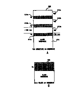
representation of this transparent metal PBG structure in shown FIG. 6A.
As a comparison, the transmission from a single layer, solid 90 nm Ag film
is shown as the dotted line 504 in FIG. 5. A schematic representation of this
PBG
structure 650 in shown FIG. 6B. Thus, PBG structure 650 comprises the same
total amount of silver as in the PBG structure 602 from FIG. 6A.
Further, FIG. S shows that the transmission from the solid metal film
(dotted line 504) is approximately 10-3 in the visible range of wavelengths
{from
400 to 700 nm). This transmission value is equivalent to approximately 30
decibels (dBs) of suppression in the transmitted light (where a factor of 10
change
in transmission is equivalent to 10 dB of isolation). On the other hand, the
maximum transmission (region 510) from solid line 502 (of the periodic PBG
structure 602) is nearly 50% of the incident radiation, or four orders of
magnitude
greater compared to the solid Ag film 650. This maximum transmission is
characterized by a peak in the green region (around 520 nm). Overall, this
maximum transnvssive range 510 extends over a substantial portion of the
visible
wavelength region.
A further transmission resonance 512 appears at approximately 320 nm,
in the ultraviolet (UV) wavelength range. This UV transmission peak 512,
however, is not due to the periodicity of the PBG structure 602, since it can
be
identified for both samples 602 and 650. The UV transmission peak 512 results
from an inherent property of Ag, which becomes slightly transparent to UV
radiation. This characteristic transparency disappears in either case, if the
thickness of the metal film is further increased. For example, the ultraviolet
CA 02304019 2000-03-16
WO 99/15922 PCTNS98/191.29
-17-
transparency region is not present when gold and/or copper are used in a PBG
structure, such as PBG structure 602, described above.
At longer wavelengths (region 520) beyond the visible range, the
calculated transmission of light from the PBG structure is approximately 10's
of
its incident values, or 50 dBs of isolation. This behavior persists in the
limit of
infinite wavelength, or zero frequency.
FIG. 7 displays the results of a calculation of the transmission versus
frequency for the metal PBG structure 602 modeled using the dielectric
constant
derived from a Drude model calculation. See Classical Electromagnetic
Radiation, by J. B. Marion, Academic Press, 1965. Briefly, the Drude model is
an extension of the classical theory of electrons for metals. It provides an
accurate
theoretical representation of the dielectric constant (or index of refraction
and
absorption characteristics) for most metals, including silver, for a range
that
includes low-frequency radio waves and high-frequency ultraviolet light.
FIG. 7 shows that the transmission of light is suppressed for all frequencies
710 and 712 up to the visible range 714, where a maximum of approximately 50%
is transmitted through the PBG device 602. In addition, a band gap
characterizes
a good portion of the UV frequency range 716, which as a result is also
suppressed, as shown in FIG. 7. The small-frequency range depicted in FIG. 7
includes all communication frequency bands, microwave, and IR light. The
calculation represented by FIG. 7 also suggests that in the limit of zero-
frequency,
i. e., ELF and VLF radiation, the transmission is suppressed down to levels
better
than 1 part in 10,000 of the incident photonic signal intensity values.
Therefore,
FIG. 7 represent the theoretical realization of what is referred to as a
"transparent
metal structure": it is transparent in the visible range, it functions as a
good metal
reflector at lower frequencies, and it suppresses UV light to a substantial
degree.
This preferred embodiment of a transparent metal PBG structure, such as
PBG structure 602, can also be fabricated using alternative material layers.
Additionally, many different metals and dielectric or semiconductor
thicknesses
, can be used as well. For example, by keeping the total silver thickness
constant
CA 02304019 2000-03-16
WO 99/15922 PCT/US98/19129
-18-
at about 90 nm, the transmission through the transparent metal structure can
improve to an average of 60% with a total of eighteen layers; i.e., nine metal
layers each 10 nm in thickness, and nine MgF2 layers each 140 nm in thickness.
This improvement in transmission suggests that by modifying each metal layer
and
each MgF2 layer independently, the transmission can be even further optimized.
FIG. 8 (solid line 802) is a representation of the transmission for the
eighteen layer structure described above. In addition to controlling the
magnitude
of suppression of certain wavelengths of light, the present invention also
provides
for the control of the wavelength range where light is transmitted. This
wavelength range control is accolriplished by either increasing or decreasing
the
thickness of the MgF2 layers, and by altering the thickness of the metal
layers to
a lesser degree. For example, FIG. 8 shows an example of this change in
transmission profile. Solid line 802 represents an eighteen layer structure,
where
each Ag layer is 10 nm thick, and each MgF2 layer is 140 nm thick. Dotted line
804 represents the transmission of a similar eighteen layer, where each Ag is
10
nm thick, but where each MgF2 layer is approximately 250 nm in thickness.
Thus,
as illustrated in FIG. 8, more uniform transmission in the visible range can
be
achieved when one of the higher order pass bands is tuned to the visible
wavelength range. The desired transmission profile is accomplished by
utilizing
thicker interstitial (dielectric or semiconductor) layers. These transmission
profiles
802 and 804 help illustrate the flexibility of the present invention.
According to the present invention, the thicknesses of either the metal
layers or the dielectric (or semiconductor) layers can be chosen dependant
upon
the specific application. Cost can also be a driving factor in PBG device
design.
Transparent,, metal PBG devices with fewer periods are generally cheaper to
manufacture, while the thickness of very thin metal films are more difficult
to
control. Further embodiments of the present invention can use a combination of
two or more metals, and/or two or more types of dielectric or semiconductor
materials within the same PBG structure; without any significant departure
from
the basic characteristics already described.
CA 02304019 2000-03-16
WO 99115922 PCT/US98/19129
-19-
Thus, the present invention demonstrates that light can be transmitted
through thin or thick, periodic, metallic structures. Additionally, the
thickness of
the dielectric or semiconductor sandwiched between the metal films can be
controlled, as well as the thickness of each metal film, in order to tune the
transparency regions of the transparent metal PBG device. Just as
significantly,
while the transparent metal PBG device exhibits a transparency window in the '
visible range of frequencies, all lower frequencies (or longer wavelengths),
as well
as a substantial portion of the UV range, are rejected by a substantial
amount.
Further, the present invention encompasses several different methods of
providing a tunable transparency window (or pass band). As mentioned above,
controlling the wavelength range where light is transmitted can be
accomplished
by increasing or decreasing the thickness of the interstitial MgF2 layers.
Other
methods of tuning the transparency window include adding more periods to the
structure and applying an external electric field to the transparent metal PBG
device. These tuning methods are described in detail below.
According to another embodiment of the present invention, it is possible
to use dielectric or semiconductor materials as interstitial layers sandwiched
between the metal layers such that their index of refraction is a sensitive
function
of an externally applied field. Modification of the index of refraction is
equivalent
to adjusting the optical path length of the layer. Therefore, the transparent
wavelength range can be tuned (or moved on the wavelength axis) with the
application of a static field, as for example, in the electro-optic effect.
Further, the transparent window can be changed dynamically by a time-
varying field that propagates through the transparent metal PBG structure for
applications to optical limiting, switching, and optical diode behavior. For
example, increasing the input intensity can cause increased reflections and
drastically reduced transmission in the case of an optical limiter, and
unidirectional
propagation in the case of an optical diode.
CA 02304019 2000-03-16
WO 99115922 PCT/US98/19129
-20-
S. Experimental Results oja Transparent Metal PBG Photonic Device
Recall that FIG. 6A shows a schematic representation of a device 602 that
is referred to as a "transparent metal PBG structure" according to the present
invention. The transparent metal PBG device 602 receives a photonic signal of
wavelength ~.. The photonic signal is partially transmitted by the transparent
metal
PBG device 602 only if the wavelength ~, is found within the ranges outside of
the
photonic band gaps, such as those depicted in FIG. 8 (described above).
Also recall that the transparent metal PBG device 602 of FIG. 6A is a PBG
structure that includes a plurality of first and second alternating layers
(also
referred to as a multilayer stack). The layers alternate between silver layers
61 Oa-
610c, whose index of refraction has value n2 that is a function of wavelength,
and
MgF2 glass layers 612a-612c, whose index of refraction has value n,, which is
also
a function of wavelength.
For example, a transparent metal PBG device similar to the device 602,
from FIG. 6A described above, was fabricated and tested. The experimental
device
comprises: ( 1 ) a rectangular glass substrate (similar to substrate 614),
about Scm
long and 2.5 cm wide; (2) three Ag layers (similar to layers 610a-610c), each
approximately 27.5 nm in thickness; and (3) two MgF2 layers (similar to layers
612a-612b) each approximately 156 nm thick, in the order,
Substrate/Ag/MgF2/Ag/MgF~/Ag.
The first Ag layer 610a was deposited by conventional vacuum
evaporation techniques on substrate 614. In this example, a glass substrate
614
was used, whose index of refraction is 1.51. However, any other suitable
substrates (such as plastics or other materials) can be used without affecting
the
fundamental transmission and reflection properties of the transparent metal
PBG
device 602. In addition, the experimental device was designed so that its
transmission would be a maximum at green wavelengths (around 520 nm).
The second layer, MgFZ layer 612a, was grown by conventional vacuum
evaporation techniques on the first Ag layer 610a. The Ag and MgF2 vacuum
CA 02304019 2000-03-16
WO 99/15922 PCT/US98/19129
-21- - -
evaporation processes were repeated to add subsequent layers. For simplicity,
the
third and final MgF2 layer 612c was omitted without affecting the overall
properties of the transparent metal PBG device 602.
Moreover, a three-period structure was chosen as a preferred embodiment
of the present invention because with fewer than three periods (or in this
case,
fewer than three metal layers) the band structure of the device is not well
defined.
For example, calculations were performed on a structure utilizing only two
metal
layers (i.e., a two period structure). Each metal layer can be greater than SO
nm
thick in the two period structure, which still provides approximately 10 to 15
percent transmission in the visible range (i. e. , less than 1 dB of
suppression). This
transmission magnitude is similar to what is found in conventional, tinted car
windows. However, the resonance peaks created in the photonic band gap
structure are not very broad. Calculations similar to those described above
show
that the band structure becomes well defined once a rudimentary periodicity
(i. e. ,
greater than two periods) is built into the PBG device. Additionally, the
bandwidth of the pass band (i. e., the transparency region) tends to increase
with
the number of periods in the PBG device. Thus, while the two period structure
can operate as a filter, according to the present invention, it is preferred
to utilize
more periods in order to control the transmission characteristics of PBG
device.
The calculated theoretical transmission for this transparent metal PBG
device 602 is shown in FIG. 9, solid line 902. Dotted line 904 represents the
actual transmission for the experimental transparent metal PBG device 602, and
is described further below.
The structure of transparent metal PBG device 602 can be modified to
include thicker MgF2 layers. For example, increasing the thickness of each
inner
MgFz layer to 200 nm causes the band structure of curves 902 and 904 of FIG. 9
to shift up in wavelength, in analogy to the example discussed in connection
with
FIG. 8. In addition, the maximum transmission can be further increased by at
least
10% by adding a third and final MgF2 layer 612c, with a thickness of 100 nm
instead of 200 nm. Therefore, the overall transmission can be enhanced by
CA 02304019 2000-03-16
WO 99/15922 PCTIUS98/19129
-22- -
changing the thickness of the individual layers comprising the transparent
metal
PBG device.
After the experimental transparent metal PBG device was fabricated, two
tests were conducted. In the first test, photonic signals of wavelengths in
the
range between 300 and 900 nm were delivered to the transparent metal PBG
device. The results of this experiment are shown in FIG. 9, dotted line 904.
Some
small disagreements between theory (solid line 902) and experiment (dotted
line
904) can be identified in FIG. 9. However, this minor discrepancy is due to
the
uncertainty in material layer thickness that occurs in the evaporation
chamber.
Overall, the agreement between theory (solid line 902) and experiment (dotted
line
904) is nevertheless extremely good. In this case, the error is approximately
1 to
5 percent. However, this error value is inherently due to the vacuum
deposition
process used to grow the PBG structure. This error can be reduced by refining
the deposition technique (e.g., using an ion sputtering deposition technique).
A second test was conducted to verify that the experimental transparent
metal PBG device was also a good reflector of microwave radiation, as
predicted
in FIG. 7. The second test employed a microwave transmitter and receiver that
operated in the range 2 to 20 GHz (or 109 Hz), which is a regime where the
photonic signal wavelength varies from approximately 1 to 15 centimeters (cm).
In particular, this test was conducted to compare the shielding abilities of a
standard copper metal plate several millimeters in thickness with the
experimental
device. This comparison is shown in FIGs. 10 and 11.
FIG. 10, signal 1002 shows the microwave response of the standard
copper shield by plotting transmission versus frequency. Along the y-axis,
each
separation is equivalent to a drop of 10 dBs. The signal 1002 at the receiver
is
suppressed between 30 and 40 dBs with respect to free space reception for the
range 2-20 GHz, which is indicated by the thick, horizontal line 1004.
Similarly, in FIG. 11, signal 1102 represents the microwave performance
ofthe experimental transparent metal PBG device. Again, the free space
reception
for the range 2-20 GHz is indicated by the thick, horizontal line 1104. These
CA 02304019 2000-03-16
WO 99115922 PC"f/US98/19129
-23- - -
results are in excellent agreement with the theoretical predictions presented
in
FIG. 7. Comparing FIGs. 10 and 11 illustrates that the suppression by the
experimental PBG device at the receiver is at least as good as the metallic
copper
plate. Thus, this comparison verifies that the experimental PBG device is
indeed
a "transparent metal structure."
6 Applications of the Present Invention
The following discussion is by way of example and is not intended to be
a limitation of the possible applications of the present invention. As
described
above, the present invention provides for a device and a method of fabricating
a
transparent metal structure that allows the propagation of visible light,
while
shielding against all other, possibly harmful electromagnetic radiation. The
transparent metal device provides a potential user a great deal of flexibility
in that
the transparent metal PBG device can be tailored to increase the signal output
in
the desired transparent frequency range and suppress the intensity throughput
of
unwanted radiation. As a result, very broad shielding performance, coupled
with
high attenuation of unwanted radiation, can be achieved by the present
invention
through the use of a PBG structure.
This broad shielding capability (one that can encompass the wavelength
regions on both sides of the visible region of the electromagnetic spectrum)
has
a wide range of commercial, industrial, and scientific applications. For
example,
the present invention can operate to shield (or filter) radiation at very low
frequencies (VLF) and extremely low frequencies (ELF). Thus, the transparent
metal PBG techniques described above can be utilized in designing filter or
shield
coatings for television screens and monitors, as well as for cathode ray
tubes,
thereby enhancing the display capabilities ofthese devices. The present
invention
allows for sufficient transmission of visible radiation, while blocking VLF,
ELF,
and ultraviolet (UV) emissions from these display devices. Additionally, the
present invention can be used to coat waveguides to reduce losses.
CA 02304019 2000-03-16
WO 99/15922 PGT/US98/19129
-24-
Moreover, the present invention can be used in place of indium Tin Oxide
for applications requiring a transparent conductor. For example, these
applications include touch panel displays, liquid crystal displays, and liquid
crystal
windows.
Another application for the present invention, provides human eye
protection in the form of sun glasses (to block UV light), laser safety
glasses or
goggles (which can attenuate harmful UV, visible, and IR radiation from Class
N
laser sources), and arc-welding shields. Additionally, the transparent metal
PBG
structure can be incorporated into an optical coating that can be used, for
example, to coat optics mirrors arid windows (to transmit some wavelengths of
interest and reflect other wavelength ranges), to protect paintings that are
susceptible to UV radiation, or to coat compact disks (to prevent the aging
effects
due to prolonged sunlight exposure).
A further application for the present invention provides a method of
fabricating tliemial windows, which block IR radiation completely, while
achieving
good transparency levels in the visible spectrum. As shown above, IR
transmission levels can be attenuated down to below 10'', while still
providing at
least SO% transmission or better in the visible. Commercially, the present
invention can be used, for example, in automotive glass coating techniques to
provide a cooler automobile interior even under conditions of continued
exposure
to sunlight, leading to lower cooling costs.
Additionally, the present invention can be used in a variety of microwave
applications. For example, microwave oven windows can be coated according to
the present invention in order to confine microwave radiation inside the
cavity
while still allowing substantial visibility through the window.
Another application of the present invention involves sensor protection and
packaging. Screening an electronic circuit according to the transparent metal
PBG
techniques described above can lead to a decrease in the weight of shielding
material. For example, in space applications, weight reduction is crucial due
to
launch payload restrictions.
CA 02304019 2000-03-16
WO 99!15922 PCT/US98I19129
-25-
Further, the present invention provides for efficient electromagnetic
signature reduction. For example, a transparent metal PBG shield does not
allow
any frequency that would represent noise from escaping an electronic device
cavity, thus lowering the probability of interception of electronic signals
generated
by the electronic device. The advantage of the present invention provides for
signature reduction, while still allowing a user to see through the shielding
device.
The transparent metal PBG structure can also be used as a conductive element
in
an electronic circuit.
In addition, the present invention provides a technique for fabricating a
decorative transparent window, whose tint changes with the time of day: The
transmitted color depends on the angle at which sunlight is incident on the
window.
7 Conclusion
While various embodiments of the present invention have been described
above, it should be understood that they have been presented by way of example
only, and not limitation. Thus, the breadth and scope of the present invention
should not be limited by any of the above-described exemplary embodiments, but
should be defined only in accordance with the following claims and their
equivalents. Additionally, all articles and patent documents mentioned above
are
incorporated by reference herein.