Note: Descriptions are shown in the official language in which they were submitted.
CA 02304045 2000-03-15
P(',T/AU98/00.778
Received 14 April 1999
ELECTRON DEVICES FOR SINGLE ELECTRON
AND NUCLEAR SPIN MEASUREMENT
Technical Field
Electrons and some nuclei possess a quantized unit of angular
momentum called "spin". This invention concerns electron devices for
single electron and nuclear spin measurement.
The ~ 1'.L) notation is used here to represent the electron spin
state, and the ~ 01) notation the nuclear state. For simplicity, normalization
constants are omitted.
In two electron systems, the electron spins may be aligned (total spin
angular momentum =1) in triplet states ( ~ ~..~) , ~ TT) , and ~ T.~+~.1')) or
opposed (total spin angular momentum=0) in a singlet state ( ~T.~-~.T)).
Similarly the nuclear spins may be aligned or opposed. In the ~~.~~11) state,
all spins point in the same direction.
Background Art
In the laboratory, large numbers (=1023) of electron and nuclear spins
are regularly probed using traditional magnetic resonance techniques.
There are important applications for devices and techniques that can
measure a single electron or nuclear spin. For example, magnetic resonance
experiments could be performed on a single atom or molecule and the local
environment (electric and magnetic fields) could be measured with great
precision. Alternatively, single electron or nuclear spins could be used as
qubits in a quantum computer. Single spin measuring devices would be
required in the computer to initialize and to measure the single-spin qubits.
Summary of the Invention
A first aspect of the invention is an electron device for single spin
measurement, comprising:
A semiconductor substrate into which at least one donor atom is
introduced to produce a donor nuclear spin electron system having large
electron wave functions at the nucleus of the donor atom.
An insulating layer above the substrate.
A first conducting gate on the insulating layer above the donor atom
to control the energy of the bound electron state at the donor.
AMENDED SHEET (Article 341 l>PEA/Ain
CA 02304045 2000-03-15
WO 99/14614 PCT/AU98/00778
2
A second conducting gate on the insulating layer adjacent the first
gate to generate at least one electron in the substrate.
In use, a single electron is bound to the donor, and the donor atom is
weakly coupled to the at least one electron in the substrate. The gates are
biased so that the at least one electron in the substrate will move to the
donor, but only if the spins of the at least one electron and the donor are in
a
relationship which permits the movement.
The arrangement is such that detection of current flow, or even
movement of a single electron, in the device constitutes a measurement of a
single spin.
The motion of a single electron may be detected by probing the
system capacitively, for instance by using single electron capacitance
probes, and any metallic lead can couple to the system, with no special
requirement for spin-polarized electrons. Alternatively, the charge motion
may be detected by single electron tunnelling transistor capacitance
electrnmetry.
A first example of the invention is an electron device for single
electron spin measurement, comprising:
A semiconductor substrate into which at least one donor atom is
introduced to produce a donor nuclear spin electron system having large
electron wave functions at the nucleus of the donor atom.
An insulating layer above the substrate.
A conducting A-gate on the insulating layer above the donor atom to
control the energy of the bound electron state at the donor.
A conducting E-gate on the insulating layer on either side of the A
gate to generate a reservoir of spin polarised electrons at the interface
between the substrate and the insulating layer.
In use the donor atom is weakly coupled to the two reservoirs of
spin-polarized electrons, both reservoirs have the same polarisation, and a
single electron, whose spin is to be determined, is bound to the donor. The
E-gates are biased so that current will flow between them, but only if the
spin on the donor is opposite to the spin polarization in the reservoirs. In
this case one electron at a time from one of the reservoirs may join the same
quantum state (with opposite spin) as the bound electron, and then depart
the donor to the other reservoir. But when the electrons are all polarized in
CA 02304045 2000-03-15
WO 99/14614 PCT/AU98/00778
3
the same direction no current can flow since the electrons from the reservoir
cannot enter the same quantum state as the bound electron.
In another example, there are two donors with 'A-gates' located
above each of them, and an 'E-gate' located between them. Electrons are
bound to the two, positively charged, donors, and the donors are spaced
sufficiently close to each other so that electron transfer, or exchange
coupling, between them is possible.
In use, an increasing potential difference is applied to the twoA-
gates and at some point it will become energetically favorable for both
electrons to become bound to the same donor, but only if the electrons are in
a mutual singlet state. The signature of the singlet state, charge motion
between donors as a differential bias is applied to theA-gates, can be
detected externally.
Another example of the invention is an electron device for single
nuclear spin measurement, comprising:
A semiconductor substrate into which at least one donor atom is
introduced to produce a donor nuclear spin electron system having large
electron wave functions at the nucleus of the donor atom.
An insulating layer above the substrate.
A conducting A-gate on the insulating layer above the donor atom to
control the energy of the bound electron state at the donor.
A conducting E-gate on the insulating layer on either side of the A-
gate to generate a reservoir of electrons at the interface between the
substrate and the insulating layer.
Where all the electron spins are polarized in the same direction, and
the donor is a nucleus with spin, coupled to the electrons by the hyperfine
interaction. The E-gates are biased so that current will flow between them,
but only if the the nuclear spin is initially opposed to the electron spins.
The process involves the electron coming from the reservoir and exchanging
its spin with the spin of the nucleus so that its spin is then opposed to the
donor electron and can form a singlet with it. The arrangement is such that
detection of movement of a single electron in the device constitutes a
measurement of the nuclear spin on the donor.
Alternatively, since the transport of an electron onto the donor and
off again involves two spin flips, a current flow across the donor preserves
CA 02304045 2000-03-15
WO 99/14614 PCT/AU98/00778
4
nuclear spin polarisation, and current flow is turned on or off depending on
the orientation of the nuclear spin on the donor.
The electrons may, for example, be polarised by being at low
temperature in a large magnetic field.
The conducting E-gate on the insulating layer on either side of the A-
gate may generate a 2-Dimensional electron gas at the interface between the
substrate and the insulating layer.
In use, the E-gates may be biased so that only ~ ~~) electrons are
present on both sides of the donor atom. And the A-gate may be biased so
that EF lies at the energy of the two electron bound state at the donor (the D-
s tate) .
The host may contain only nuclei with spin 1=0, such as Group IV
semiconductors composed primarily of 1=0 isotopes and purified to contain
only I=0 isotopes. Si is an attractive choice for the semiconductor host.
The donor can be 31P.
The gates may be formed from metallic strips patterned on the
surface of the insulating layer. A step in the insulating layer over which the
gates cross may serve to localise the gates electric fields in the vicinity of
the
donor atoms.
The state of a given spin system may be inferred from the
measurement if the system is prepared by adiabatic changes to the spin state
energies before the measurement takes place, to ensure that the
measurement outcome is determined by the initial state of a given spin.
Another aspect of the invention is a procedure for the preparation of
spin states in a two electron system, which comprises the following steps:
First, manipulate the A-gates so that a first spin has larger energy
than a second spin.
Next, apply bias to the intermediary E-gate to turn on the exchange
coupling between the two electrons. As the exchange coupling increases,
the lower energy state of the two states with a single spin pointing up
evolves into the singlet state which at large E will have the lowest energy.
Then bring the A-gates back into balance so that the ground state is
an exact singlet.
A measurement will yield the result for a singlet state if and only if
the original spin configuration was (~~T). After the measurement the two
CA 02304045 2000-03-15
WO 99/14614 PCT/AU98/00778
spins can be returned to their initial configuration by reversing the sequence
of adiabatic manipulations.
If the state of the first spin is unknown, two measurements can be
performed in sequence on the spins, with the second beginning with a spin
5 flip of the first spin. The second measurement will produce a singlet result
if and only if the initial state, prior to the first measurement, was (1'1').
Examples of the invention can be incorporated into a quantum
computer which has:
A semiconductor substrate into which donor atoms are introduced to
produce an array of donor nuclear spin electron systems having large
electron wave functions at the nucleus of the donor atoms.
An insulating layer above the substrate.
Conducting A-gates on the insulating layer above respective donor
atoms to control the strength of the hyperfine interactions between the
donated electrons and the donor atoms' nuclear spins, and hence the
resonance frequency of the nuclear spins of the donor atoms.
Conducting J gates on the insulating layer between A-gates to turn on
and off electron mediated coupling between the nuclear spins of adjacent
donor atoms.
Where, the nuclear spins of the donor atoms are the quantum states
or "qubits" in which quantum information is stored and manipulated by
selective application of voltage to the A-and J gates and selective
application
of the alternating magnetic field to the substrate.
A cooling means to maintain the substrate cooled to a temperature
sufficiently low. In operation the temperature of the device may be below
100 millikelvin (mk) and will typically be in the region of 50 mK. The
device is non-dissipative and can consequently be maintained at low
temperatures during computation with comparative ease. Dissipation will
arise external to the computer from gate biasing and from eddy currents
caused by the alternating magnetic field, and during polarisation and
detection of nuclear spins at the beginning and end of the computation.
These effects will determine the minimum operable temperature of the
computer.
A source of constant magnetic field having sufficient strength to
break the two-fold spin degeneracy of the bound state of the electron at the
donor. The constant magnetic field may be required to be of the order of 2
CA 02304045 2000-03-15
WO 99/14614 PCT/AU98/00778
6
Tesla. Such powerful magnetic fields may be generated from
superconductors.
The combination of cooling and magnetic field ensures the electrons
only occupy the nondegenerate lowest spin energy level.
A source of alternating magnetic field of sufficient force to flip the
nuclear spin of donor atoms resonant with the field, and means to selectively
apply the alternating magnetic field to the substrate. And means to
selectively apply voltage to the A-and J gates.
The E-gates may be separate from the J gates, or they may be
incorporated in them.
Single electron tunnelling transistors (SETTs) are currently the most
sensitive devices developed to measure small charges and small charge
motions. SETTs contain a small "island" electrode located between source
and drain electrodes. Current flows fiom source to drain only if there is an
energy level in the island equal to the Fermi level in the source and drain.
A "Coulomb blockade" results when no energy level is available on the
island through which the electrons can tunnel. The extreme sensitivity of
SETTs will occur when the island is extremely small and when the device is
at low temperature.
The metal electrodes may lie on the top of the Si substrate,
containing P donors located below the electrodes. Motion of charge between
the donors changes the potential of the SETT island, and hence its
conductance. The conductance of the SETT, when the gate is biased
appropriately, constitutes a measurement from which electron or nuclear
spin can be inferred, using arguments presented above.
One of the A-gates may also be the island of a SETT. In the scenario
where the devices discussed above are used to measure and initialize spins
in a quantum computer, many SETTs would be necessary to measure many
spins simultaneously. The capacitive coupling technique for spin
measurement is particularly attractive, since a two dimensional array of
spins could be measured using electrodes out of the plane of the spins, and
every spin in the array could be independently measured by a separate SETT
CA 02304045 2000-03-15
WO 99114614 PCT/AU98100778 -
7
device. Thus, this approach to spin measurement is well suited to future
large scale quantum computation.
Brief Description of the Drawings
Examples of the invention will now be described with reference to
the accompanying drawings, in which:
Figure 1 is a schematic diagram of a donor atom weakly coupled to
electron spin-polarized reservoirs. In Figure 1a, the electron on the donor is
polarized oppositely to the electrons in the reservoir. Current can flow
across the donor by tunneling through a singlet ( ~ 1'.~-~~1')) state. In
Figure 1b,
the electron on the donor is polarized in the same direction as the electrons
in the reservoirs, and current is unable to flow.
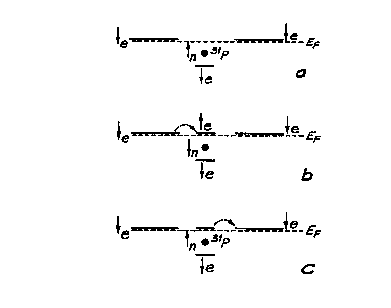
Figure 2 is a schematic diagram of a donor atom weakly coupled to
electron spin polarized reservoirs. In this case the electrons in the
reservoirs
25 and on the donor are polarized in the same direction. In Figure 2a, the
spin
on the donor nucleus is polarized oppositely to the spin on all the electrons
and this permits current to flow by an electron from a reservoir exchanging
spin with the donor nucleus to arrive at the situation shown in Figure 2b. In
Figure 2b, the spin of the donor nucleus has been flipped, and an electron
has passed from the reservoir to the nucleus where it is oppositely polarized
to the existing electron. The electron that has been passed to the nucleus
can pass off to the other reservoir by again exchanging spin with the donor
nucleus. This results in the situation shown in Figure 2c where one electron
has passed from the reservoir on the left to the reservoir on the right and
the
donor nucleus spin has flipped twice to return to its initial condition.
Figure 3 is a schematic diagram of two donors located in a semi-
conductor beneath a metal barrier, on top of which are located metal gates
used to probe the spin system. A-gates are located above the donors, while a
E-gate is located between the donors. By biasing the A-gates above the
donors appropriately, it can become energetically favourable for both
electrons to become bound to the same donor, a state that can only be
singlet. Thus, the detection of charge motion between the two donors can be
detected by changes in the potential on the A-gates, and can be used to infer
the spin of the electrons.
Figure 4 is an energy level diagram of a two electron system in a
magnetic field as a function of the exchange coupling, E. Dashed lines are
CA 02304045 2000-03-15
WO 99/14614 PCT/AU98/00778
8
the energy levels when the spin splitting of the uncoupled electrons are
equal, while solid lines are the energies when one electron has greater spin
splitting energy than the other. The arrows and dotted lines show an
adiabatic sequence of steps that take the ~.~T) state into the spin singlet
state
~ 1'J. -J.1').
Figure 5 is a energy level diagram showing the sixteen energy levels
of the coupled system of two electrons and two nuclei plotted for the case
when the hyperfine coupling constant is equal for each nucleus. The energy
splitting of the nuclei relative to the electrons is greatly exaggerated. At E-
= 0, the four lowest energy levels correspond to ~ ~~~.) electron states. In
the
coupled system, two of the states evolve into triplets and two evolve into
singlets as E-increases.
Figure 6 is an energy level diagram showing the adiabatic evolution
of nucleus spin states prior to measurement, achieved by increasing the
hyperfine coupling of one nucleus spin to the electrons relative to the other.
The state of the left nucleus spin determines whether or not the system will
evolve into the electron singlet state.
Figure 7a is a schematic diagram showing the arrangement of the
source, drain, gate, and island of a single electron tunneling transistor
(SETT). Fig. 7b shows the effect of a Coulomb blockade when there is no
energy level equal to the Fermi level in the source and drain available on the
island. Conduction takes place when there is an energy level in the island
equal to the Fermi level in the source and drain.
Best Modes for Carrying out the Invention
The Pauli Exclusion Principle (that two electrons can occupy the
same quantum state if and only if they have opposite spin) manifests itself in
systems of two or more electrons. Some examples of the invention rely upon
the exclusion principle to measure spin by detecting charge motion into and
out of two electron systems. Because of the Pauli Principle, the energy
levels of two electron systems differ, depending on whether the spins are
aligned (triplet states) or opposed (singlet states).
For clarity, the following discussion is restricted to discussing only
the simplest two electron systems encountered in condensed matter systems:
the system of two electrons bound to a single positive charge (called a D-
CA 02304045 2000-03-15
WO 99/14614 PCT/AU98/00778 -
9
center when the positive charge is a donor in a semiconductor). However, it
should be understood that any two-electron system will have similar
properties.
In general, the only bound state of a D- center is a singlet where the
electron spins are opposed; the triplet states, where the spins are aligned,
lie
in the continuum. In the specific condensed matter system of Si, the D-
center, consisting of two singlet electrons bound to a P donor, has a bound
state energy of -1.7 meV.
Single Electron Spin Valve
Perhaps the simplest conceptual device for single spin measurement
is shown in Figure. 1. A single donor atom 1 is weakly coupled to two
reservoirs of spin-polarized electrons 2 and 3. For example, the electrons
may be polarised by being at low temperature (T~ in a large magnetic field
(B). A single electron 4, whose spin is to be determined, is bound to the
donor. To operate the device, the energy of the donor D' center is made
equal, or.resonant with, the Fermi energy (EF) of the reservoirs. Since charge
transfer across the donor must go through the singlet D- state, current will
only flow, as indicated in Figure 1a, if the spin on the donor is opposite to
the spin polarization in the reservoirs. When the conditions are appropriate
an electron from one of the reservoirs may join the same quantum state (with
opposite spin) as the bound electron, and then depart the donor to the other
reservoir. When the electrons are all polarized in the same direction no
current can flow since the electrons from the reservoir cannot enter the same
quantum state as the bound electron, as indicated in Figure 1b. The
detection of current flow in the device constitutes a measurement of the
single electron spin on the donor.
This assumes that there is no mechanism present to "flip" reservoir
electrons initially pointing in the same direction as the donor electron so
that they can occupy the D- center and traverse between the reservoirs. If
the donor is a nucleus with spin, coupled to the electrons by the hyperfine
interaction, such a process can occur and will enable the nuclear spin to be
measured in appropriate circumstances. The process involves the electron
coming from the reservoir and exchanging its spin with the spin of the
nucleus so that its spin is then opposed to the donor electron and can form a
singlet with it. In Figure 2a, all the electron spins are polarized in the
same
CA 02304045 2000-03-15
WO 99/14614 PCT/AU98/00778 -
direction (again, prepared by an environment with low T and large B.)
Current can now cross the junction if and only if the nuclear spin is
initially
opposed to the electron spins. This "single nucleus spin valve" illustrates
how nuclear spins, coupled to electrons by the hyperfine interaction, can be
5 measured in devices similar to those measuring single electron spins.
Single Spin Measurement using Capacitive Techniques
These single spin valve devices, although illustrative, suffer from
several practical deficiencies. In particular, they require polarized electron
10 spin reservoirs. A small contamination of the reservoirs with electrons of
the wrong spin will lead to device malfunction. Also, the need for reservoirs
may greatly limit their value in certain applications. Both of these
limitations can be circumvented if a closed system is probed, so spin transfer
to and from the system is entirely eliminated. If the system is probed
capacitively, any metallic lead can couple to the system, with no special
requirement for spin-polarized electrons.
Once again, for simplicity and clarity discussion is confined to a
two-electron system. Consider two electrons bound to two positively charged
donors, spaced sufficiently close to each other so that electron transfer, or
exchange coupling, between the donors is possible. These donors are
located in a semiconductor 5 beneath a barrier material 6, on top of which
are located the metal gates used to probe the spin system, as shown in Figure
3. 'A-gates' 7 are located above the donors, while a 'E-gate' 8 is located
between the donors.
Such a system can measure spin if a potential difference is applied to
the two A-gates. As such a voltage is applied, at some point it will become
energetically favorable for both electrons to become bound to the same
donor, that is a D- state. However, as was mentioned above, D- bound states
are only possible if the electrons are in a mutual singlet state. The
signature
of the singlet state, charge motion between donors as a differential bias is
applied to the A-gates, can be detected externally by single electron
tunnelling transistor capacitance electrometry.
Preparation of the Spin States for Measurement
This spin detection method distinguishes between singlet and triplet
states of a two spin system but cannot measure the state of an individual
CA 02304045 2000-03-15
WO 99/14614 PCT/AU98/00778
11
spin. The state of a given spin system can be inferred from the measurement
if the system is appropriately prepared. Here, "preparation" means adiabatic
changes to the spin state energies before the measurement takes place that
ensure that the measurement outcome is determined by the initial state of a
given spin.
The electron spin energies can be slowly varied if the electron g-
factor, that is the coefficient relating the applied DC magnetic field to the
spin energy splitting, is sensitive to the location of the electron or if a
gradient in B is present. Controlling the applied bias to the intermediary E-
gate can also control the exchange coupling of the electrons.
To illustrate the procedure, consider the two spins left or 'L' and
right or 'R' shown in Figure 4, with L pointing down and R the spin to be
determined, or in other words starting with ~ ~~?J.
First, manipulate the A-gates so that spin L has larger energy than
spin R, thus breaking the T.~-~~T degeneracy with L(~.)R(T) having the lower
energy. Next, turn on the exchange coupling between the two electrons. As
the exchange coupling increases, the lower energy state of the two states
with a single spin pointing up evolves into the singlet state, which at large
E-
will have the lowest energy. The A-gates can then be brought back into
balance so that the ground state is an exact singlet. A measurement will
yield the result for a singlet state if and only if the original spin
configuration was L(~.)R(1'). After the measurement the two spins can be
returned to their initial configuration by reversing the sequence of adiabatic
manipulations.
If the state of spin L is unknown, two measurements can be
performed in sequence on the spins, with the second beginning with a spin
flip of spin L. (Since the A-gates control the resanance frequency of the
spins, the L spin can be selectively brought into resonance with an external
AC magnetic field and its state inverted.) The second measurement will
produce a singlet result if and only if the initial state, prior to the first
measurement, was L(T)R(T). A singlet result for one of the two
measurements will occur for R(T) regardless of the initial state of spin L.
Adiabatic Approaches to Nuclear Spin Measurement
If electrons are coupled to donor nuclei by the hyperfine interaction,
the states of the nuclear spins can determine the outcome of the
CA 02304045 2000-03-15
WO 99114614 PCT1AU98/00778 -
12
measurement of the electron spin. This is achieved when the exchange
interaction E enables the ~ T) and the ~ ~.) states of the electron with the
same
energy to overlap, enabling resonant electron- nuclear spin exchange. In the
case discussed above the exchange can occur when the ~.~~~) and the ~ 1'.~ -
~~T) levels cross.
The sixteen separate energy levels for the coupled system of two
electrons and two nuclei are plotted in Figure 5 as a function of the
exchange interaction E-for the case the hyperfine interaction and Zeeman
energy (nuclear and electron spin splitting) of the two sites are equal. (In
the figure, the magnitude of the nuclear level splitting is much exaggerated
compared to the electron level splitting for clarity.) If the two electrons
are
initially in their ground state (L(~~)R(~.)) the two lowest energy nuclear
spin
levels evolve into the singlet state, while the two highest energy nuclear
levels evolve into the triplet state.
If the nuclear spin degeneracy is broken because of A-gate biases, see
figure 6, as was done above for electron spin, then whether or not the system
evolves into a singlet is entirely determined by the initial spin state of the
nuclear spin with the larger splitting. Thus, for the coupled electron-nuclear
spin system, a single measurement can determine the spin state of a chosen
nuclear spin. In Figure 6 the solid lines represent the electron energy levels
as a function of E. The dashed lines represent the lowest energy-coupled
electron-nuclear energy levels as a function of E. The electron energy levels
behave as in Figure 4,
Measuring the Spin State using a Single Electron Tunnelling Transistor
Single electron tunnelling transistors (SETTs)are currently the most
sensitive devices developed to measure small charges and small charge
motions. SETTs contain a small "island" electrode 9 located between source
10 and drain 11 electrodes, as illustrated in Figure. 7a). Current flows from
source 10 to drain 11 only if there is an energy level in the island 9 equal
to
the Fermi level in the source 10 and drain 11, as shown in Figure 7b. The
"Coulomb blockade", as illustrated in Figure 7c, results when no energy level
is available on the island through which the electrons can tunnel. The
extreme sensitivity of SETTs will occur when the island 9 is extremely small
and when the device is at low temperature.
CA 02304045 2000-03-15
WO 99/14614 PCT/AU98/00778
13
For spin detection, designs can readily be implemented, including
the three gate structure shown in Figure 3, where one of the A-gates is also
the island of a SETT. In the scenario where the devices discussed above are
used to measure and initialize spins in a quantum computer, many SETTs
would be necessary to measure many spins simultaneously. The capacitive
coupling technique for spin measurement is particularly attractive, since a
two dimensional array of spins could be measured using electrodes out of
the plane of the spins, and every spin in the array could be independently
measured by a separate SETT device. Thus, this approach to spin
measurement is well suited to future large scale quantum computation.
Such a quantum computer could comprise a Si substrate into which
an array of donor atoms of 3'P are introduced 200 ~ beneath the surface.
The atoms are separated by less than 200 A. ConductingA-gates are laid
down on a Si02 insulating layer above the Si substrate, each A-gate being
directly above a respective 3'P atom. Conducting E-gates are laid down on
the insulating layer between each cell.
The nuclear spins of the donor atoms are the quantum states or
"qubits" in which quantuminformation is stored and manipulated. TheA-
gates control the resonance frequency of the nuclear spin qubits, while E-
gates control the electron-mediated coupling between adjacent nuclear
spins.
In operation, the device is cooled to a temperature of T = 50 mK.
Also, a constant magnetic field of B = 2T is applied to break the two-fold
spin degeneracy. The combined effect is that the electrons only occupy the
nondegenerate lowest spin energy level. The electrons must remain in a
zero entropy ground state throughout a computation.
An electric field applied at theA-gate to the electron-donor system
shifts the electron wave function envelope away from the nucleus and
reduces the hyperfine interaction. A donor nuclear spin-electron system
close to an A-gate functions as a voltage controlled oscillator: the
precession
CA 02304045 2000-03-15
WO 99/14614 PCT/AU98/00778
14
frequency of the nuclear spin can be controlled externally, and spins can be
selectively brought into resonance with an externally applied alternating
magnetic field, BAC=10-3 T, allowing arbitrary rotations to be performed on
the nuclear spin.
Coupling between two donor-electron spin systems will arise from
the electron spin exchange interaction when the donors are sufficiently close
to each other. Significant coupling between nuclei will occur when the
separation between donors is about 100-200 L~.
For two electron systems the exchange interaction lowers the
electron singlet ( ~ T~. - ~.T)) energy with respect to the triplets. In a
magnetic .
field, however, the electron ground state will be polarised if ~cBB > 2~. The
nuclear singlet ~ 10 - 01) (spins 180° out of phase) is lowered in
energy with
respect to ~ 10 + 01) (spins in phase). The other two triplet states are
higher
and lower than these states.
When the voltages of the A-gates is not equal the nuclear spin
singlets and triplets are no longer eigenstates, and the eigenstates of the
central levels will approach ~ 10) and ~ 01) when the voltage difference is
large enough.
Control of the E-gates, combined with control of A-gates and
application of BAC, are sufficient to effect the controlled rotation operation
between two adjacent spins. The action of A-gates and E-gates, together with
BAC Perform all of the reversible operations for quantum computation.
Constructing the Electron Devices
The materials used to build such electron devices must be almost
completely free of spin (I =/ 0 isotopes) and charge impurities in order to
prevent dephasing fluctuations from arising within it. Donors must be
introduced into the material hundreds of t~ beneath the surface. Finally, the
gates with lateral dimensions and separations < 100 ~r must be patterned on
the surface, registered to the donors beneath them. Each of these are the
focus of intense current research in the rapidly moving field of
semiconductor growth and nanofabrication. This research bears directly on
the problems of making a nuclear spin quantum computer in silicon.
An excellent indicator of suitable semiconductor materials is the
ability to observe integral and fractional quantum Hall effects in them. In
particular, the spin detection techniques outlined above require that
CA 02304045 2000-03-15
WO 99/14614 PCT/AU98/00778
electrons can be fully spin polarised, a condition which leads to quantisation
of the Hall effect at integers corresponding to the spin gap. This condition
is
well satisfied in high mobility GaAs/AlXGa1_XAs heterostructures, where
nuclear spin sensing electronics have been demonstrated. Absence of 1=0
5 isotopes, however, in these materials means that making an electron device
from them is highly unlikely. Recent advances in Si/SiXGe1_x
heterostructures have led to materials composed entirely of group IV
elements with quality comparable to GaAs heterostructures. The fractional
quantum Hall effect is observed in these materials and spin splitting is well
10 resolved. Nanostructures have also been fabricated on high quality
Si/SixGel_X heterostructures.
While the quality of SiJSi02 interfaces and the electron systems
confined there is less than that of epitaxial interfaces, spin splittings are
well
resolved at low temperatures. The much larger barrier height in SiOz over
15 Si/SiXGel_X (3.3V vs. -~-0.2 V) is a critical advantage in nanostructures
with
sizes of 100 ~ or less. Leakage of electrons across the barrier material,
resulting in the removal of an electron from a donor state, is a source of
decoherence in the quantum computer not mentioned previously. Electrons
consequently must not tunnel across the barrier during the computation.
Also, the ability of E-gates to vary the exchange interaction over a large
dynamic range will improve in devices with large barrier heights.
Technologies being developed for electronics applications may result in
structures with both the high interface quality of Si/SiXGe1_X and the larger
tunnel barrier of Si02. Because of charge fluctuations and disorder, it is
likely that bulk and interface states in SiOZ will need to be reduced or
eliminated if an electron device is to be fabricated using SiOz.
The most obvious obstacle to building the electron devices presented
above is the incorporation of the donor array into the Si layer beneath the
barrier layer. Currently semiconductor heterostructures are deposited layer
by layer. The b-doping technique produces donors lying on a plane in the
material, with the donors randomly distributed within the plane. The
electron devices envisioned require that the donors be placed into an
ordered array making it extremely difficult to create the array by using
lithography and ion implantation or by focused deposition. Methods
currently under development to place single atoms an surfaces using ultra
high vacuum scanning tunnelling microscopy are likely candidates to be
CA 02304045 2000-03-15
WO 99/14614 PCT/AU98/00778
16
used to position the donor array. This approach has been used to place Ga
atoms on a Si surface. A challenge will be to grow high quality Si layers on
the surface subsequent to placement of the donors.
Because the donors in the array must be <200 ~ apart in order for
exchange coupling between the electron spins to be significant, the gate
dimensions must be < 100 ~, although the separations may be larger if the
E-gates are biased positively to reduce the barrier between donors. In
addition, the gates must be accurately registered to the donors beneath them.
Scanned probe lithography techniques have the potential to sense the
location of the donors beneath the surface prior to exposing the gate patterns
on the surface. For example, a scanning near field optical microscope could
be used to detect the photoluminescence characteristic of the P donors in a
wavelength range that does not expose photoresist. After P detection and
proper positioning of the probe, the resist is exposed with a different light
wavelength. "Custom patterning" of the gates may prove to be necessary to
compensate for irregularities or defects in the placement of the donor array.
Many of the technical challenges facing the development of such
electron devices are similar to those facing the next generation of
conventional electronics; consequently, tremendous efforts are already
underway to overcome these obstacles.
It will be appreciated by persons skilled in the art that numerous
variations and/or modifications may be made to the invention as shown is
the specific embodiments without departing from the spirit or scope of the
invention as broadly described. The present embodiments are, therefore, to
be considered in all respects as illustrative and not restrictive.