Note: Descriptions are shown in the official language in which they were submitted.
CA 02304525 2000-03-24
WO 99/17425 PCT/SE98/01715
1
Insulation for a conductor
TECHNICAL FIELD
The present invention relates to an insulation for, and a
method for insulation of, a conductor arranged in a
plurality of turns for generation of a magnetic field. In
particular, the invention relates to an insulation in an
electric circuit in a rotating electrical machine. By a
rotating electrical machine is meant an apparatus which
converts electrical energy into mechanical energy or vice
versa. Such an apparatus comprises an electric circuit, a
magnetic circuit, and a mechanical circuit. The mechanical
circuit comprises two bodies which are movable in relation
to each other. Upon a forced mechanical movement, a
magnetic field is generated which is converted by the
electric circuit into electrical energy. V~Then supplying
electrical energy, a magnetic field is generated which is
converted by the mechanical circuit into mechanical
energy. By a rotating electrical machine, as used in the
following text, are meant both a generator and a motor.
The invention is preferably intended to be applied to a
rotating electrical machine acting under high current and
under high voltage, such as, for example, a generator
which produces electric power. The mechanical circuit here
comprises a stator and a rotor, whereby the rotor is
rotatable in relation to the stator with one degree of
freedom. The electric circuit may be arranged as a winding
in either the rotor or the stator, or in both. By
electrifying a winding, a magnetic field arises between
the rotor and the stator. The magnetic field may be
controlled and amplified by arranging magnetic cores in
the stator and the rotor, which magnetic cores may be
composed of, for example, laminated stacks of magnetically
oriented sheets. However, the invention is not limited to
an application on rotating electrical machines only, but
may also be used in any electrical machines or apparatus
CA 02304525 2000-03-24
WO 99/17425 PCT/SE98/01715
2
in which a conductor is to be insulated to be able to
handle high voltages.
BACKGROUND ART, THE PROBLEM
To be able to describe the meritorious properties of the
invention, a rotating machine in the form of a generator
will be briefly described here. The most frequently used
type of generator in force applications is a so-called
synchronous machine. Such a machine comprises a rotatably
journalled rotor with a rotor winding surrounded by a
stationary stator with a stator winding. Both the rotor
and the stator comprise magnetizable material, which
preferably consists of laminated stacks of sheet. By
supplying mechanical energy to the rotor shaft, the rotor
is brought into a constant rotating movement. A current is
caused to flow in the rotor winding, whereby a rotating
magnetic field arises which generates a current in the
stator winding.
The stator winding is arranged in radially embedded slots
in the stator. The slots are axially oriented and
rotationally symmetrically distributed along the stator.
The stator winding comprises one or more series-connected
conductors which are arranged in coils, which are located
in the slots with two coils per slot. In ac machines a
variation of the inductance across the cross section of
the winding conductor arises. The greatest reactance is
obtained at the bottom of the conductor and the main part
of the current then tends to flow at the top of the
conductor. To counteract such a current displacement, the
conductor is divided into a plurality of strands which are
insulated from one another. The division into strands does
not prevent the inductance from varying for the different
strands, but these have to be transposed, that is, change
places. Such a transposition is usually carried out
outside the stack of sheets but may also be arranged in
the slots by means of a so-called Roebel transposition.
CA 02304525 2000-03-24
WO 99/17425 PCT/SE98/01715
3
The choice of strand dimensions is a compromise between
electrical and mechanical requirements. From an electrical
point of view, it is preferable to have many strands since
this reduces the current displacement, but from a
mechanical point of view, the coils may become more
difficult to manufacture and install. Few strands with
large dimensions result in problems when, for example, a
conductor is to be bent.
When insulating high-voltage windings, inter alia thermal,
electrical, environmental and mechanical stresses must be
taken in to consideration. These are usually called TEAM
(Thermal, Electrical, Ambient and Mechanical) and
influence the life of the insulation to a greater or
smaller extent. From a thermal point of view, the
insulation shall allow a temperature increase which may
comprise 0-180°C within one hour. From an electrical point
of view, the insulation shall permit a satisfactory
electrical insulation without causing concentrations of
the electric field. From the ambient, or environmental,
point of view, the insulation shall not be influenced by
dirt, ozone or condensation. Nor shall the insulation,
from the environmental point of view, entail any
environmentally harmful emissions during manufacture or
operation, and, during scrapping, be capable of being
recycled. Finally, from a mechanical point of view, the
insulation shall allow the coils to be fixed to the stator
but still allow movement during thermal expansion of the
conductor and insulating material.
Although the voltage between the conductors is higher than
between the strands, the conductor and strand voltages are
relatively low. The strand and conductor insulation is
therefore often simple to carry out. However, the coil
itself must withstand the entire phase voltage which may
amount to several kV. To this end, the coil is insulated
against the stator by a main insulation. At high potential
differences, a partial discharge, or PD, easily arises,
CA 02304525 2000-03-24
WO 99/17425
PCT/SE98/01715
4
because of deformations of the field in the high electric
field strength, this partial discharge being commonly
referred to as corona. When corona occurs, ozone (0,)
arises, among other things, which is very aggressive
towards organic compounds. Thus, corona causes a weakening
of organic insulating materials and the main insulation
therefore includes materials which are corona-resistant.
One such material is mica, which is an inorganic compound
and which withstands the attack of ozone.
The most commonly used insulating materials contain mica
as main component. The mica is often embedded into a
binder which is arranged on a tape-formed carrier. The
material of the carrier and the binder may vary. A common
embodiment of the main insulation is in the form of resin-
saturated tapes containing flakes of mica, which are wound
around the conductor and then cured in a furnace proce-
dure. On top of the main insulation, a corona protector is
arranged, which is to prevent external corona between the
coil side and the slot wall.
Mica is a very brittle material which has low shear
strength. Mica also has a thermal expansion which is one-
fifth of, for example, that of copper. When loading an
electrical machine, the winding is subjected to a
temperature rise. The conductor, which is often made of
copper, then tends to expand more than the insulation.
Between the conductor and the insulation, a voltage thus
arises because of the different thermal properties of the
materials. Since mica has lower shear strength, fractures
thus arise, which give rise to cavities in the insulation.
Eventually, the cavities are filled with air and give rise
to considerable deformations of the electric field. At
such field concentrations, corona arises.
From US 5,066,881, an insulation for a generator is
previously known, the main task of which is to arrange, in
contact with the outside of the main insulation, a layer
CA 02304525 2000-03-24
WO 99/17425
PCT/SE98/01715
which is capable of diverting charges to minimize corona.
To this end, the insulation is surrounded by a semicon-
ducting layer of a curable glass-fibre coating. This
coating replaces a prior art grounding tape, which had the
5 ability to divert charges for preventing corona. The new
coating is stated to conform to the contour of the
insulation in a better way and to better retain its
semiconducting properties after the curing of the main
insulation. In one embodiment, the semiconducting layer is
applied to the upper and lower end regions of a coil on
the inside of the main insulation. This embodiment is
stated to entail an equalized electric equipotential
around the ends. The known insulation does not add
anything new to the prior art technique. Thus, it was
already previously known to divert charges by arranging a
semiconducting layer outside the insulation.
The predominant problem during insulation of a rotating
electrical machine, such as a generator or a motor, is
that the insulant and the conductor have different thermal
expansion. In case of temperature variations, this implies
that the insulant and the conductor are displaced in
relation to each other such that cavities arise. The
electric field is greatest nearest the conductor. Cavities
thus arise where the risk of corona is greatest. In known
generators, a certain amount of corona is accepted and
instead the insulation is brought to contain mica which
withstands discharges. As discussed above, mica has
inferior mechanical properties. when the discharges occur,
ozone is formed which attacks carriers and binders of the
insulation, gradually resulting in the insulation burst-
ing. Thus, after a certain time, the stator winding with
the insulation must be replaced.
An additional problem in the known electrical machines
where corona is accepted is that the discharges cause
electromagnetic disturbances, which results in sensitive
CA 02304525 2000-03-24
WO 99/17425 PCT/SE98/01715
6
electronic equipment being disturbed or, even, ceasing to
function.
SUMMARY OF THE INVENTION
The object of the invention is to produce an insulation
for a conductor arranged in a plurality of turns for
generating a magnetic field. In particular, the invention
relates to an insulation, arranged at a rotating elec-
trical machine, which eliminates the occurrence of partial
discharges (PD) and which has a long service life. The
insulation shall also entail reduced maintenance and be
more reliable than previously known insulation systems.
From an environmental point of view, the insulation shall
entail less environmentally harmful emissions during
manufacture, use as well as scrapping. The object of the
invention is also to suggest a method for insulation of a
rotating electrical machine while achieving the objectives
stated above. The insulation is in particular suitable
when replacing a winding for an existing electrical
machine.
The above object is achieved according to the invention by
an insulation according to the characteristic features
stated in the characterizing part of the independent
claims 1 and 8 and with a method according to the
characteristic features stated in the characterizing part
of the independent method claim 9. Advantageous embodi-
ments are stated in the characterizing parts of the
dependent claims.
An electrical insulation is a medium or a material which,
when placed between conductors of different potential,
allows only a small or insignificant current to pass
therethrough. At an increased potential between the
conductors, also the electric field strength across the
insulation increases. This also increases the risk of
breakdown since the dielectric strength of the material is
CA 02304525 2000-03-24
WO 99/17425 PC'T/SE98/01715
7
exceeded. The electric strength is defined as the maximum
voltage gradient which the material is able to withstand
without breakdown occurring.
The dielectric breakdown for a gas is a result of an
exponential multiplication of free electrons induced by
the applied electric field. In a constant electric field,
breakdown occurs at a voltage which is a function of the
product of pressure and distance. Here, both in case of a
small and a large such product, a gas has a high breakdown
strength. In case of a small volume and a high pressure,
an electron accelerated by the electric field is not able
to pick up sufficient acceleration for starting a break-
down by collision with other electrons. In case of a
larger volume and a low pressure, the number of electrons
is too small in order for a sufficient number of colli-
sions to take place. Under the proper conditions, an
electron is accelerated to such a speed that, upon colli-
sion with other electrons, these are accelerated in a
similar manner whereby an avalance-like breakdown occurs.
In a practical application, the dimensioning dielectric
strength for a gas is about 0.5 kV/mm. At lower electric
field strengths, thus, no corona occurs in gas-filled
cavities in the insulating material or between conductors
and insulation.
Within high-field engineering, that is to say, when the
electric field strength exceeds the dielectric strength
for a gas, the risk of corona is obvious. A cavity which
contains a gas in the insulant here entails spontaneous
discharges. Thus, there is a considerable need to be able
to minimize or completely exclude cavities in the insula-
tion between conductor and insulation and to arrange the
electric field such that field concentrations are avoided.
The insulation according to the invention comprises an
elongated tubular insulant intended to enclose a conduc-
tor. The insulant has one inner and one outer semicon-
CA 02304525 2000-03-24
WO 99/17425
PCT/SE98/01715
8
ducting layer adapted to contain between themselves an
electric field. The semiconducting layers cover the inside
and the outside, respectively, of the insulant and are
joined to the insulant with such an adhesion that the
materials accompany each other in case of a structural
change caused, for example, by thermal or mechanical
stresses. Thus, the joint must not contain cavities,
neither during manufacture nor in cases of stresses on the
joined-together materials. Such an adhesion between the
insulant and the two semiconducting layers is achieved by
manufacturing them from the same materials. In case of a
change in temperature, the materials then expand equally,
whereby no, or only small, forces arise across the joint.
However, adhesion may also be obtained between materials
with different mechanical or thermal properties. For
example, a joint with the adhesion aimed at may be
achieved by heat treatment of the materials such that they
float together at the joint into a homogeneous structure.
Mechanical or thermal changes between the insulant and the
two semiconducting layers are then absorbed as elastic or
plastic deformations in the materials nearest the joint.
The inner layer is adapted to be galvanically or capa-
citively coupled to the conductor and the outer layer is
adapted to be connected, for example, to ground or another
controllable potential, whereby the electric field arisen
between the conductor and ground is enclosed between the
semiconducting layers in the insulation. Any cavities
which may arise inside the insulation, because of a change
in temperature or mechanical influence, do not give rise
to any occurrence of PD. Between the conductor and the
inner semiconducting layer, there is no potential
difference.
By ensuring that corona does not occur, in the manner
described above, the insulant may be made of an organic
material without any addition of mica. The full insulating
capacity of the material may then be utilized. Since no
CA 02304525 2000-03-24
WO 99/17425 PCT/SE98/01715
9
ozone is formed which may weaken the materials, the
thickness of the insulation may be made smaller. The
insulation may therefore be made of a homogeneous
material, for example a thermoplastic resin or a rubber
mixture. One such suitable material is a crosslinkable
polyethylene. The semiconducting materials may be made of
the same material and be brought to contain a conducting
dust, for example carbon black or powdered coal. The
insulant with the two semiconducting layers may hence in a
simple manner be applied to the conductor by, for example,
extrusion.
The insulation system is especially intended for coils
with a plurality of conductors, which may be divided into
strands. The conductor and strand insulation is suitably
made of a material which has a higher permittivity than
the main insulation. By this arrangement, the insulation
lying inside the inner semiconducting layer of the main
insulation is able to change the electric field such that
the concentration across the inner insulation becomes
smaller. Instead the inner insulation "presses" out the
equipotential lines in the field such that the larger
concentration occurs within the main insulation. By this
change of the field, the larger concentration is also
brought to propagate over a larger area, the field
concentration thus being thinned out.
In case of a lightning stroke, for example, an electrical
rotating machine is subjected to an electric shock. During
one or a few microseconds, the voltage then rises in the
winding. Between conductors in a coil the potential
difference may then amount to a few tens of kilovolts.
Each conductor strand is surrounded by a thin strand
insulation which is adapted to insulate the conductor
strands from each other. The strand insulation is usually
adapted to exhibit a good short-term strength against
electric flashovers. Two conductor strands are thus
insulated from each other with an insulation thickness
CA 02304525 2000-03-24
WO 99/17425 PCT/SE98/01715
corresponding to two strand insulations. Likewise, between
conductor strands associated with different conductors in
a coil, two layer thicknesses of this insulation are
arranged. Thus, flashovers in case of a shock between
5 these occur only infrequently.
Since an insulation according to the invention encloses a
plurality of conductors, the insulation between the semi-
conducting layer and a conductor strand making contact
10 therewith constitutes the thickness of the actual strand
insulation only. The semiconducting Layer is suitably
connected to one of the conductor strands belonging to one
of the conductors. The potential difference between the
semiconducting layer and the conductor strand positioned
nearest thereto is then only a few hundred volts during
normal operation. The strand insulation constitutes
sufficient insulation for preventing a flashover. In case
of a shock, the potential increases instantaneously to
several kilovolts. However, this potential change does not
have time to develop into full strength in the semicon-
ducting layer, so probabaly no flashover occurs in this
case either.
The insulation referred to here permits a corona-free
environment during normal operation. This implies that
organic insulating materials may be utilized also for the
strand insulation. This opens up new possibilities for
considerably more elegant solutions of insulation than in
an environment where corona occurs. Organic insulants with
improved properties may be chosen and the insulating
layers may be made thinner. To safely manage the insula-
tion between the conductor strands and the inner semi-
conducting layer, each conductor, including all the con-
ductor strands, may be coated with an extra layer of high-
quality insulating material.
CA 02304525 2000-03-24
WO 99/17425 PCT/SE98/01715
11
BRIEF DESCRIPTION OF THE DRAWING
The invention will be explained in greater detail by
description of an embodiment with reference to the
accompanying drawing, wherein
Figure 1 shows a cross section through a coil for a stator
winding which comprises an insulation according
to the invention, and
Figure 2 shows a cross section of an insulation according
to the invention with a circular cross section,
said insulation enclosing two conductors.
DESCRIPTION OF THE PREFERRED EMBODIMENT
A cross section through a typical winding coil for a
rotating electrical machine is shown in Figure 1. The
winding comprises a first conductor with a plurality of
strands 2 and a second conductor also with a plurality of
strands 3. The strands belonging to the respective
conductor are surrounded by a strand insulation 4, which
thus forms an insulating layer surrounding the stack of
conductor strands. Surrounding the strand insulation 4 is
an insulation 1, which comprises an insulating
intermediate layer 6 with an inner semiconducting layer 5
and an outer semiconducting layer 7.
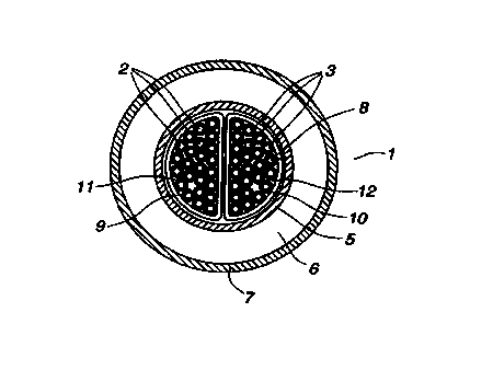
Figure 2 shows a cross section of an insulation 1 which
encloses a first conductor 11 comprising a plurality of
conductor strands 2 and a second conductor 12 comprising a
plurality of conductor strands 3. The first conductor is
surrounded by an insulating layer 9 and the second con-
ductor is surrounded by an insulating layer 10. The
surrounding insulation 1 comprises an insulating inter-
mediate layer 6, an inner semiconducting layer 5 and an
outer semiconducting layer 7. In the figures, the
different layers have been intentionally made thick so as
CA 02304525 2000-03-24
WO 99/17425
PCT/SE98/01715
12
to emphasize them. In reality, the semiconducting layers
are thin and the insulating layers enclosing the conductor
and the conductor strands are very thin. When manufac-
turing an insulation according to the invention, and
conductors and conductor strands enclosed therein, the
insulating layers tend to be compressed into a homogeneous
insulation surrounding conductors and conductor strands.
One conductor strand 8 is galvanically or capacitively
coupled to the inner semiconducting layer 5, such that
this layer assumes the same potential as the conductor
strand 8. The outer semiconducting layer 7 is in elec-
trical connection with ground. By this arrangement, the
insulation 1 is brought to contain the electric field
which is formed between the conductor and ground. Of
particular importance for the function of the insulation
is that no cavities are formed between the inner semi-
conducting layer and the outer semiconducting layer. The
insulating layer and the two semiconducting layers must be
homogeneous and be in absolute mechanical contact with one
another. The mechanical contact must also be maintained in
case of a change caused by temperature variation or
mechanical influence.
The outer semiconducting layer is adapted to distribute
the ground potential across the outer limiting surface of
the insulation. The outer semiconducting layer must thus
cover the entire envelope surface. Similarly, the inner
semiconducting layer is adapted to distribute the phase
voltage connected to the conductor across the inner
limitation of the insulation. The inner semiconducting
layer must thus cover the entire inner limiting surface of
the insulation. In this text, the term semiconducting
material means a material which has considerably less
conducting properties than a conductor but which still
does not have such poor conducting properties that it may
be regarded as an insulant. For example, the material
CA 02304525 2000-03-24
WO 99/17425
PCT/SE98/01715
13
included in the two layers may have a resistivity in the
interval 10-° S2m - 10° S2m, and especially in the interval
1 S2cm - 10 0 SZm .
The insulating intermediate layer is arranged from an
insulating material which has a high electric strength,
for example in excess of 7 kV/mm. By bringing both
semiconducting layers to contain the whole potential
difference between ground and phase and since no cavities
are present between these, no partial discharges arise.
The insulating intermediate layers may thus be arranged
from an organic material, for example a thermoplastic
resin or a rubber mixture. The two semiconducting layers
may advantageously be made of the same material as the
insulating intermediate layer, in which case a conducting
dust, such as carbon black or powdered coal, is mixed into
it. A suitable material is, for example, a cross-linkable
polymer.
A considerable advantage in relation to prior art is
obtained in that the insulating material no longer has to
be supplied by winding. The polymeric material is
advantageously supplied by extrusion, in which case the
two semiconducting layers are supplied in the same
process. This guarantees that cavities are completely
excluded. It is not necessary for the insulant and the
semiconducting layers to be made of the same materials.
The decisive point is that no cavities arise between the
materials. To this end, two separate materials may be
joined together in such a way that the adhesion between
them is maintained during thermal or mechanical influence.
In case of materials with different properties, stresses
arise in the region around the joint since one of the
materials tends to expand more than the other. The
adhesion should therefore be so strong that the joint is
able to absorb these stresses. This can be done by elastic
or plastic deformation of the materials on either side of
the joint. An important advantage of the polymeric
CA 02304525 2000-03-24
WO 99/17425
PCT/SE98/01715
14
material is that it is deformable and may be subjected,
during its service life, to repeated mechanical deforma-
tion without jeopardizing the adhesion between the layers.
Such materials may be simply fused together while
supplying heat, such that the materials float together and
form a homogeneous joint without cavities.
The strand insulation 4 is advantageously arranged with a
dielectric constant which is higher than the dielectric
constant for the main insulation. By this condition of the
material, the strand insulation causes a change of the
electric field such that the equipotential lines are dis-
placed in a radial direction. The concentration of the
electric field, which would otherwise be greatest nearest
the conductor, is thereby displaced out from the centre
and occurs in the main insulation between the two semi-
conducting layers. A larger distance from the centre also
implies that the electric field is distributed over a
larger area, which further weakens the concentration.
To withstand the load caused by an electric shock, for
example from a lightning stroke, an insulating layer is
arranged around each conductor. The potential difference
between conductor strands associated with different
conductors may, in the event of a shock, amount to a few
tens of kilovolts. The short-time strength against
flashovers of a simple layer of strand insulation is
usually not sufficient for stopping a flashover between
the conductor strand and the semiconducting layer. To
safely maintain a sufficient resistance to such flash-
overs, the conductors are enclosed by an extra insulating
layer 9, 10. It is also possible to create sufficient
safety against flashovers by providing the inner semi-
conducting layer with such a resistance that no harmful
potential is able to propagate in case of a shock.