Note: Descriptions are shown in the official language in which they were submitted.
CA 02304782 2000-03-21
WO 99/15883 PCT/US98/19832
1
NONDESTRUCTIVE TESTING OF DIELECTRIC MATERIALS
The benefit of the September 25, 1997 filing date of United States application
serial
number 08/935,074 (now converted to provisional status) is claimed under 35
U.S.C. ~ 119(e)
in the United States, and is claimed under applicable treaties and conventions
outside the
United States.
TECHI~TICAL FIELD
This invention pertains to an apparatus and method for the nondestructive
testing of
dielectric materials, particularly to nondestructive testing with microwaves.
BACKGROUND ART
There is an unfilled need for improved, nondestructive means to test
dielectric
materials for flaws, defects, and irregularities.
An example of this unfilled need is that for improved, nondestructive means
for
inspecting rubber expansion joints. Although this invention has numerous
applications and is
by no means limited to the inspection of rubber expansion joints, that
particular use will be
described briefly because it played a significant role in inspiring the
conception of this
invention.
Most steam-cycle electric power plants employ rubber expansion joints between
the
condenser and the turbine. The expansion joints have multiple composite
layers. Typical
dimensions for such an expansion joint are in the neighborhood of 40 meters
circumference,
by 25 cm wide, by 1 cm thick. Under normal operating conditions, there is a
vacuum on the
inside of the joint, and 1 atm pressure on the outside. Thus when such a joint
fails, it is
prone to catastrophic failure.
A defect can begin, for example, when a small crack allows moisture inside the
rubber. Moisture can then wick along the cords that form part of the
composite. The
moisture can cause the cord to deteriorate, which can lead to adjacent layers
delaminating
CA 02304782 2000-03-21
WO 99/15883 PC"T/US98/19832
2
from one another. Defects such as these inside a joint are difficult to detect
nondestructively
through conventional means.
It is highly desirable that a testing procedure be nondestructive, and be
usable whether
the plant is running or idle. Furthermore, because the access space outside
the joint can be as
little as 7-10 cm, any portion of the detection machinery that must be in
contact with the joint
(or in the vicinity of the joint) should be small enough to fit into such a
space.
If the joint were made of metal, then well-established ultrasonic inspection
techniques
could be used. However, ultrasonic inspection cannot be used for rubber or
soft plastic,
because the polymers absorb nearly all sound energy, and reflect essentially
none. The mesh
or fabric of a composite material so highly scatters and disperses the
ultrasonic waves that an
extremely noisy reflection results. Eddy current measurements or magnetic
measurements do
not work welt in rubber either, because rubber does not conduct electricity.
Neither is radiography particularly helpful. X-ray radiation is used to detect
changes
in bulk density. Under most operating conditions the most common flaw leading
to failure is
delamination. In a delamination failure, an essentially two-dimensional
separation occurs
between adjacent component layers. This separation between layers does not
typically result
in a detectable change in local density, and is therefore not detectable in a
radiograph.
The current state of the art for nondestructive testing of rubber parts is to
use a
Durometer, a needle that penetrates a portion of the rubber, and connects to a
strain gauge.
Durometers have poor practical utility, but they represent the best technology
currently
available for non-destructive testing of rubber joints.
An overview of microwave testing techniques may be found in A. Bahr, Microwave
Nondestructive Testing Methods (1982).
Several microwave nondestructive testing techniques are disclosed in A. Lucian
et al.,
"The Development of Microwave NDT Technology for the Inspection of Nonmetallic
Materials and Composites," pp. 199-232 in Proceedings of the Sixth Symposium
on
Nondestructive Evaluation of Aerospace and Weapons Systems Components and
Materials (San
Antonio, TX 1967).
J. Kurian et al., "Microwave Non-Destructive FIaw/Defect Detection System for
Non-
Metallic Media Supported by Microprocessor-Based Instrumentation," J.
Microwave Power
and Electromagnetic Energy, vol. 24, pp. 74-78 (1989) discloses a method for
detecting
defects in a tire by measuring transmission of microwaves from a dipole
transmitting antenna
inside the tire, through the treads of the tire, with transmission detected by
a linear array of
CA 02304782 2000-03-21
WO 99/15883 PCTNS98/19832
3
detectors. Differential rates of transmission were correlated with changes in
thickness or with
defects.
C. Howell et al., The Use of Low Cost Industrial AM CW 'Microwave Distance
Sensors' for Industrial Control Applications (no date) discloses a microwave
distance sensor to
measure distances to an object from about IS centimeters to about 6 meters
away, by
measuring the phase angle of a returned amplitude-modulated microwave signal
reflected from
the object.
United States patent no. 3,278,841 discloses a microwave flaw detection
system,
particularly for use with large, solid-propellant rocket motors. Microwaves
were transmitted
from inside the propellant, reflected off a metal casing, and detected by a
receiver displaced
from the microwave transmitter. Irregularities in the strength of the received
signal were
correlated with cracks or other flaws in the propellant.
United States patent no. 4,520,308 discloses a system for measuring the
thickness of a
dielectric material by measuring the phase shift of microwaves transmitted
along a microwave
strip line conductor that is adjacent to the material whose thickness is being
measured. See
also United States patent no. 4,123,703.
United States patent no. 2,999,982 discloses a Doppler-effect-based method for
microwave detection of homogeneity defects in compact materials such as
polished glass.
Relatively high speeds of scanning were used to generate the desired Doppler
effect. In the
one example given, the relative speed of the glass versus the detector was 650
centimeters per
second.
United States patent no. 3,144,601 discloses a method for microwave detection
of
non-homogeneous zones in non-conducting materials such as glass sheets and
plates.
Detection was performed by simple measurement of the echoes of the reflected
microwaves;
by measuring losses in intensity following transmission through the object; or
by mixing
incident and reflected waves to create beats, particularly when the material
being examined
was traveling (i.e., detecting Doppler shifts in the frequency of the
reflected microwaves).
United States patent no. 3,271,668 discloses the use of microwaves to measure
the
rate of progressive attrition from a surface of a body of a solid dielectric
material; for
example, measuring the burning profile in a solid rocket motor. Microwaves
were transmitted
through the fuel (or other material), the surface of which reflected some of
the microwaves
back to a detector. The relative phase of incident and reflected microwaves
varied as the
distance from the microwave transmitter to the surface of the burning fuel
changed, allowing
the distance to the surface of the fuel to be determined as a function of
time.
CA 02304782 2000-03-21
WO 99/15883 PCT/US98/19832
4
United States patent no. 4,707,652 discloses a technique for detecting
impurities in a
bulk material by measuring changes in the scattering of microwave radiation
incident on the
bulk materiai.
United States patent no. 4,514,680 discloses a method for detecting knots in
lumber,
by transmitting microwaves through the lumber from two sources of the same
intensity, but
with a 180° phase shift. Transmitted microwaves are detected on the
opposite side of the
lumber. If the lumber is knot-free, there is a null in the microwave field at
the detectors, but
if a knot is present the phase and amplitude of microwave radiation at the
detectors are
altered.
United States patent no. 4,581,574 discloses a method for determining the
average
dielectric constant of a dielectric material having a conductive surface, by
transmitting
microwaves from two transducers into a sheet of the material, and making
measurements of
the energies of reflected microwaves. By measuring average dielectric
constants along a
plurality of paths in the plane of the sheet, locations of variations within
the sheet may be
identified.
United States patent no. 4,274,288 discloses an acoustic, interferometric
method for
measuring the depth of a surface flaw such as a crack.
United States patent no. 4,087,746 discloses a method for determining optical
anisotropy in a dielectric material by measuring changes in the polarization
of microwaves
transmitted through the material.
DISCLOSURE OF INVENTION
A novel apparatus and method have been discovered for the nondestructive
inspection
of dielectric materials. Monochromatic, phase coherent electromagnetic
radiation, preferably
in the 5 - 50 gigahertz frequency range (i.e., microwave radiation) impinges
on the sample.
In accordance with Snell's law, the microwaves are partly transmitted and
partly reflected at
each interface where the dielectric constant changes (e.g., where there are
delaminations,
cracks, holes, impurities, or other defects.)
A portion of the transmitted beam is combined with the signal reflected by the
specimen being inspected. These two signals have the same frequency, but may
differ in
amplitude and phase. The signals combine to produce an interference pattern, a
pattern that
changes as the specimen changes, or as the position of the specimen changes
relative to that of
the detector. Appropriate processing of the interference signal can greatly
improve the signal
to-noise ratio. The detector may be scanned relative to the specimen at any
desired speed,
and the scanning speed need not be uniform. The novel detection technique is
not based on
CA 02304782 2000-03-21
WO 99/15883 PCTNS98/19832
Doppler-shifts in frequency, which result from motion, but rather is based on
interference
between reflected and reference microwaves having substantially the same
frequency, where
the interference is caused by changes in location (independent of motion per
se).
The novel technique can detect cracks, voids, foreign material inclusions
(e.g., water
or oil), thickness changes, delaminations, changes in dielectric constant
(which in rubber may,
for example, indicate aging), and other defects in essentially any dielectric
materials.
Different types of defects have distinguishable characteristics. The technique
can also be
successfully used on composite materials containing conductive components, but
whose
construction makes them overall nonconductors -- for example, carbon fiber
composites.
Substances such as fiberglass that produce noisy reflection patterns in prior
ultrasonic
techniques may be inspected at low noise levels with the novel microwave
technique. The
novel technique readily detects many common defects in fiberglass.
BRIEF DESCRIPTION OF THE DRAWINGS
Fig. 1 depicts a schematic diagram of one embodiment of a defect measurement
device
in accordance with the present invention.
Fig. 2 illustrates how the number of spherical wavefronts from interrogating
radiation
crossed during scanning varies as a function of depth.
Fig. 3 illustrates a calibration of the number of wavefronts crossed by
defects during
scanning as a function of depth.
Figs. 4(a) and 4(b) depict scans of a deeper defect, and a shallower defect,
respectively.
Fig. 5 depicts a scan of a test specimen of polymethylmethacrylate with a hole
drilled
into the bottom surface.
Fig. 6 depicts a slower scan of the same specimen tested in Fig. 5.
Fig. 7 depicts a scan of a particle board into which three wood screws had
been
placed.
Figs. 8 and 9 depict a displacement domain scan over one of the screws in the
particle
board of Fig. 7, with the scan taken from different distances from the screw.
Fig. 10 depicts a preliminary calibration curve of depth versus spatial
frequency of the
interference pattern.
Fig. 11 depicts a scan of an artificial defect in an expansion joint.
CA 02304782 2000-03-21
WO 99/15883 PCT/US98/19832
6
MODES FOR CARRYIrIG OUT THE INVENTION
The novel method and apparatus have been successfully tested in a prototype
embodiment. The microwave transmitter/detector was small, and readily suited
for use in
environments in which access space may be limited.
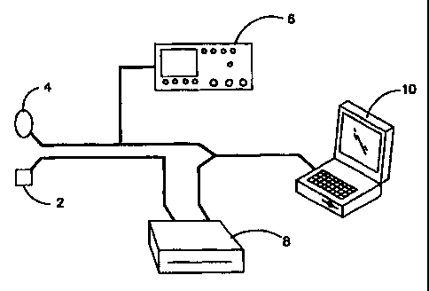
A schematic diagram of one embodiment of the apparatus is illustrated in Fig.
1.
Transducer 2 and optical encoder 4 received regulated DC power from power
supply 6.
Signals from transducer 2 and (optionally) optical encoder 4 were transmitted
to amplifier 8,
which amplified and conditioned the signals before sending them to computer
10. In addition
to the elements ordinarily found in a modern personal computer, computer 10
also included a
16-bit, analog-to-digital data acquisition system, and an input board for
input wiring
terminations. The computer was programmed with software whose function is
described
below.
The Transducer
A preferred transducer 2 was the Gunnplexern transducer (M/A-COM Semiconductor
Products, Burlington, MA), a small and efficient microwave generator based on
a gallium
arsenide junction diode. See, e.g., B. Hale (ed.), The 1989 ARRL Handbook for
the Radio
Amateur, pp. 32-57 & 32-58 (66th ed., i988); The Microwave Gunnplexer~": An
Introduction
(various authors, no date); M/A-COM Semiconductor Products, Varactor Tuned
Gunnplexer~"
Transceiver "Front End" (1985); Microwave Associates, Varactor Tuned Gunn
Oscillator
Transceivers for Commercial Applications (1977). The transducers that were
used in
prototype embodiments of the invention were tunable 10 or 25 gigahertz
Gunnplexer~"
transceivers (frequencies could be higher or lower if desired, e.g., 5 - 50
GHz). The
transceiver could be used with or without a horn waveguide. The detector was a
microwave
frequency diode incorporated as part of the Gunnplexer"' assembly. The
detector diode was
located inside the out-going radiation beam, between the aperture and the
front surface of the
transducer housing. The Gunnplexer"' transducer is frequency stable, and
requires only a 5-
10 Volt DC power supply to produce the desired microwave output energies. It
was mounted
in a hand-held housing, and was connected to signal processing electronics and
data
acquisition hardware via a multiple conductor coaxial cable.
The hand-held unit also contained an optical encoder mounted to a wheel for
measuring the position or displacement of the transducer. The optical encoder
output fed to
one input channel of the PCMCIA-based data acquisition system, which was
located in the
inspection system portable ("notebook") computer.
CA 02304782 2000-03-21
WO 99/15883 PC'T/US98/19832
7
Signal Processing and Power Supply
The detection diode was located at a fixed position within the path of the
outgoing
microwave beam, so that the output signal had a constant amplitude and
frequency.
Microwaves radiated from the transducer to the specimen being tested. Each
time the beam
came to an interface between materials of different dielectric constants
(e.g., the interface
between the air and the specimen, or the interface between the bulk specimen
and a flaw
within), a portion of the energy in the beam was transmitted, and a portion
reflected. The
portion reflected depended on the angle of incidence, the differential in the
dielectric constants
between the materials (which is related to the index of refraction), the
surface texture, and
other factors. Some of the reflected portion of the interrogating beam
returned to the
transducer, where it was detected by the detector diode. The reflected signal
and the
transmitted signal were of identical frequency, but (in general) differed in
both amplitude and
phase. These two simple sinusoids added together (were mixed) at the detecting
diode, which
produced a DC voltage that changed as the sample (or portion of sample) under
inspection
changed. In most specimens there are many interfaces, producing many reflected
signals.
However, regardless of the complexity of the reflected signal, the detector
diode output
produced a constant DC voltage when the position of the transducer relative to
the specimen
was held constant. In the following discussion this constant DC voltage will
be referred to as
the "SIGNAL."
The SIGNAL was transferred to signal processing electronics via coaxial cable.
The
observed SIGNAL was typically on the order of 1-100 millivolts at the input of
the signal
processing electronics. The SIGNAL was converted from analog to digital form
in the
PCMCIA DAS described earlier. The analog SIGNAL was digitized in 12 bits,
resulting in a
resolution of 1 part in 4096. The PCMCIA DAS used in the prototype had a fixed
analog
input span from -5 to +5 VDC. Routing the SIGNAL directly to the PCMCIA DAS
would
have resulted in a SIGNAL resolution of 2.44 mV, which would not allow the
resolution of
extremely small defects that the intrinsic frequency stability and low noise
of the transducer
would otherwise permit. A 20-gain amplifier was therefore included in the
signal processing,
prior to the A-to-D converter. The amplifier improved the SIGNAL resolution to
0.122 mV.
A refined prototype embodiment, using a 16-bit PCMCIA DAS with an analog
output span
from -1.25 V to + 1.25 V in conjunction with the amplifier, had a resolution
on the order of
1.9 ~cV.
CA 02304782 2000-03-21
WO 99/15883 PCT/US98/19832
8
The PCMCIA DAS used supported seven analog input channels, and four digital
channels that could be configured as either input or output channels. One
analog channel was
used to input the amplified SIGNAL, and another was used for input from the
optical encoder.
The optical encoder was configured to indicate changes in the displacement of
the
transducer as the transducer moved across the test specimen. Measuring SIGNAL
as a
function of displacement is sometimes referred to here as inspection in the
"displacement
domain." The displacement input could optionally be disabled by software
controls in
situations where continuous contact of the encoder roller with a suitable
surface could not be
ensured. Disabling the displacement input can be helpful when performing
inspections on
specimens with complex shapes, or when access to the specimen is difficult.
Inspection with
the displacement input disabled is sometimes referred to as inspection in the
"time domain."
When care is taken to scan at a constant velocity, scanning in the time domain
is equivalent to
scanning in the displacement domain, and essentially the same signal
processing techniques
may be used to enhance the signal-to-noise ratio.
The power supply comprised a regulated, low-voltage power supply for the
microwave
generator between 5 and 12 VDC, capable of approximately 750 milliamps. The 5-
12 volts
were delivered to the transducer housing, where power was delivered to the
Gunnplexer"'
transducer. A 9-volt battery and a regulated 5-volt DC power supply were used
for the
optical encoder. Power for the signal processing amplifier was provided by a 9
volt battery,
which provided many hours of service due to the extremely high input impedance
of the DAS
used. Power for the scanning system DAS and the computer were provided by the
notebook
computer itself.
Fig. 11 depicts an experimental scan of a defect in an expansion joint of the
type
commonly used in steam-cycle electric power plants, a Maryland Flexcon'~ "dog
bone"
expansion joint that was 28 inches long, 9sYa inch wide, and ~s inch thick. In
the joint an
artificial defect was created that was ~/ inch wide, 2 inches long, and 3/16
inch deep. This
defect simulated the size of defects commonly suffered by such joints while in
service. The
scan depicted in Fig. I1 was made normal to the surface in the displacement
domain, with a '
scan 17.69 inches long. The artificial defect was on the opposite side of the
joint from the
scanner, and was located 14.78 inches into the scan. No special signal
analysis was required
to extract the defect signal from the noise. The broad, symmetric waveform was
characteristic of a thickness change resulting from removal of rubber in the
joint. This type
of damage (removal of rubber from an expansion joint) commonly occurs after a
period of
service, and may be caused, for example, by mechanical wear or gouging of the
joint by loose
CA 02304782 2000-03-21
WO 99/15883 PCT/US98/19832
9
or damaged internal hardware. While hardening and other age-related
degradation may be
detected by inspection with a Durometer, the type of internal damage that was
detected here
- damage that can lead to catastrophic failure - cannot be detected with
previously available
technologies without first obtaining access to the inside of the joint,
requiring expensive unit
outage. The current invention provides a previously unavailable solution to
this problem.
Internal defects may now be detected without shutting down the unit.
s~ ~ysis
The novel technique is based on the principle that a change in
the reflectivity of a
specimen generally indicates the presence of a flaw. This "different
is bad" approach can be
used to identify changes in thickness, foreign material inclusions,
cracks, and other defects.
As the location of the probe changed relative to the specimen,
a defect was seen first moving
into, and then moving out of the microwave beam. Inhomogeneities
(defects) acted as
microwave reflectors that moved relative to the transducer. In
a preferred technique, the
transducer was held at an angle such that the beam faced slightly
forward during scanning.
Depending on the scanning angle used, some fraction of the change
in displacement was along
the axis of microwave propagation. As reflectors "moved" toward
or away from the
transducer, a characteristic sinusoid was produced for each reflector
as discrete signal samples
were taken at discrete distances. Axial "motion" of the reflector
produced peaks and troughs
as the reflector moved through wavelengths of the interrogating
radiation. (For example, at
10 GHz the wavelength is about 2.998 cm or 1.180 inches). Two
cycles were observed per
wavelength of axial displacement change.
During displacement domain scanning, information was simultaneously
gathered for
discrete values of both the SIGNAL and the location. These data
were processed by the
computer in real time (or pseudo-real time) to yield a plot of
SIGNAL versus distance. In
displacement domain scanning, a real defect produced a sinusoidal
SIGNAL. The observed
sinusoid had a spatial wavelength dependent on the frequency of
the interrogating beam and on
the scanning angle, but independent of scanning velocity. Spurious
indications caused by
variations in the distance between transducer and specimen ("lift-off"),
wobbling of the
transducer, and other small scanning inconsistencies produced
noise, but the noise was not (in
general) at the characteristic spatial wavelength. A Fourier transform
or fast Fourier
transform (FFT) of the SIGNAL produced the "spatial frequency
domain." This Fourier
transform is preferably made in real time or pseudo-real time.
Because real defects generated peaks at a characteristic spot
in the spatial frequency
spectrum, and because the power at this spatial frequency was
a function of the size of the
CA 02304782 2000-03-21
WO 99/15883 PCT/US98/19832
defect, the spatial frequency spectrum provided information on both the
position and size of
defects. By contrast, spurious SIGNAL variation (i.e., noise) was spread
across the spectrum
of the spatial frequency domain. Rejecting signals at other spatial
frequencies greatly
enhanced the signal-to-noise ratio, thereby improving sensitivity and the
ability to automate
5 scanning by subtracting the noise baseline from the spatial frequency
spectrum.
Another method has been discovered for further improving the signal-to-noise
ratio.
By taking the first derivative of the Fourier transform with respect to either
time or
displacement, depending on the scanning domain used (with a bandpass consonant
with the
10 wavelength of the interrogating radiation, the angle of incident radiation,
and, for time-domain
scanning, the speed that the detector moves), the signal-to-noise ratio may be
greatly
enhanced. Using the time (or displacement) derivative of the FFT enhances the
ability to
distinguish signal from noise, even where the level or quality of noise varies
during a scan, or
where the direction of the scan changes during a single scan.
Although in principle this technique for improving the signal-to-noise ratio
should
work for either time domain or displacement domain measurements, in practice
it works better
with displacement domain measurements. It is often difficult to make scans at
truly constant
velocities under working conditions in the field. If the velocity varies
during time-domain
scanning, information pertaining to the presence and magnitude of a defect
"leaks" to adjacent
regions of the FFT, significantly reducing the signal-to-noise enhancement.
However, using
an optical encoder, and sampling the signal channel only when pulses are
detected from the
optical encoder channel (i.e., at evenly-spaced displacements), even under
working conditions
in the field displacement domain data can be collected with a high degree of
precision. If a
defect is present, then an FFT of the displacement domain measurements
produces a power
spectrum having a peak whose spatial frequency is characteristic of the
particular device used
(depending on factors such as interrogating frequency, scan angle, and optical
encoder spatial
resolution), but independent of the velocity or variations in the velocity of
the scan.
In one experiment, an 11 inch by 18 inch test specimen of
polymethylmethacrylate
(PMMA, or Plexiglas'" approximately 2 inches thick had a hole drilled into it
about 0.25 inch
in diameter, extending from the bottom surface (the side away from the
detector) about
halfway up through the PMMA. The defect was positioned so that it passed
through the
interrogating beam about 85Rb of the way through the scan. Scanning was
performed in the
time domain, with a constant scanning velocity. The transducer was pointed in
a direction
about 15° forward of normal. Results are shown in Fig. 5. The lighter
curve depicts the raw
CA 02304782 2000-03-21
WO 99/15883 PCT/US98119832
11
data, and the solid line depicts the first derivative of an FFT of the raw
data, with a bandpass
of 20 to 30 Hertz. When scanning is performed in the time domain, the FFT
operation yields
the frequency or 1/~ domain. The bandpass was chosen to contain the apparent
wavelength of
the interrogating radiation along the axis of scan motion. (This "apparent
wavelength" differs
from the actual wavelength by a factor approximately equal to the cosecant of
the scanning
angle.) The defect clearly appears as the large, broad peak on the right part
of the heavier
curve in Fig. 5. ('The plateau on the left in Fig. 5 is an artifact.)
Fig. 6 depicts a slower scan of the same specimen tested in Fig. 5. Despite
the
differing speeds of the scans, and the very different appearance of the raw
data, the first
derivative of the FFT picked up the same defect towards the right of the
figure. This similar
performance under different operating conditions demonstrates the
reproducibility and
consistency of the novel method.
Fig. 7 depicts a scan of a particle board table top about 5/$ inch thick into
which three
0.25 inch long wood screws had been placed, approximately 9 inches apart from
one another,
into the surface on the far side of the particle board from the transducer.
The screws
protruded less than 0.25 inch into the particle board. Again, the three
defects clearly appear
in the first derivative of FFT plot (the lower curve). In this instance, the
scan was performed
with the transducer normal to the specimen surface. The interference patterns
resulted from
the fact that the wavefronts were spherical, and crossed the defects as the
transducer moved.
Had planar wavefronts been used instead, then lateral motion of the transducer
normal to the
surface would have not have produced an interference pattern from the defects,
as the defects
would not have passed through wavefronts as the transducer moved.
Depth Measurements
When a spherical wavefront is used (e.g., diffracting the microwaves through a
hole
whose diameter is small compared to the wavelength), the depth of a 'defect
may be measured.
As illustrated in Fig. 2, when the microwave source (not illustrated, but
positioned at the
center of the concentric waves depicted) moves, the number of wavefronts 102
crossed varies
as a function of depth. During a scan over a fixed distance on the surface
with a spherical
wavefront, a greater number of wavefronts will cross a defect nearer the
surface than one that
is deeper. For example, as the detector moves from point A to point B, 7
wavefronts will
cross a point on the surface 104, while only 4 wavefronts will cross a point
at depth 106.
Thus the spatial frequency of the detected beats indicates the depth of the
defect responsible
for the beats. Figures 4(a) and 4(b) depict idealized displacement domain
scans of otherwise
similar defects, in which the defect of Fig. 4(a) is deeper and the defect of
Fig. 4(b) is
CA 02304782 2000-03-21
WO 99/15883 PC'T/US98/19832
12
shallower. The longer wavelength (lower spatial frequency) of Fig. 4(a) is
characteristic of a
deeper defect.
A calibration curve of the relationship between depth and frequency may be
determined either theoretically from trigonometric relationships, or
(preferably) by calibration
by measurements with actual test defects at varying depths. The wavelength of
interrogating
radiation will impose a practical limit on this method of measuring depth; a
limit that can be
extended somewhat by increasing the wavelength of the interrogating radiation.
An example
is illustrated in Fig. 3, depicting the number of wavefronts crossed by
defects as a function of
depth, for the system illustrated in Fig. 2. The vertical axis shows the
number of wavelengths
crossed, and the horizontal axis shows the depth of the defect in the
specimen, as a fraction of
the wavelength of the interrogating radiation. The triangles depict discrete
data points taken
graphically from Fig. 2, and the curve depicts the best quadratic fit to the
measured points,
with rz = 0.99$.
Experimental data demonstrating this method of determining defect thickness
are
illustrated in Figs. 8 and 9. Each of Figs. 8 and 9 depicts a displacement
domain scan over
just one of the screws in the 5/8 inch thick particle board described above in
connection with
Fig. 7, with the screws protruding approximately 0.25 inch into the bottom
side (the side
away from the scanner). The displacement domain scan was taken normal to the
surface, over
a total scanning distance of approximately 8.4 inches. In Fig. 8, the wave
packet exhibited a
spatial frequency of 2.033 cycles per scan inch. In Fig. 9, an additional 3/16
inch of
thickness was added to the particle board's rYs inch thickness (for a total
thickness of 13/16
inch) by adding a layer of corrugated cardboard. With the extra thickness, the
wave packet
exhibited the different spatial frequency of 1.703 cycles per inch. By
repeating such
measurements with "control" defects at differing depths, a calibration curve
may be created
for the depth of a feature as a function of the spatial frequency of the
observed wave packet.
A preliminary calibration curve, based on just these two points, is depicted
in Fig. 10. In
Fig. 10, the horizontal position is the depth of the near end of the defect,
in inches. The
vertical position is the spatial frequency of the interference pattern, in
cycles per inch. The
accuracy of the calibration curve could be improved with additional
experimental data points
from defects of known depth.
The complete disclosures of all references cited in this specification are
hereby
incorporated by reference. In the event of an otherwise irreconcilable
conflict, however, the
present specification shall control.