Note: Descriptions are shown in the official language in which they were submitted.
CA 02305635 2000-03-28
1
METHOD FOR COATING A SILICON CHIP AND ELECTRONIC CARD
COMPRISING AT LEAST ONE CHIP COATED BY SUCH METHOD
The present invention relates to the protection
of electronic chips, particularly in the case of their
use at microwave frequencies.
It is known to produce electronic cards
comprising a support or base, a connection plug and at
least one chip with its connection circuits. The
support is a plane plate, generally made of brass, on
which the chip and a printed-circuit part which
includes the connection circuits for the chip are
placed; this printed-circuit part is connected to the
chip by wire bonds.
In order to mechanically protect a chip mounted
in this way in an electronic card, it is known to
encapsulate it in a product such as a resin. To do
this, resin is deposited on the chip and its wire bonds
to the connection circuits; after the resin has cured,
it forms a kind of shell which effectively protects the
chip and its wire bonds.
However, these chips are designed to operate
with radiofrequency propagation in a heterogeneous
medium which is, for example, air and GaAs; now, the
resin transforms this medium into an air/resin/GaAs
medium and as a result the propagation, and therefore
the electrical behaviour of the chip, are modified.
This modification is all the less acceptable the higher
the operating frequencies and, in practice, the
encapsulation process indicated above allows operation
only at frequencies of less than 10 GHz.
The object of the present invention is to
propose an encapsulation process which allows operation
Possibly up to 50 GHz.
This is achieved by controlling the amount of
resin deposited so as to reduce the thickness of the
latter to a thin layer and therefore to reduce,
consequently, the perturbating effects.
CA 02305635 2000-03-28
According to the invention, what is proposed is
a process for encapsulating an electronic chip in the
case in which, on the one hand, this chip is placed on
a mechanical support having a plane face and in which,
on the other hand, part of a printed circuit having a
thickness greater than the thickness of the chip is
also placed on the support and at least partially
surrounds the chip, characterized in that it consists
in providing a tab in the support, which proj ects from
the plane surface, in raising the chip by placing it on
this tab, in choosing a tab thickness such that, with
respect to the plane face, the height of the top of the
printed-circuit part is greater than the height of the
top of the chip and that the difference between these
two heights is less than a predetermined value, in
filling the space between the printed-circuit part and
the chip with an encapsulation product as far as the
upper level of the printed-circuit part and in curing
the encapsulation product.
According to the invention, what is also
proposed is an electronic card which includes at least
one electronic chip, characterized in that the chip is
protected by encapsulation carried out according to an
encapsulation process described in the above paragraph.
The present invention will be more clearly
understood and further characteristics will appear with
the aid of the description below and of the figures
relating thereto, which represent:
- Figure 1, a partial sectional view of an
electronic card element used in one method of
implementing the process according to the
invention;
- Figures 2a, 2b, partial top views, in cross
section, of an electronic card whose design
constitutes one step of the process according
to the invention;
- Figures 3a, 3b, views corresponding to those
in Figures 2a, 2b, but during the actual
CA 02305635 2000-03-28
- 3 -
encapsulation phase, as proposed in the
process according to the invention;
- Figure 4, a variant, in the context of the
invention, to the embodiment of the element
according to figure 1,
- Figure 5, a variant, in the context of the
invention, to the embodiment of the
electronic card in Figures 2a, 2b.
Figure 1 shows, in a partial limited view
between two axis lines, a brass plate 1 having two
parallel plane faces F1, F2. One of these faces, F1,
has a tab T which forms a parallelogram whose upper
face Ft is a rectangle parallel to the faces F1, F2.
The plate is intended to form the mechanical support,
also called a base, for an electronic card on which an
electronic chip is mounted. The tab is provided for
implementing the encapsulation process, which is
described in this document, and its function will
appear below; the conventional bases do not include
tabs.
Figure 2a shows, in a partial top view, the
base 1 in Figure 1, but as it is after components have
been placed, by soldering, on that one of its faces,
F1, which has the tab T; Figure 2a is therefore a
partial view of an electronic card. The components
visible in Figure 2a consist of two printed circuits
C1, C2, of a chip P with its decoupling elements B1 to
B4 and of conductors, such as L1 to L4, which make
connections between the components.
The decoupling elements B1 to B4 form low-pass
filters connected to the supply terminals of the chip.
These decoupling elements and the chip are mounted on
the upper face of the tab T by soldering and the
dimensions of this upper face correspond to the area
just necessary for easy mounting of the chip and of its
four decoupling elements.
The printed circuits C1, C2 bear, on their
upper face, that is to say on their face on the
opposite side from the face F1 of the base 1,
CA 02305635 2000-03-28
.. -
connection circuits made of conducting strips: Mll, M12
in the case of the printed circuit C1 and M21, M22 in
the case of the printed circuit C2; as regards their
lower face, this consists entirely of a copper earth
plane . These two printed circuits are placed on either
side and in the immediate vicinity of the tab T.
Figure 2b is a sectional view corresponding to
the partial view of the electronic card according to
Figure 2a; the plane of section is a plane
perpendicular to the plane of Figure 2a and the line of
this plane of section in Figure 2a has been identified
by a broken straight line XX; it is a similar plane of
section which is used for the sections in the Figures
1, 3b and 4. This sectional view shows, apart from the
base 1, the chip P, the coupling elements B1, B2, the
conductors Ll to L4 and the soldered j oints S1, S2 , Sp
between the base 1 and, respectively, the printed
circuits C1, C2 and the assembly consisting of the chip
P and its decoupling elements.
The following have been denoted in this figure:
- the height hc, above the face F1 of the base
1 of the upper faces of the printed circuits Cl, C2;
- the height hp, above the face F1 of the base
1, of the upper face of the chip 1;
- the thickness E of the printed circuits and
the thickness a of the chip.
It should be noted in Figure 2b that, by virtue
of the tab T, the value he is slightly greater than the
value he and that the difference, he - hp, is
appreciably less than a predetermined value which will
be explained below.
In a conventional arrangement in which the chip
is soldered to a base without the tab, the resin is not
poured onto the chip taking as end-of-filling reference
the upper edge of a printed circuit and cannot be
metered accurately; in order to be certain that the
encapsulation has been carried out correctly, it is
necessary for the resin layer above the chip to be
relatively thick, particularly in order to cover the
CA 02305635 2000-03-28
- 5 -
bonding conductors; this results, as was mentioned
above, in a modification to the radiofrequency
propagation such that the operating frequencies, in
order to avoid perturbations, must always be chosen
below 10 GHz.
In contrast, in an embodiment like that in
Figures 2a, 2b, it is possible to control the resin
thickness above the chip 1; to do this, it is merely a
question of suitably choosing the value of he - hp,
that is to say in fact the height of the tab T; the
resin, in the fluid state, can then be poured onto the
chip using as reference for the upper level the upper
edge of the printed circuits.
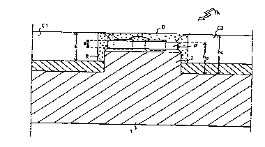
Figures 3a and 3b illustrate such a filling
operation. These figures repeat Figures 2a and 2b with,
in addition, the resin R, shown by black dots. Under
this resin, the concealed constituents, such as the
chip, have been shown as if the resin and the chip were
transparent.
The space in which the chip P lies is limited
laterally only on two sides, by virtue of the printed
circuits C1, C2. It is therefore necessary, before
filling with the resin in the liquid state, to close
the other two sides. This is achieved using a tool
provided with tongs having two jaws Al, A2, which tool
is guided along the edges of the board 1 and of the
printed circuits C1, C2 in order to position its jaws;
since the construction of such a tool or of another
tool or indeed of a mounting capable of fulfilling the
same function lies within the scope of those skilled in
the art of mechanics, in order to simplify the
explanation and therefore to make it clearer only the
two jaws have been shown, in the position they occupy
during filling and during curing of the resin. The jaws
A1 and A2 are mutually parallel plates having a length
barely less than the distance between the two printed
circuits and having a height equal to the thickness E
of the printed circuits. The upper edge of the jaw A1
is identified by the letter D in Figures 3a and 3b.
CA 02305635 2000-03-28
By adjusting the resin level in this way, it is
possible for the thickness for the layer deposited on
an electronic chip to be accurately predetermined
depending on the operating frequencies to be achieved;
thus, in the embodiments which have served as examples
in the present description, it has been possible to
limit the reduction in transmission due to the
encapsulation to less than 0.7 decibels at a frequency
of 40 GHz; for this, it appears that the predetermined
value of he - hp not to be exceeded is 100 micrometres.
Correct implementation of the process that has
just been described requires machining the base and
controlling the solder thicknesses and resin
thicknesses such that the tolerances on the dimensions
are compatible with the predetermined value not to be
exceeded. It also requires choosing an encapsulation
product - resin or other material - which contracts
only very slightly when it solidifies.
This solidification conventionally takes place
at high temperature in an oven and is followed by
removal of the tool fitted with the jaws A1, A2; this
is depicted in Figures 3a, 3b by an arrow marked Th. In
order to compensate, if necessary, for a slight
contraction of the resin on passing through the oven,
it is possible, by taking advantage of the viscosity of
the resin before curing, to meter the supply of resin
so that, without extending beyond the printed circuits
and the jaws, there is a slightly convex surface.
The supply of resin may be metered in various
ways and, in particular: by line of sight; - by a
calibrated drop deposited on the chip by means of a
syringe for example; - by application using a brush;
using a calibrated stencil with a flexible bag which
contains the resin and leaves it to be deposited by
pressure; - by a centrifuge: rapid rotation of the
electronic card allows the resin to be kept only on the
chip; - or indeed by using, instead of the tool with
jaws shown in Figures 3a, 3b, a tool with jaws + cover
so as to form a closed space provided with two
CA 02305635 2000-03-28
orifices, one for injecting the resin and the other for
acting as a vent, that is to say for allowing the
excess resin injected to escape. In the embodiments
that have served as an example in the present
description, the first and then the second ways were
used.
The invention is not limited to the description
above; thus, in particular, instead of forming an
integral part of the base, the tab may be a metal piece
attached to the plate by soldering or with the aid of a
conducting adhesive; Figure 4 illustrates such a base
with a plate 1, a piece T', fastened by a soldered
joint St, being on one of the faces of this plate.
Another possible way of implementing the
process involves a design of electronic cards in which
the printed-circuit part completely surrounds the chip
to be encapsulated. This may be accomplished using four
printed circuits side by side in order to leave on the
plate only the area needed for connection to the chip.
This may also be accomplished, as illustrated in Figure
5, by means of a single printed circuit C, pierced by a
hole Oc, the position and dimensions of which are
determined according to the connection to the chip P.
It should be noted that the alternative methods
of implementing the process which were mentioned in the
previous paragraph make it easier for the chip to be
encapsulated; on the other hand, for cards already
studied, they go beyond a simple modification of the
base and of a possible replacement of two printed
circuits, which is intended to bring these circuits
closer to the chip; these alternative methods are
therefore difficult if they are not provided right from
the design of the electronic card.