Note: Descriptions are shown in the official language in which they were submitted.
CA 02305894 2003-05-20
ELECTRONIC DEVICE STRUCTURE CAPABLE OF PREVENTING MALFUNCTION
CAUSED BY ELECTROMAGNETIC WAVE COMING FROM THE OUTSIDE
This invention relates to an electronic device structure having an electronic
component and a circuit board on which the electronic component is mounted,
and
particularly relates to an electronic device structure having an
electromagnetic shielding
for shielding input/output terminals of an electronic component mounted on a
circuit board
from electromagnetic waves coming from the outside.
Generally, an electronic device such as an IC chip or an LSI chip is packaged
in a PGA (Pin Grid Array) package or a BGA (Ball Grid Array) package having a
plurality
of input/output terminals (i.e. pins or balls) to form an electronic
component. Tree electronic
component is mounted on a circuit board and electrically connected to a
printed circuit
formed on the circuit board.
It is well known that electronic devices may be influenced by electromagnetic
waves coming from the outside. That is, there is likelihood of the electronic
device
malfunctioning when it receives the electromagnetic waves. So the PGA or BGA
package
is normally covered with a metal case or film as an electromagnetic shielding
1:o shield the
electronic device from the electromagnetic waves coming from the outside.
However, the input/output terminals are still exposed and inevitably receive
the electromagnetic waves coming from the outside. Accordingly, there is a
case where
malfunction (or faulty operation) occurs in the electronic device due to the
electromagnetic
waves received with the inputJoutput terminals, even though the metal film
covers the
electronic device.
Moreover, the exposed input/output terminals radiate other electromagnetic
waves caused by an operation of the electronic device. Consequently, there is
a case
where another electronic device located near the electronic component faultily
operates
when it receives the electromagnetic waves radiated from the input/output
terminals.
It is therefore an object of this invention to provide an electronic device
structure which is capable of preventing inputloutput terminals of an
electronic component
mounted on a circuit board from receiving electromagnetic waves coming from
the outside.
It is another object of this invention to provide an electronic device
structure
which is capable of preventing input/output terminals of an electronic
component mounted
-1-
CA 02305894 2003-05-20
on a circuit board from radiating electromagnetic waves caused by an operation
of the
electronic component.
It is still another object of this invention to provide an electronic device
structure which is capable of preventing an electronic component mounted on a
circuit
board from malfunctioning.
It is a further object of this invention to provide an electronic device
structure
which does not radiate electromagnetic waves.
According to the present invention, there is provided an electronic device
unit
comprising: a circuit board having a printed circuit, an electronic component
having a body
and an input/output terminal, wherein the input/out terminal projects from the
body, is
connected to the printed circuit, and supports the electronic component on the
circuit
board, and a first electromagnetic shielding formed on the circuit board for
enclosing the
input/output terminal when the electronic component is mounted on the circuit
board,
wherein the first electromagnetic shielding is located between the circuit
board and the
body mounted on the circuit board.
Further, according to the present invention, there is provided an electronic
device unit comprising: a circuit board having a printed circuit, an
electronic component
having a body and an input/output terminal, wherein the input/output terminal
projects from
the body, is connected to the printed circuit, and supports the electronic
component on the
circuit board, and a first electromagnetic shielding formed on the circuit
board for enclosing
the input/output terminal when the electronic component is mounted on the
circuit board,
wherein the first electromagnetic shielding is made of conductive paste.
Embodiments of the invention will now be described, by way of example, with
reference to the accompanying drawings, in which:
Fig. 1 shows a sectional view of a conventional electronic component having
a semiconductor device packaged in a BGA package;
Fig. 2 shows a sectional view of an electronic device structure according to
a first embodiment of this invention;
Fig. 3 shows a perspective view of a high dam of Fig. 2;
Fig. 4 shows a perspective view of a metal mask for forming the high dam of
Fig. 2;
-2-
CA 02305894 2003-05-20
Fig. 5 shows a sectional view for describing a method offorming the high dam
of Fig. 2;
Fig. 6 shows a sectional view of an electronic device structure according to
a second embodiment of this invention; and
Fig. 7 shows a sectional view of an electronic device structure according to
a third embodiment of this invention.
Referring to Fig. 1, description will be at first directed to a conventional
electronic component for a better understanding of this invention.
In Fig. 1, the conventional electronic component 10 has a semiconductor
device 11 such as an IC chip, an LSI chip, etc., and a BGA (Ball Grid Array)
package for
packaging the semiconductor device 11.
The BGA package comprises a base 12 on which the semiconductor device
11 is mounted. Printed wiring 13 is formed on both upper and lower surfaces of
the base
12. Metal wires 14 connect the semiconductor device 11 to the printed wiring
13 at the
upper surface of the base 12 when the semiconductor device chip 11 is mounted
on the
upper surface of the base 12. A resinous seal 15 is formed on the upper
surface of the
base 12 to seal the semiconductor device 11 together with the metal wires 14.
Solder balls
16 are formed on the printed wiring 13 at the lower surface of the base 12.
The solder
balls 16 are used for input/output terminals of the electronic component 10. A
metal film
17 as an electromagnetic shielding covers the whole outside surface of the
electronic
component 10 except for exposed parts of the printed wiring 13 and the solder
balls 16.
Additionally, the metal film 17 is isolated from the printed wiring 13.
The metal film 17 prevents electromagnetic waves coming from the outside
from impinging on the semiconductor device 11. That is, the metal film 17
prevents
malfunction caused by the electromagnetic waves in the semiconductor device
11.
Such an electronic component is disclosed in Japanese l~nexamined
Japanese Patent Publication (JP-A), No. H8-288686.
However, the conventional electronic component suffers from the drawback
that the solder balls 16 are exposed to the atmosphere and inevitably receive
electromagnetic waves. The electromagnetic waves received by the solder balls
16 are
transmitted to the semiconductor device 11 through the printed wiring 13 and
tend to cause
malfunction of the semiconductor device 11.
-3-
CA 02305894 2003-05-20
Moreover, there is a case that the solder balls 16 radiate electromagnetic
waves caused by an operation of the electronic device chip 11. The
electromagnetic
waves radiated from the solder balls 16 causes faulty operations to
neighboring devices.
Particularly, with increase of operation speed of the electronic device 11,
influences of the
electromagnetic wave radiated from the solder balls 16 becomes large.
Referring to Figs. 2 through 5, the description will proceed to an electronic
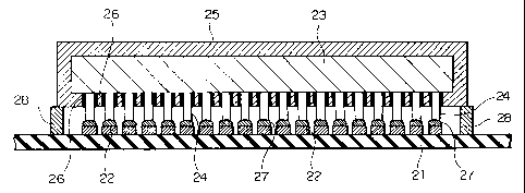
device structure according to a first embodiment of this invention.
In Fig. 2, the electronic device structure comprises a circuit board 21 having
a printed circuit which includes a plurality of contact pads 22 formed on an
upper surface
of the circuit board 21. An electronic component 23 has a body including an
electronic
device (not shown) and a plurality of input/output terminals 24 protruded from
the body.
A metal case 25 covers the body of the electronic component 23 except for
neighborhood
of each of the inputloutput terminals 24. Insulators 26 are placed between the
metal case
25 and the input/output terminals 24 to insulate the inputloutput terminals
from the metal
case 25. The electronic component 23 is mounted on the circuit board 21 and
the
input/output terminals 24 are connected to the contact pads 22, respectively,
by soft solder
27. A high dam 28 is formed on the upper surface of the circuit board 21 as an
electromagnetic shielding so as to enclose the input/output terminals 24 and
so as to keep
contact with a lower surface of the metal case 25 mounted on the circuit board
21 at its
top. The high dam 28 has a square frame shape corresponding to a shape of the
electronic component 23 as shown in Fig. 3.
The high dam 28 is formed by, for example, a screen printing method using
a metal mask such as shown in Fig. 4 and solder paste. The solder paste has
strong
adhesive strength and is readily available at a low price. In addition, the
solder paste
works easily.
In Fig. 4, the metal mask 41 has a thickness corresponding to the height of
the high dam 28 and has openings or apertures 42 which are continuous with one
another
at the rear side of the metal mask 41 so as to correspond to the shape of the
high dam 28.
That is, the metal mask 41 has an outer frame 43 and a middle plate 44
connected to the
outer frame 43 with thin beams 45.
In the screen printing method, the metal mask 41 is put on the upper surface
of the circuit board 21 as illustrated in Fig. 5. Then, solder paste 51, which
is conductive
CA 02305894 2003-05-20
material, is put on the metal mask 41 and pushed by a squeegee 52 (i.e. a
rubber spatula)
along to an arrow A. As a result, the solder paste 51 rolls on the metal mask
41 (as shown
by an arrow B) and is squeezed into the openings 42 with the squeegee 52.
Because the
solder paste 51 is soft, it easily spreads over the upper surface of the
circuit board 21 and
into the openings 42. Next, the solder paste 51 is heated and hardened. After
the solder
paste 51 is hardened, the metal mask 41 is taken away from the surface of the
circuit
board 21. Thus the high dam 28 is formed on the circuit board 21.
Additionally, the contact pads 22 may be formed by the screen method
together with the high dam 28. In this case, the metal mask 41 has two areas
which are
different from each other in thickness so as to make a difference in height
between the
contact pads 22 and the high dam 28.
Returning to Fig. 2, the metal case 25 shields the body of the electronic
component 23 from electromagnetic waves coming from the outside. On the
contrary, the
metal case 25 prevents electromagnetic waves from radiating from the body of
the
electronic component 23 to the outside. Similarly, the high dam 28 shields the
input/output
terminals 24 from the electromagnetic waves coming from the outside and
prevents
electromagnetic waves from radiating from the input/output terminals 24 to the
outside.
The metal case 25 and the high dam 28 transform the electromagnetic waves
incident on them into electric current. The electric current is transformed
into heat or flows
to the ground through a ground wire (not shown) on the circuit board 21.
Because the metal case 25 and the high dam 28 shield the electronic
component 23 as mentioned above, faulty operation or malfunction is not caused
in the
electronic component 23 by the electromagnetic waves coming from the outside.
Furthermore, because electromagnetic waves generated by the electronic
component 23
do not escape to the outside, neighboring devices (not shown) located near the
electronic
component 23 do not malfunction.
Referring to Fig. 6, an electronic device structure according to a second
embodiment of this invention will be described. The electronic device
structure is similar
to the electronic device structure illustrated in Fig. 2, except for a high
dam 61.
In Fig. 6, the high dam 61 is formed on the circuit board 21 so as to enclose
not only the input/output terminals 24 but also under part of the metal case
25. An inner
-5-
CA 02305894 2003-05-20
wall of the high dam 61 is in contact with a side surface of the metal case
25. It is possible
that there is no space between the metal case and the high dam 61.
The high dam 61 shields not only the input/output terminals 24 but also a part
of the body of the electronic component 23 from the electromagnetic waves.
Accordingly,
it is more difficult for electromagnetic waves coming from the outside to
impinge upon the
electronic component 23.
Referring to Fig. 7, an electronic device structure according to a third
embodiment of this invention will be described. The electronic device
structure is similar
to the electronic device structure illustrated in Fig. 2 except for a circuit
board 71 and the
length of the input/output terminals 24.
In Fig. 7, the circuit board 71 has a plurality of through holes 72 for
receiving
the input/output terminals 24. The input/output terminals 24 are inserted into
the through
holes 72, respectively, and connected to the printed circuit 73 by soft solder
74 at the lower
surface of the circuit board 71.
In this structure, the high dam 28 prevents the electronic companent 23 and
the metal case 25 from bumping on the circuit board 71 when the electronic
component
23 is put on the circuit board 71. Moreover, the high dam 28 prevents the
metal case 25
from electrically connecting with the printed circuit on the circuit board 71.
While this invention has thus far been described in conjunction with preferred
embodiments thereof, it will readily be possible for those skilled in the art
to put this
invention into practice in various other manners. For example, the high dam
may be made
of (a) other metals) or a magnetic body. Moreover, the high dam may be of
other shapes.
Moreover, the input/output terminals may be a ball type ar other types.
-6-