Note: Descriptions are shown in the official language in which they were submitted.
CA 02306072 2000-04-14
1
Down Converter and Demodulator using_a Three port function
Field of the Invention
The present invention relates to a down converter for RF signals, a
demodulator
comprising a down converter, a mobile communications device comprising such a
demodulator, a method for down converting RF signals by means of one three
port
junction as well as to a demodulation method.
Background of the Invention
The proposed technique is particularly convenient for down converting and
demodulating RF signals modulated with a modulation scheme with constant
envelope
such as f.e. nPSK (Phase Shift Keying).
The so-called six-port technology which has been used up to the last years for
complex
measurements can also be utilised for designing receivers. Receiver built on
the basis of
a six-port assembly act in the direct conversion manner allowing therefore a
conversion
from for example signals in the mm-wave range and microwave range directly to
a base
band frequency. The main feature of the six-port receiver thereby is the
detection of the
vector ratio between two incoming vector signals by means of a power sensing
at
different positions within the RF circuitry of the six-port topology. A direct
six-port
receiver is for example described in Ji Li, R. G. Bossisio and Ke Wu: "A six
port direct
digital millimetre wave receiver", Digest of IEEE MTT Symposium, voL3, pp 1659-
1662, San Diego, May 1994.
From the W099/08426 a non-coherent six-port receiver is known. This known
receiver
comprises a power divider to divide a modulated RF input signal in at least
two
branches. At least one delay line provides for a delay of the branches
relatively to each
other by a predetermined delay constant. A calculation circuit calculates at
least three
power levels based on combinations of the two branches of the input signal
relatively
delayed to each other. A processing means calculates the phase and the
amplitude of a
CA 02306072 2000-04-14
2
complex signal representing the relation between the two branches of the input
signal
relatively delayed to each other, on the basis of the said at least three
power levels.
Summary of the Invention
It is the object of the present invention to further develop the above-cited
non-coherent
six-port receiver technology such that the complexity of the necessary
circuitry can be
reduced.
This object is achieved by means of the features of the independent claims.
The
depending claims developed further the central idea of the present invention.
The new technology according to the present invention allows the same
functionality as
a non-coherent six-port receiver topology as it is set forth in the
W099/08426.
However, the RF circuitry can be significantly reduced and only two power
sensors are
necessary. A local oscillator can be omitted. In case of simple modulation
techniques
like (n) PSK there is furthermore no need for a RF switch.
According to a first aspect of the present invention therefore a down
converter for RF
signals is provided, wherein the down converter comprises one three port
junction
device. The three port junction device has one input port and two output
ports, wherein
the output ports are respectively connected to a power sensor.
The down converter can be a non-coherent down converter without any local
oscillator.
The three port junction device can comprise a power splitter dividing the
signal supplied
to the input terminal into two branches. Furthermore a processing means for
processing
one of the branches and a four port junction device for combining the two
branches and
for generating two output signals to be supplied to the output terminals are
comprised in
the three port junction device.
The processing means can comprise a delay unit.
Alternatively the. processing means can comprise a frequency divider, at least
one filter
means and a frequency multiplier.
CA 02306072 2000-04-14
3
The dividing factor of the frequency divider is equal to the multiplying
factor of the
frequency multiplier.
A switch can be provided in the signal branch processed by the processing
means.
According to the present invention furthermore a demodulator comprising a down
converter as set forth above is provided. The signal supplied to the input
port in this
case is a digital modulated signal and the switch is controlled to be opened
during a
time duration corresponding to one half of the bit duration of the supplied
digital
modulated signal.
Respectively one AID converter can be connected directly or indirectly with
one of the
power sensor.
According to another aspect of the present invention a demodulator comprising
a down
converter as set forth above is provided. At least one averaging unit is
connected
directly or indirectly with the output of the power sensor and the output of
the
averaging units is supplied together with signals corresponding to the input
signal of the
at least one averaging unit to at least one analog processing unit.
According to the present invention furthermore a mobile communications device
comprising a demodulator as set forth above is provided.
According to a still further aspect of the present invention a method for down
converting RF signals by means of one three port junction device is provided.
A RF
signal is supplied to one input port of the three port junction device. Two
output signals
are generated on the basis of the one input RF signal. The output signals are
supplied at
two output ports of the three port junction device respectively to a power
sensor.
3fl
The step of generating two output signals on the basis of the input RF signal
can
comprise the step of dividing the signal supply to the input terminal to two
branches.
One of the branches is processed and the two branches are combined, wherein as
a
CA 02306072 2000-04-14
4
,,
result of the combination of the two branches two output signals to be
supplied to the
output terminals and thus to the power sensors are generated.
The step of processing one of the branches can comprise the step of delaying
the signal
of the corresponding branch by a time duration corresponding to the time
duration of at
least one modulation bit of the input RF signal.
The step of processing one of the branches alternatively can comprise the
steps of
frequency dividing, filtering and frequency multiplying the signal of the
processed
branch.
The dividing factor of the frequency dividing step is equal to the multiplying
factor of
the frequency multiplying step.
The processed signal branch can be optionally switched on and off.
According to a still further aspect of the present invention a demodulating
method is
provided comprising the steps of the down-converting method as set forth
above. In this
case the signal supply to the input port of the three port junction device is
a digital
modulated signal and the switching is controlled to be opened during a time
duration
corresponding to one half of the bit duration of the supplied signal.
The demodulating method can comprise the step of AID converting at least one
signal
based on output signals of the power sensors.
The demodulating method can comprise a down-converting method as set forth
above
and furthermore is still a step of averaging the output of at least one of the
power
sensors and analog processing the output of the averaging step and signals
corresponding to the input signal of the averaging step.
More than one demodulation state can be generated by the analog processing
step, such
that additional information is obtained indicating the quality of the
demodulation. This
(soft) information can be used in a decoding step.
CA 02306072 2000-04-14
w
The demodulating method can comprise the steps of AID converting the output of
the
analog processing step with more than two bits, digitally processing the AID
converted
signals and supplying the digitally processed signals to a soft decision unit.
5 Brief Description of the Drawin",gs
Further advantages, features and objects of the present invention will now be
explained
with reference to a plurality of embodiments of the present invention and by
referencing
to the figures of the enclosed drawings.
Fig. 1 shows a schematic diagram of the general structure of a down
converter according to the present invention,
Fig. 2 shows the internal structure of a linear three port circuitry
according to the first embodiment of the present invention,
Fig. 3 shows a second embodiment for the internal structure of the linear
three port circuitry according to the present invention,
Fig. 4 shows a functional description of am ideal four port junction
device used in the linear three port circuits according to the embodiments
- of fig. 2 and 3, respectively,
Fig. 5 shows a possible implementation of a four port junction device
with an isolation function,
Fig. 6 a, b show further possible implementations for a four port junction
device using resistive elements,
Fig. 7 shows the circuitry attached to the DC interface of fig. 1,
Fig. 8 shows a further possible option for the circuitry attached to the DC
interface,
CA 02306072 2000-04-14
6
Fig. 9 shows a still further possible option of the circuitry attached to the
DC interface,
Fig. 10 shows a still further option of the circuitry attached to the DC
interface of Fig. 1,
Fig. l la shows the internal structure of the power sensor bloc according
to the present invention,
Fig. l lb shows differential or not differential QPSK states demodulated
by the down converters on the basis of fig. 3 and 2, respectively, with a
SIN ratio of 9dB,
Fig. 12 shows differential or not differential 8PSK states demodulated by
the down converters according to fig. 3 and 2, respectively, in case of a
SIN ratio of lSdB,
Fig. 13 shows the ideal DC output of the power sensors,
Fig. 14 shows ideal DC output signals of the power sensors with a signal
to a noise ratio of 9dB,
Fig. 15 shows ideal DC output signals of the power sensors without
noise,
Fig. 16 shows ideal DC output signals of the power sensors in the case of
a signal to noise ratio of lSdB,
Fig. 17 shows ideal DC output signals of the power sensors without
noise.
CA 02306072 2000-04-14
Detailed Description of the Preferred Embodiments
The present inventions is particularly applicable to direct receivers for
applications
where mostly one channel communication is targeted. The proposed technology is
particularly suitable for demodulation and down-conversion of PSK modulation
or
. generally phase state modulation, according to which the magnitude of the
signals are
constant due to the modulation process. In case of such an operation no local
oscillator
signal is needed. Method of the down-conversion based on the proposed
technology will
be described and simulations will be explained later on.
The proposed receivers using six-port technology usually utilized four power
sensors.
According to the central idea of the present invention only two power sensors
are used
without time multiplexing. Local oscillator signals are not needed.
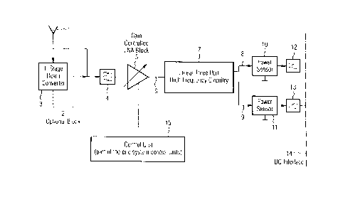
With reference to fig. 1 a down-converting receiver comprising a linear three
port
circuitry 7 will now be explained. A digital modulated RF signal is received
by an
antenna 1. Optionally a block 2 comprising a first stage down converter 3 can
be
provided. The antenna signal and the output signal of the optional block 2,
respectively,
are passed through a band pass filter 4 and then amplified by a low-noise
amplifier ~.
The gain of the LNA amplifier ~ is controlled by control unit 15 which is part
of the
system control unit. The output signal of the LNA 5 is input to the only one
input
terminal 6 of the linear three port device 7. The linear three port device 7
has two
output terminals 8, 9, at which output signals generated on the basis of the
signal
supply to the input terminal 6 are supplied to power sensors 10, 11. The
output signals
of the power sensors 10, l I are low-pass filtered 12, 13 and then supplied to
a DC
interface 14. The circuitry connected on the other side of the DC interface 14
will be
explained later on.
As can be seen from fig. 1, the down converter essentially consists of a
passively near
three port high frequency circuitry 7 having one input terminal 6 for
modulated RF
signals and two RF outputs 8, 9 connected to the two power sensors 10, 11.
With reference to fig. 2 and 3 different embodiments of the internal structure
of the
three port junction device 7 will now be explained.
CA 02306072 2000-04-14
8
According to the embodiment of fig. 2 the signal supplied to the input
terminal 6 of the
three port junction 7 is split by a power divider 16 into a first and a second
branch. The
first branch (RF signal 1) is supplied directly to a four port junction device
20.
The internal structure and the functionality of a four port junction device is
known from
PCTIEP 98 083 29 in the name of Sony International (Europe) GmbH. As the four
port
junction device is explicitly explained in that application, a detailed
description of a
four port junction device in the frame of the present description is omitted
and reference
is made to the corresponding figures and parts of the description of PCT/EP 98
083 29.
The second branch generated by the power divider I6 is optionally supplied to
a switch
17 or directly supplied to a delay line 18. The delay line 18 provides for a
delay
corresponding to the time duration of vne or more modulation bits of the
digital
modulated RF signal supplied at the input terminal 6. The output signal of the
delay line
18 is amplified 19 and supplied as RF signal 2 to the second input terminal of
the four
port junction device 20. The output signals supplied to the power sensor 10,
11 are
generated at the output terminals of the four port junction device 20.
According to the embodiment of fig. 2 therefore the linear three port passive
circuitry 7
contains a power sputter (power divider) 16 for splitting the incoming RF
signal into
two branches. One branch is directly supplied to the four port junction device
20 and
the second branch is processed either as shown in fig. 2 or as shown in fig. 3
as will be
explained later on. Optionally the signal of the first branch can be passed
through an
isolation unit 49 before being supplied to the four port junction device 20.
According to the embodiment of fig. 2 the second branch generated by the power
splitter 16 is delayed by a duration of one (or several) modulation bits by
the delay line
18. For the implementation of the RF delay line 18 several implementations are
possible. After the optional amplification by the amplifier 19, which serves
for a
possible correction of the delay line losses and for an isolation, this signal
(RF signal 2)
is supplied to the four port junction device 20. It is to be noted that the
amplification
CA 02306072 2000-04-14
9
can take place before or after the delay line 18. The amplifier gain can be
set to one, in
which case the amplifier 19 purely serves as isolation unit.
Now the second embodiment for processing the second branch of the RF signal
generated by the power splitter 16 will be explained. After optional being
passed
through the switch I7, the signal in the second branch is supplied to a
frequency divider
21 having a dividing factor N. The output signal of the frequency divider 21
is passed
through a filter 22 and then to a frequency multiplier 23 having a multiplying
factor
preferably equal to the frequency division factor N. The output signal of the
frequency
multiplier 23 is again passed through a filter 24, amplified by the amplifier
19 and then
supplied to the second input terminal of the four port junction device 20 as
RF signal 2.
Again it is to be noted that the low-noise amplification by the amplifier 19
can take
place in any position of the second branch. Furthermore it is to be noted that
the
frequency division factor and the multiplying factor can be chosen arbitrary,
but
preferably a factor of two is enough. Due to this processing of the RF signal
in the
second branch as shown in fig. 3, the phase information contained in the
signal is lost.
The optional switch can be particularly omitted in case a simple modulation
technique
like (n) PSK is~ used and the general conditions do not vary too much in time.
Optionally an isolation unit 49 may be provided in the first branch between
the power
splitter 16 and the four port junction device 20.
Reference is now made to fig. 4 showing a mathematical description of the
ideal four
port junction device 20 using the S-matrix approach. A plurality of different
implementations can be used to realize the functionality described by the S-
matrix of
fig. 4. Fig. 5 and fig. 6 show two possible implementation options for a four
port
junction device. Note that a detailed description of the four port junction
device is again
omitted as four port junction devices are already explained in detail in the
application
PCT/EP/98/083 29 as set forth above.
As can be seen in fig. 5, according to this implementation, a first RF signal
1 is
supplied to a first power splitter 25 and a second RF signal 2 is supplied to
a second
power splitter 26. The power splitter 25 and the power splitter 26 are
connected to a
CA 02306072 2000-04-14
~ 10
hybrid circuit 28 which is connected to earth by a termination 30 and which is
furthermore connected to the interface to the power sensor 1. The second
signal
branches respectively generated by the power splitter 25 and the power
splitter 26 are
supplied to a second hybrid circuit 29, wherein the second branch signal
generated by
the second power splitter 26 is first phase shifted by a phase shifter 27
before being
supplied to the hybrid circuit 29. The second hybrid circuit 29 again is
connected to
ground by a termination circuit 31 and with an interface to the power sensor
2. Note
that also 90° and 180° hybrids may be used and the function of
the circuitry is
explained in the application PCTIEPI98/083 29.
Fig. 6 shows a further possible implementation for a four port junction device
in the
case that an isolation function is obtained by other external means. A
detailed
description of the,implementation is shown in fig. 6 can also be found in the
application
PCTIEP98I083 29.
In the following equations (1) to (23) a general mathematical description of
the
proposed down conversion method. For both cases of the Fig. 2 and Fig. 3 the
applied
mathematical description is similar. Mathematical presentation is shown for
case of the
Fig. 3, having related time delay functionality.
Table 1 shows the legend of the used variables.
vt = p Vaeiw C1)
~, = vo C2?
y = peiw (3)
1 =pcos~ ~,3=psincp
vZ
CA 02306072 2000-04-14
11
Equation e four
S presents pore
the junction.
ideal
S nacrix
or
th
0 ~ 51) 51a 0 s13 51.t
0
- O O s~ S~ O O s,3 sz<
szZ 0 0 kJ~eie,~ 0 0 (4)
~Ze;ez
say ke' k:ze'e''0 0
.saz
O O
~t = (5)
S"vnf'
Szz"Z
= kJ,e'',~
pe;wv,
y k3=e,e"
v~
v< = (6)
saiv~
+ r~v2
= k~~e%~'~
pewvz
+ k<Ze~u"
~_
e,~ (~)
:
v3 -
(koPe~(e"
~~
e~:
T~?
T kiz
)~
-
~4 =
(ka'pe;ie"-et (8)
.,,~
y k
e;e"
a
_
p~ = ~))
p_~k3~P~
~-k
i +Zk"k3zPcos(6;,
-8,z
+
p.~ cP)~ (10)
= p,
(k
ip=
~ ku
+ 2k<ikd,pcos(8<,
- 6<z
+
p~=N~P, (I1)
f
P
3 ( 12)
f'z
=
--
~
W ~
~'
k
k
~
.n
(13)
X1 = k''--P- ~ k3? p_~ _ ki~P- - k i
z ; z ~
2kz~k~z pz 2kz~k3z 2kokai
k3tP= pJ - ka,P~ (14~)
X' -
<
Zk"k~ P, 2ka'k< -'~
k
2 m
83~ e,z ~6a = 6<, - 8
~', = p cos(a8s .;- ~) _~ p(cos ~6, cos c~ - sin X83 ( I 6)
sin c~ ~
3C ,~< = p(cos ~s< T ~) = p~cos~A, cos c~ - sin a.6<
sin ~~
CA 02306072 2000-04-14
12
X, sin a8, - X, sin ~6~
I=
si~(08, -D8~)
_ X~ cosd8a - X, cOS~6, (I9)
sin(G8, - Q83)
(20j
~9~ :. k 2 , ~9; ~ k 2 , 08, - d6, : krt
Y = 1 - X, Sln.De, - X~~sII1 ~6~ . (21)
i
p ø sin(~8, = ~6~ ) . _ .
Yz = sgn(Q) . (?
cp = YZ arccos(Y ) . (23)
v, RF si anal to be I/Q demodulated
Second R.F signal (known)
. ( magnitude ratio between RF signal one and two
phase difference betureen RF signal one and tzvo
S S ma.triz of the four on 'unction
__ma itude of the tom lex transfer function from ort n to
m
2oi6,~n phase of the complex transfer function from port n to m
v3 ~ si aI which a roaches ower sensor 1 _
signal which a roaches over sensor 2 .
Power level detected at ower sensor 1
Power level detected at ower sensor 2
P, Averaged Power level detected at power sensor 1 after N signals
X~ ~ Hel -function of Power P3
Hel -function of Power P
Normali2ed I value to be converted in the digital domain
~ Sign of Q value
Table 1. Legend of used variables
CA 02306072 2000-04-14
w I3
The major impact is that the signals before approaching four port junction 20,
(of the
Fig. 2 and Fig. 3) contain two different noise portions. That also means that
proposed
non-coherent system has larger noise sensitivity compered to the coherent
solution, but
potentially simpler realisation. The advantage of the simple realisation is
growing with
the increase of the frequency of operation.
With reference to Fig.l now different implementations of circuitries connect
to the DC
interface 14 will be explained. As shown in Fig. 7 the DC interface 14 can be
connected by means of two AID converting means 32, 33 to a digital processing
unit
(DSP unit) 34 and a demodulation unit 35. The DSP unit 34 is in charge of
processing
the incoming digital signals either to effect an demodulation or even a full
signal
demodulation. Note that the control unit 15 which is part of the system
control units can
be designed to control the AID converter 32, 33 as well as the digital
processing unit
34.
Fig. 8 to 10 show other implementations having two DC inputs coming from the
power
sensors 10, 11 after being filtered in the filters 12, 13. Furthermore
according to the
implementations of Fig. 8 to 10 two DC outputs are provided which are
connected to
analogue processing and averaging units. Optionally an additional Iow-pass
filtering can
be applied.
Method of Operation in the case of the (n) PSK demodulation
Figures, 8,9 and 10 are related to the (n) PSK demodulation using the concept
according to the present invention. In all three figures three different
options for analog
circuits realization are proposed. The whole signal information is placed in
the relative
phase of the modulated signals. According to this fact information about
signal
magnitude does not necessarily contain the information. This means that only
two
power sensors are enough to decode the signals, taking into account the non-
coherent
operation proposed.
CA 02306072 2000-04-14
14
Moreover using the method according to the present invention, the requirements
of the
gain control may be reduced, meaning that digital gain control may be omitted,
and
only simple analog rough gain control may be sufficient. The detected DC
levels at the
power sensors outputs are averaged in an analogue manner and supplied to the
two
analog processing entities 36, 37 (Figures 8 and 9). Averaging is done over
more
symbols. Timing information comes from the control unit 15. The averaged
values on
both power sensors 10, 11 determine thresholds, which are used for analog
comparison
and hard decision, according to the following equation.
Taking into account the embodiments of Fig. 2 to 6 it is obvious that the
transfer
functions (from RF signal inputs to the related power sensors) of the four
port junction
are also known, as well as related phase shift. That means that thresholds for
nPSK
can be calculated, having only information of the average power. Thresholds
for QPSK
are straight forward. Information about thresholds is further provided to the
analog
15 circuitry 38 giving hard-decision (n) PSK demodulated values (Fig. 8). By
the usage of
the analog circuitry 38 it is possible to perform hard decision demodulation,
which has
additional information, which may be useful for channel decoding entity.
Namely, if
the signal/noise ratio decreases, there might occur the case that the hard
decision block
38 denotes more than one demodulation states. This may be also understand as
some art
20 of the additional "quasi soft bit" information.
In Fig. 9 instead of the single "Analog circuitry block" two 2-4 bits AID
converters 40,
41 are provided giving "quasi soft bits. The term "Quasi" means that obtained
bits have
to be further DSP processed before provided to a decoding unit, which support
soft bits
operation. That also means that this part of the digital processing may be
incorporated
by ASICs directly, at the input of the decoding entity.
Method and apparatus of operation in the case of the phase demodulation, where
magnitudes of signal are constant
The devices required for this operation are described at the Fig. 10, which
are attached
to the structures of the Fig. 2 or Fig. 3, and it can be named phase
demodulator. At the
DC interface 14, at (at least one) power sensor, an analog unit 36, 37 for
signal
CA 02306072 2000-04-14
1$
averaging is attached connected to the analog circuitry 38 which is defined
according to
the above equations. The result of the analog processing are normalized I
values and
signum function of the Q value, which are provided to the two AID converters
40, 41,
where one of them is one bit converter at it is attached to the signum
function unit 42.
After obtaining cosine value of the phase difference and signum value, after
digitizing,
further digital processing 43 may be performed to calculate the actual values
of the
phase information.
Fig. l la show the internal structure of a power sensor 10, 11. The central
part of the
power sensor is a detector diode, a temperature power sensor and a FET
structure 44.
Furthermore an optional matching network 45, an optional biasing unit 46 and
an
optional analog compensation hardware for non-linear behaviour 47 is connected
to the
central unit 44. Note that a detailed description of the function and the
internal structure
of a power sensor can be found in PCT/EP98/083 29.
With reference to Fig. l ld to 17 now simulation results will be explained.
This
simulation has been performed to verify the proposed technology and
particularly to
verify the proposed technique under the following simulation conditions:
-the power sensors are detector diodes which are working in the linear region
and have
an input impedance with the same tolerances (reactive part considered as
matched) as
the discrete resistors in the assembly,
-the three port junction is realized by the resistive elements as shown in
Fig. 6 taking
into account the general topology of Fig. 3. The delay process is considered
as being
ideal, and
-the resistor absolute values are considered having tolerances of 0% and 1~ %
Fig. l lb show differential and non-differential QPSK states demodulated by
the
structures of Fig. 3 and 2, respectively, with a signal/noise ratio of 9dB.
CA 02306072 2000-04-14
16
I shows QPSK signals with a noise margin in case of an ideal four port
junction and a
demodulation with an external local oscillator signal,
II shows as a comparison to the present invention, QPSK signals with a noise
margin
for a real four port structure, wherein absolute resistor tolerances of 20 %
are included
and a local oscillator is applied,
III shows QPSK signals with a noise margin for an ideal four port junction
according to
the present invention as shown in Fig. 2 and 3, and
IV shows QPSK signals with a noise margin with a real four port structure
according to
the present invention, wherein resistor tolerances of 20% are included.
Fig. 12 shows differential or non-differential 8PSK states demodulated by the
structures
of Fig. 3 and Fig. 2, respectively, with a signal/noise ratio of lSdB.
I shows 8PSK signals with a noise margin for an ideal four port junction and a
demodulation with an external LO signal (as a comparison to the present
invention).
II shows BPSK signals with a noise margin with a real four port structure of
Fig. 3,
wherein absolute resistor tolerances of 20 %a are included.
III shows 8PSK signals with a noise margin with an ideal four port j unction
according
to the present invention as shown in Fig. 2 and Fig. 3, and
IV shows 8PSK signals with a noise margin that the real four port structure
according
to the present invention, wherein absolute resistor tolerances of 20% are
assumed.
Note that the cases III and IV according to the present invention respectively
show a
lower performance in comparison to the cases I and II, but this is more than
compensated by the simpler design as a local oscillator is no longer
necessary.
Fig. 13 shows ideal DC output signals of the power sensors without noise and
with an
ideal four port circuitry, wherein the output signals are depicted as a
function of the
phase difference of the incoming signals at the input pons of the four port
junction of
Fig. 2 and Fig. 3. The solid Lines show an average value and docket lines show
the
related states. It is assumed that the phase shifter of Fig. 6 has a shifting
value of ~5°.
Fig. 14 shows an ideal DC output of the power sensors with a signal/noise
ratio of 9dB
and with an ideal four port circuitry. The ideal DC outputs are depicted as a
function of
CA 02306072 2000-04-14
17
the phase difference of the incoming QPSK signals at the input ports of the
four port
j unction of Fig. 2 and Fig. 3. The solid lines show the average value and
docket lines
show the related states. It is again assumed that the phase shifter of Fig. 6
has a shifting
value of 45°.
Fig. 15 shows ideal DC output signals of the power sensors without noise and
with an
ideal four port circuitry. The ideal DC output has a function of the phase
difference of
the incoming 8PSK signals at the input ports of the four port junction of Fig.
2 and 3.
The solid lines show average values and the docket lines show the related
states. It is
assumed that the phase shifter Fig. 6 has a shifting value of 45°.
Fig. 16 shows ideal DC output signals of the power sensors with a signal/noise
ratio of
lSdB and to an ideal four port circuitry. The ideal DC output signals are
shown as a
function of the phase difference of the incoming SPSK signals at the input
ports of the
four port junction of Fig. 2 and 3. The solid line shows the average value and
docket
lines show the related states. Again it is assumed that the phase shifter
provides for a
shifting of 45°.
Fig. 17 shows the ideal DC output signals of the power sensors without noise
and with
an ideal four port circuitry, wherein the output is shown as a function of the
phase
difference of the incoming 8PSK signals at the input ports of the four port
junction of
the Fig. 2 and 3. The solid lines show an average value and
the docket line show the related states. It is assumed that the phase shifter
of Fig. 6
provides for a phase shifting value of 75°. Note that the thresholds
are changing with
the change of the phase shift in comparison to Fig. 15 for example. If the
device is
designed to work at a frequency f-index 0 it may also work at a frequency f
index 1 =
f-index 0 x 75/45=f-index 0 x 1.66 (Note the phase shifter is usually linearly
dependent
of the applied frequency). However, as can be seen from Fig. 17, the
thresholds are
closer so that the system would require a better signal/noise ratio if it is
used for
broadband applications.
The present invention proposes a three port technology which allows the same
functionality as known six port receiver topologies but with significantly
reduced RF
CA 02306072 2000-04-14
18
circuitry, having only two power sensors and no need for a local oscillator
(non-
coherent detection). In case of simple modulation procedures like PSK no RFs
which is
needed. The proposed technology addresses cases where only one channel low-
range
communication is targeted. This is quite practical for application where
higher
microwave and lower millimetre-wave range is used and where full Frequency re-
use of
- the one channel may be proposed. This is particularly convenient for simple
modulation
schemes like nPSK. The proposed concept is particularly advantageous for low-
cost
device applications. The proposed solution is furthermore very advantageous
for typical
applications in the millimetre-wave range. Furthermore it is advantageous for
one
channel communication with a simple modulation scheme like QPSK. This might be
particularly interesting for 60 Ghz or 24 Ghz (ISM band) applications.