Note: Descriptions are shown in the official language in which they were submitted.
CA 02306212 2000-04-14
WO 99/19912 PCT/US98IZ1812
- 1 -
DUAIwB~IND QUANTA TiiELI~ IN8'RARED SENSING ARRlIY
O~T~T~1 OF THE INVENT
The invention described herein was made in the
performance of work under a NASA contract, and is subject
to the provisions of Public Law 96-517 (35 U.S.C. 202) in
which the Contractor has elected to retain title.
~'h'~T:O O~' THE INVE'~NTI4N
The present invention relates to radiation
detection and devices thereof, and more specifically, to
a quantum-well radiation sensing array.
8i ~C6ROOND
Quantum-well semiconductor devices can be
configured to detect radiation with improved performance
compared to many other types of radiation detectors.
Unique properties of the quantum-well structures allow
for a high quantum efficiency, a low dark current,
compact size and other advantages.
In particular, various quantum-well structures can
be formed by artificially varying the compositions of
lattice matched semiconductor materials to cover a wide
range of wavelengths in infrared ("IR") detection and
sensing. An intraband transition, that is,
photoexcitation of a carrier (i.e., an electron or a
hole) between a ground state and an excited state in the
same band (i.e., a conduction band or a valance band),
can be advantageously used to detect radiation with a
high responsivity in the IR range at a selected
wavelength by using a proper quantum-well structure
CA 02306212 2003-03-05
- 2 -
biased at a proper voltage. For example, the absorption
wavelength of a quantum-well structure formed of
Al~Gai_,,As/GaAs can be changed by altering the molar ratio
x (0<_ x <_I) of aluminum or the thickness of GaAs layer.
Other materials for infrared detection include Hgl_XCd,Te
and Pb~_vSn,_Te. See, for example, Gunapala and Bandara,
"Recent Developments in Quantum-Well Infrared
Photodetectors," Physics of Thin Films, Vol. 21, pp. 113-
237, Academic Press (1995),
Infrared sensing arrays formed of quantum-well
structures are desirable due to their applications in
right vision, navigation, flight control, environmental
monitoring (e.g., pollutants in atmosphere) and other _
fields. Many conventional infrared arrays respond to
radiation only in a specified wavelength range, such as a
short-wavelength infrared range ("SMIP,") from about 1 to
about 3 um, a mid-wavelength infrared range ("MWIR") from
about 3 to about 5 pm, a long-wavelength infrared range
("LWIR") from about 8 to about 12 pm, or a very-long-
wavelength infrared~range ("VLWIR") that is greater than
about 12 ~Zm. All sensing pixels in a quantum-well
sensing array operating at a specified radiation
wavelength are biased at a predetermined voltage. A
readout multiplexer having an array of readout pixels
corresponding to sensing pixels is usually used to supply
this common bias voltage and to read out the signals from ,
the sensing pixels.
A sensing array may have sensing pixels that each
include a MWIR detector and a LWIR detector to form a
dual-band array: Hence, simultaneous detection of
CA 02306212 2003-03-05
- 3 -
radiation signals can be achieved at two different IR
ranges in the same array.
Several dual-color single-element quantum-well
detectors have been proposed. Two quantum-well detectors
for two different wavelengths can be stacked together to
form a single detector for detecting two radiation at two
different wavelengths. See, for example, Tidow et al.,
"A High Strain Two-Stack Two-Color Quantum Well Infrared
Photodetector", Applied Physics Letters, Vol. 70,
pp. 859-861 (1997)_
Two
different voltages are supplied to the detector to
provide proper bias to different quantum-well detectors
for substantially optimized responsivities. U.S. Patent
No. 5,552,603 to Stokes discloses a three-color quantum-
well sensing array that requires two bias voltages for
each sensing pixel.
This requirement of two different bias voltages
presents a difficulty in forming a dual-band sensing
array. A sensing array requires a multiplexes for
readout but most commercial readout multiplexers can only
provide a single bias voltage to the sensing pixels. It
may be possible to design a special readout multiplexes
capable of supplying two voltages. However, this
increases the cost of the device. Tn addition, the need
of two voltages complicates the circuitry.
CA 02306212 2000-04-14
WO 99/19912 PCT/US98IZ1$12
- 4 -
The present invention provides a quantum-well
sensing array capable of simultaneously detecting
radiation of two or more different wavelengths. Two or
more quantum-well sensing stacks are implemented in each
pixel and are biased at a common voltage difference. A
readout multiplexer array of a single reference voltage
can be coupled to the sensing array and to provide power
to and read signals from the sensing array.
One embodiment of such a dual-band quantum will
sensing array includes a plurality of sensing pixels.
Each sensing pixel has a first semiconductor contact
layer doped to have a predetermined type of conductivity,
a first quantum-well sensing stack formed over the first
semiconductor contact layer and configured to have a
plurality of alternating semiconductor layers which form
a first number of quantum wells of a first well width; at
least one second semiconductor contact layer doped to
have the predetermined type of conductivity and formed on
the first quantum-well sensing stack, a second quantum-
well sensing stack formed over the second semiconductor
contact layer and configured to have a plurality of
alternating semiconductor layers which form a second
number of quantum wells of a second well width, and a
third semiconductor contact layer doped to have the
predetermined type of conductivity and formed on the
second quantum-well sensing stack.
The first and second quantum-well sensing stacks
are configured to respond to radiation at first and
second operating wavelengths, respectively, to produce
charged carriers. The first and third semiconductor
contact layers are maintained at a common bias electrical
potential with respect to the second semiconductor
CA 02306212 2000-04-14
wo ~n~u pc~rius9sms~z
- 5 -
contact layer so that the first and second quantum-well
sensing stacks are biased by a common voltage difference.
The doping level, well width and the number of
quantum wells of each quantum-well sensing stack can be
configured to substantially maximize the amount of
produced charged carriers in responding to each received
radiation photon at the respective operating wavelength
under the common bias voltage difference. In particular,
for a given common bias voltage difference; the doping
levels, well widths and the numbers of quantum wells of
the two quantum-well stacks can be selected relative to
each other so that the amounts of radiation-induced
charged carriers in the two stacks are of the same order
of magnitude when the intensities of the received
radiation energies at the two different wavelengths are
different from each other by more than one order of
magnitude.
Reflective grating layers or reflecting layers
with features on the order of the operating wavelength
may be formed on the second and third contact layers to
direct normal incident radiation received from the first
contact layer back to the first and second sensing stacks
at angles to induce absorption of the radiation.
These and other aspects and associated advantages
of the present invention will become more apparent in
light of the following detailed description, the
accompanying drawings, and the claims.
CA 02306212 2000-04-14
WO 99/19912 PCT/US98/Z181Z
- 6 -
B_~i~~' DLSC7~~0~ T1~JI~ DRNGS
FIG. 1 shows one embodiment of a pixel for a dual-
band quantum-well IR sensing array wherein each pixel has
two quantum-well IR detectors with different numbers of
wells and operates under a single external bias voltage.
FIG. 2 shows another embodiment of a pixel for a
dual-band quantum-well IR sensing array wherein each
pixel has two quantum-well IR detectors with different
numbers of wells and operates under a single external
bias voltage..
FIG. 3 is an energy-band diagram of a pixel shown
in FIGs. 1 and 2 without the bias voltage.
FIG. 4 is an energy-band diagram of a quantum-well
IR detector under a bias voltage.
FIG. 5 shows a dual-band sensing device formed of
a dual-band sensing array and a readout multiplexer array
with single bias voltage.
FIG. 6 shows a dual-band pixel without a
substrate.
CA 02306212 2000-04-14
WO 99/19912 PCT/US98JZ181Z
nn~T~TT ~n ngSC~T_ETT08T OE' TH8 PR81~IP~ D ~~~ODI~NT
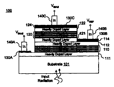
FIG. 1 shows one embodiment of a sensing pixel 100
of a dual-band array. A plurality of such pixels form
either a one-dimensional array or a two-dimensional
array. The pixel 100 includes two quantum-well
structures 110 and 120 that are stacked with each other
over a semiconductor substrate 101 and are configured to
respectively detect radiation of two different
wavelengths. The first quantum-well stack 110 has a
first number, N1, of quantum wells. The stack 110 absorbs
radiation at a first wavelength hl while transmitting
radiation at other wavelengths.
The second quantum-well stack 120 has a second
number, NZ, of quantum wells. The stack 120 absorbs
radiation at a second wavelength 1~2 while transmitting
radiation at other wavelengths. Hence, each quantum-well
stack transmits the non-absorbed radiation, rather than
blocking. The transmitted radiation by one stack is
detectable by another stack.
The two quantum-well stacks 110 and 120 may be
formed of the same semiconductor compounds with different
molar ratios of a particular element. For example,
AlGaAs (barrier)/GaAs(active layer) can be used to form
both stacks 110 abd 120 but the molar ratios of aluminum
are different so that the absorption wavelengths are
different. In addition, the quantum-well stacks 110 and
120 may be formed of different semiconductor compounds,
particularly, when the first and second wavelengths are
significantly different from each other. For example,
the first stack 110 may use AlxGa1_xAs/GaAs and the second
stack 120 may use All_xGa,_xAs/InyGal_~,As/GaAs or other
material combinations such as GaxInl_xP/InP. Other
CA 02306212 2000-04-14
WO 99/19912 PGTNS98/218i2
- 8 -
material combinations include, GaAs, InP, AIXInI_xP/InP and
In,sAl1_xAs /AlAs .
Each quantum-well stack is sandwiched between two
heavily doped semiconductor contact layers that are
electrically conductive (e. g., n ~ 10" c~i3~. A proper
bias voltage is applied to the quantum-well stack via the
contact layers. Dopant types of both contact layers are
the same. Hence, if a contact layer on one side of the
quantum-well stack is doped to have the n-type
conductivity, the contact layer on the other side of the
quantum-well stack should also have the n-type
conductivity. More specifically, the first quantum-well
stack 110 is formed between the contact layers 111 and
112 and the second quantum-well stack 120 is formed
between the contract layers 121 and 122. The contact
layers 121 and 112 are in contact to each other.
Alternatively, as illustrated in the pixel 200 shown in
FIG. 2, the adjacent contact layer 121 can be eliminated
so that a single contract layer 112 is shared by the
quantum-well stacks 110 and 120.
The material composition of a contact layer in
general can be any suitable semiconductor material.
Preferably, a contact layer may be selected according to
the material composition of the respective quantum-well
for lattice matching and easy fabrication. For example,
if AlGaAs is used to form a quantum-well stack, a
respective contact layer may be formed of heavily doped
GaAs and the substrate may be formed of undoped GaAs
which is semi-insulating.
The sensing pixel 100 receives input radiation
from the side of the first quantum-well stack 110. The
input radiation received by either quantum-well stack
(110 or 120) must have an electric field component along
CA 02306212 2000-04-14
WO 99/19912 PCT/US98JZ1812
_ g _
the growth direction of the quantum-well layers which is
perpendicular to the quantum-well layers in order to
induce an intersubband transition at a desired infrared
wavelength. See, Gunapala and Bandara, supra. For a
single IR detector or a linear array, the substrate 101
may be lapped at an angle (e. g., 45°) to effect a proper
coupling by directing the radiation perpendicular to the
angled facet. Such a coupling configuration, however,
cannot be used in a two-dimension sensing array.
One way to couple radiation at an angle to the
quantum-well layers uses reflective gratings at each
pixel (e. g., 100 or 200) to reflect normally incident
radiation rays inside pixel 100 to produce reflective
radiation rays having an electric field component along
the growth direction of the quantum-well layers.
Referring to FIG. 1, the second quantum-well stack
120 is preferably smaller than the first quantum-well
stack 100 to expose a portion of the contact layer 112
and to accommodate an electrode 1408. Two reflective
grating layers 114 and 124 are respectively formed over
the heavily doped contact layers 112 and 122 to provide
proper optical coupling to the quantum-well sensing
stacks 110 and 120. Such grating layers may be formed by
using photolithographic techniques to fabricate desired
grating features. The first reflective grating layer 114
may be configured to have grating features that reflect
the radiation of the first wavelength 1~1 at one or more
desired angles. The second reflective grating layer 124
may be fabricated to include two sets of reflective
grating features, one set for reflecting radiation of the
first wavelength A1 and another set for reflecting
radiation of the second wavelength J~2.
CA 02306212 2000-04-14
WO 99!19912 PCTIUS98/21812
- 10 -
In operation, input radiation is received from the
side of the sensing array that has the substrate 101.
Incident rays in the input radiation that are
substantially perpendicular to the array will not be
absorbed by either of the quantum-well stacks 110 and
120. However, such rays will be reflected by the
gratings 114 and 124 and re-enter the quantum-well stacks
110 and 120 from the opposite side at some angles and
will be absorbed.
Electrical bias to each quantum-well sensing stack
is provided through ohmic contacts. An ohmic contact
1308 (e. g., a metallic layer) is formed on the first
reflective grating layer 114 over the exposed portion of
the contact layer 112. The electrode 1408, e.g., an
indium bump, is formed over the ohmic contact 1308 to
supply a reference voltage VREF to the contact layers 112
and 121. Electrodes 140A, 140C are respectively formed
on ohmic contacts 130A, 130C on the contact layers 111,
122 for providing a common bias voltage VHI~ to both
quantum-well stacks 110 and 120. The electrodes 140A and
140C are shortened so that the voltage across each of the
quantum-well stacks 110 and 120 is (VBI~-VREF)
A readout multiplexer with an array of readout
capacitors for sensing the radiation-induced charge is
coupled to the two-band array to supply a single bias
voltage (VBI~) to and to read out the signals from, both
quantum-well stacks 110 and 120.in each pixel 100 or 200.
Such readout multiplexer may be implemented by a .
commercial readout multiplexer used in a single-band
quantum-well IR sensing array. This is well known in the
art. One implementation designates one readout pixel in
a readout multiplexer to one sensing pixel to read out
the two signals from both stacks 110 and 120. The two
CA 02306212 2000-04-14
WO 99/19912 PGT/US98/21812
- 11 -
signals from each sensing pixel may be read out
sequentially: reading the stack 110 first and then
reading the stack 120 after the capacitor is reset. Such
operation can increase the frame readout time.
It is often desirable, however, to simultaneously
measure the images of a target object at the two
different wavelengths A1 and 1~2 in many applications.
This may be done by simultaneously reading out the
radiation-induced charged carriers from the stacks 110
and 120 in each pixel. One way to obviate this problem
is to designate two readout pixels in the multiplexer
array to one sensing pixel where one readout pixel
corresponds to one sensing stack in the designated
sensing pixel. Therefore, the two stacks 110 and 120 can
l5 be simultaneously read out by the two corresponding
readout pixels in the multiplexer. Hence, for a sensing
array of M pixels, a respective readout multiplexer
should have 2M readout pixels. For example, two rows of
the readout pixels in the multiplexer are designated to
readout one row of the sensing pixels.
Each of the quantum-well stacks 110 and 120 is
configured to operate based on a special "bound-to-quasi-
bound" intraband transition (i.e., intersubband
transition) to increase the responsivity and the signal-
to-noise ratio. An absorption subband is described which
occurs when the first excited state is in resonance with
an area near the top of the barrier. Such transitions
exist when the thermionic emission energy barrier of the
quantum well (ET) is substantially matched to the energy
required for photoionization (EP), i.e., preferably within
2~ of precise resonance.
CA 02306212 2000-04-14
WO 99/19912 PCTNS98/21812
- 12 -
This bound-to-quasi-bound configuration has a
thermionic emission energy barrier which is increased
relative to the bound-to-continuum transitions. More
thermal energy is required to liberate an electron
confined in the quantum well. Dark current generated by
the quantum well during operation is therefore reduced.
However, since the excited state in the bound-to-
quasibound configuration is resonant with the thermionic
emission energy barrier, electrons can escape with little
or no tunneling. The quantum wells with this
configuration hence maintain a high quantum efficiency,
i.e., a large amount of photocurrent is generated by the
incident infrared photons. These two factors, low dark
current and high quantum efficiency, increase the signal-
to-noise ratio of the photocurrent generated by the
quantum well.
The bound-to-quasibound energy-level configuration
of the quantum wells in the stacks 110 and 120 is
obtained by controlling the properties and quantities of
the GaAs and AlxGa1_,sAs materials to effect the necessary
resonance relationship. The mole fraction of Al can be
increased to increase the well depth. The thickness of
the GaAs well layer can be decreased to increase the
separation between the ground and excited state and the
well depth. The preferred bound-to-quasibound
configuration results when the photoionization (EP) is
substantially equal to the thermionic emission energy
barrier. Under this condition, the excited state lies
below the continuum states and above the deep confined
quantum well states to form a quasi-bound state.
Since the excited state is near the barrier
potential, electrons in the excited state can be easily
pushed from this quasibound state into the continuum. An
CA 02306212 2000-04-14
WO 99/19912 PCT/US98/21812
- 13 -
important advantage. is that the photoexcited electrons
can escape from the quantum well to the continuum
transport states with little or no tunneling. This
allows reduction of the bias required to efficiently
collect the photoelectrons and hence reduces the dark
current. Moreover, since the photoelectrons do not have
to tunnel through thick barriers, the AlxGa1_xAs barrier
thickness of the bound-to-continuum quantume-well devices
can be increased without correspondingly reducing
photoelectron collection efficiencies. This embodiment
uses a barrier width is preferably 500 to 600 and the
quantum well width which is preferably 40 to 70~. This
is an increase of five over many conventional quantum-
well IR detectors. See, the incorporated Application
No. 08/785,350.
Assume the first quantum-well stack 110 is
configured as a MWIR detector and the second quantum-well
stack 120 is configured as a LWIR detector in the pixel
100 or 200. The energy-band diagram of the pixel without
an external bias can be illustrated in FIG. 3. Each
quantum-well stack is configured so that the excited
state in at or near the top the quantum well potential.
A bias voltage is applied across a quantum-well stack
preferably in a direction substantially perpendicular to
the quantum-well layers to shift the radiation-induced
charge in the excited state out of the quantum~wells.
FIG. 4 shows the energy-band diagram of a quantum-
well stack under a bias voltage across the quantum wells.
The energy barrier between two adjacent quantum wells is
slanted so that the radiation-induced charge in the
excited state in one quantum well, under the force caused
by the bias electric field, transports over the energy
barrier to the adjacent quantum well with a lower
CA 02306212 2000-04-14
WO 99/19912 PCT/US98/21812
- 14 -
electrical potential. Hence, this perpendicular bias
voltage induces a large photocurrent in parallel to the
bias electric field due to the large difference in the
carrier mobility between the ground and excited states.
In general, increasing the bias electric field can
enhance the transport process of the radiation-induced
charge, thereby increasing the output photocurrent.
However, the bias electric field cannot be too
large since the dark current also increases with the bias
electric field. The dark current is one primary source
of noise in quantum-well IR detectors. when the nias
electric field is greater than a certain value, the
contribution from the dark current may become significant
compared to the radiation-induced photocurrent so that
the signal-to-noise ratio of the output photocurrent is
degraded below a predetermined acceptable level.
Therefore, the bias electric field should be properly
selected to substantially optimize the responsivity while
still maintaining the signal-to-noise ratio above the
acceptable level.
Since the two quantum-well stacks 110 and 120 are
configured to respond to radiation at two different
wavelengths, the energy gaps between the ground and
excited states in the two stacks are different. The
quantum-well stack 110 for detecting radiation at a
wavelength in the MWIR range has a larger energy
separation between the respective ground and excited
states in the same band than the quantum-well stack 120
for the LWIR range. Hence, a larger bias electric field
is desired in the quantum-well stack 110 than that in the
stack 120 in order to cause a significant transport of
the radiation-induced carriers in both stacks and to
respectively optimize the responsivities.
CA 02306212 2000-04-14
WO 99119912 PCTNS98I21812
- 15 -
One feature of the pixel 100 or 200 is that the
numbers of the quantum wells, the widths of each well, or
both of the quantum-well stack 110 can be configured
differently from those parameters of the stack 120 so
that the same. bias voltage can be applied to both stacks
to achieve different bias electric fields within the
stacks to substantially optimize their responsivities.
The responsivity, R, of a quantum-well stack can
be approximately expressed in terms of the net quantum
efficiency, n, of the stack and the photoconductive gain,
g:
R = ( h~ ) n g.
where a is the electronic charge and by is the
photoexcitation energy. When the quantum efficiency of
each well n~, is low (nW « 1), the net quantum efficiency
r~ and the photoconductive gain g are approximately given
by:
r1 = rt~.Vr I2)
9 ~ NPc. L3)
where N is the number of quantum wells in the stack and p~
is the capture probability of each well. Hence, the
responsivity R of the stack is
CA 02306212 2000-04-14
wo ~nmz rcrnrsmam
- 16 -
R ~ ( by ) Pp . (4)
Hence, the responsivity R of a stack is approximately
independent of the number of the wells, N. The
dependence of the responsivity R on the bias electric
field across each well is primarily caused by the
variation of p~ with the bias electric field. The capture
probability p~ decreases as the bias electric field
increases and vice versa.
Assume the desired bias electric fields for the
stacks 110 and 120 are EH1 and EBZ, respectively. The
relation between the common bias voltage difference (Vg
Vo) and the optimized bias electric fields EB1 and EB2 is
Ve-Vo - EeiNiLPi - EazN2Lpa~
where N1 and N2, LPl and Lp2 are the numbers of quantum
wells, and the well widths of the stacks 110 and 120,
respectively. Therefore, as long as the number of the
wells, N, and the well width, Lp, of a quantum well are
configured to maintain the parameter, ENLp, as a constant
(i.e., the common voltage difference between each stack),
the bias electric fields and therefore the responsivities
of the two quantum-well stacks are set at the desired
values. When the two quantum-well stacks 110 and 120
have the same well width, the ratio of the numbers of
wells of the stacks 110 and 120 is selected to satisfy
the following:
CA 02306212 2000-04-14
WO 99/19912 PCT/US9$/21812
- 17 -
_Ni = Eaz . ( 6 )
Na Eai
Since EB1 > EB2, the number of wells N1 in the stack 110 is
less than the number of wells N2 in the stack 120.
The dark current noise associated with the dark
current Ip of a quantum-well stack can be approximately
expressed as
9el~f (7)
in = 4eglD~f = Np ,
c
where ~f is the frequency bandwidth. For a common number
of wells, the value of Ip/p~ for a LWIR detector is
usually a few orders greater than that of the a SWIR or
MWIR detector, the dark current noise of a dual-band
pixel 100 or 200 is dominated by the LWIR detector. When
the number of wells in the LWIR detector increases and
the number of the wells in the SWIR or MWiR detector
decreases, the dark current noise in the LWIR detector
decreases while the dark current noise in the SWIR or
MWIR detector increases. However, for many practical
devices, the dark current noise of the LWIR detector
still dominates when the quantum-well stacks 110 and 120
are configured according to Equation (5) or (6). Hence,
the dark current noise of the dual-band pixel 100 or 200
with N1 < N2 under a single bias voltage can be reduced
compared to the dark current noise of a dual-band pixel
with N1 = NZ under two bias voltages.
The doping density of the quantum wells, no, of
the each quantum-well stack (110 or 120) is another
CA 02306212 2000-04-14
wo 99n W z PCT/US98/21812
- 18 -
design parameter that can be varied to optimize the
performance of the sensing array. The doping density no
directly relates to the single well quantum efficiency
Therefore, the responsivity R in equation (4) is directly
proportional to no. The doping densities of the two
quantum-well stacks 110 and 120 can be set at different
values so that their respective responsivities are
different from each other.
For example, in certain applications, the amount
of IR radiation at the first operating wavelength 1~, of
the first stack 110 is different from the amount of IR
radiation at the second operating wavelength AZ of the
second stack 120 in an received image. It therefore may
be necessary to make the responsivity of the stack that
receives the weaker radiation higher than the other stack
by a higher doping density so that the received image
represented by the weaker radiation can be enhanced.
Specifically, assuming that two different fluxes
at different wavelengths received in the two different
sensing stacks are fl and f2, the photocurrents
respectively generated by the stacks 110 and 120, i1 and
i2, can be written as:
i1 = f 1 X Ri.
12 - f2 X R2i
where R1 and RZ are responsivities of the stacks 110 and
120, respectively and are defined in Eq.(4). If the
current i1 and i2 are significantly different from each
other, e.g., the difference is greater than one order of
magnitude, due to the difference in fl and f2, the readout
multiplexer array may not properly detect the current
signals i, and i2. For some readout multiplexers, it is
desirable to have the values of i, and iz on the same
order of magnitude. This can be achieved by adjusting
CA 02306212 2000-04-14
WO 99/19912 PCT/US98IZ1812
- 19 -
the quantum efficiency of each well nw, which is directly
related to the number of carriers, i.e., well doping
density, in the well. Hence, this well doping density
can be used as another design parameter to adjust the
quantum efficiency of each well and to optimize the
sensing array according to specific requirements of an
application. Other parameters, including, the number of
wells and the quantum well period, may also be adjusted
to change the electric field in each well. The electric
field in each well changes the capture probability pc.
Therefore, the doping density, number of wells and
quantum well period of the quantum-well sensing stacks
110 and 120 can all be adjusted in a relation with one
another so that the two sensing stacks produce
photocurrents of similar magnitudes in response to
radiation of different fluxes at two different
wavelengths.
In general, the number of quantum wells N, the
quantum well width Lp, and the doping density no can be
adjusted either independently or in combination to
provide design flexibility and to meet the performance
requirements of various applications.
FIG. 5 shows that a dual-band quantum-well sensing
array 510 having pixels shown in either FIG. 1 or in
FIG. 2 is engaged to a readout multiplexes array 520.
The indium pumps (e.g., 140A through 140C in FIG. 1) in
each pixel are connected to the respective pixel in the
readout multiplexes array 520.
The substrate 101 shown in FTGS. 1 and 2 may be
eliminated by, e.g., etching, to achieve certain
performance advantages. FIG. 6 shows one embodiment of a
dual-band quantum-well sensing pixel without a substrate.
The support for the sensing pixels is provided by the
CA 02306212 2000-04-14
WO 99/19912 PCT/US98J21812
- 20 -
readout multiplexes array 520. Since the multiplexes
array 520 is in general formed of a silicon substrate
which is different from the substrate 101 (e. g., GaAs),
the thermal expansion coefficients of the multiplexes
array 520 and the sensing array 510 with the substrate
101 are different. Different thermal contractions occur
when the device is cooled down to a low temperature and
may cause cracking.
Although dual-band quantum-well IR sensing arrays
are described, three or more quantum-well IR detectors at
different wavelengths may be implemented each pixel to
form a multi-band quantum-well IR sensing array. Also,
in an alternate embodiment, each reflective grating layer
(119 and 124) may be replaced by a special reflecting
layer which has surface roughness or small features
(either random or periodic) on the scale of the
wavelength. Normally incident radiation, upon reflection
by such a reflecting layer, is scattered back to the
sensing stacks 110 and 120 in a range of directions
(e.g., forming a cone) and is no longer perpendicular to
the quantum-well layers. Various other modifications and
enhancements may also be made, which are intended to be
encompassed by the appended claims.