Note: Descriptions are shown in the official language in which they were submitted.
CA 02307985 2000-OS-10
J p i~~ -~ ~' ~.~ '~.yr D
;, :~ i
TITLE OF THE INVENTION
Optical Recording Medi~,un
BACKGROUND OF THE INVENTION
Field of the Invention
This invention relates to an optical recording medium in which a light
transmitting layer of a thin thickness is bonded to a recording layer on a
substrate and
in which Light is irradiated from the side of the light transmitting layer to
record and/or
reproduce the information.
Description of Related Art
In an optical disc, such as the-called compact disc (CD), light is irradiated
from
the side of a transparent substrate, 1.2 ruin in thickness, to read out the
signals. The
transparent substrate is formed of a transparent thermoplastic resin and has
pits
formed on its surface. That is, the optical disc includes a light transmitting
layer, 1.2
mm in thickness, with pits being formed on its bottom surface.
In such case, the reproducing spot diameter cp of the playback light
irradiated
is represented by the following formula:
cp = 1.22 x a,/N
where ~. is the playback light wavelength and NA is the numerical aperture of
a lens.
With the playback light wavelength of 780 nm and the numerical aperture of a
lens NA of 0.45, for example, the playback light spot diameter is
approximately 2.1
,um. Since the spot diameter on the surface of the light transmitting layer
1.2 ruin in
CA 02307985 2000-OS-10
thickness is approximately 715 ,um, the playback light is not obstructed,
while errors
produced can be corrected, in a majority of cases, even if the dust affixture
or grazing
has occurred on the surface of the light transmitting layer.
There is also proposed, as an optical recording medium that is able to realize
recording to an outstandingly higher density than with the CD, such an optical
recording medimn having a light transmitting layer in the form of a sheet 3 to
177 ~cm
in thickness and which is adapted to irradiate the light from the side of this
sheet-like
light transmitting layer.
In this optical recording medium, in which the light transmitting layer is
extremely thin in comparison with the conventional transparent substrate,
obstruction
of the recording and/or reproducing light by dust deposition, or grazing
produced by
collision against the optical pickup or by sandwiching the affixed dust
between an
optical pickup and the light transmitting layer, presents serious problems.
If, with the recording and/or reproducing wavelength ~, = 515 nm, the
numerical
aperture of an objective lens of an optical pickup NA = 0.85 and the
refractive index
of the light transmitting layer n = 1.58, the playback spot diameter and the
spot
diameter on the surface of the light transmitting layer are estimated for the
light
transmitting layer with a thickness of 100 Vim, the playback spot diameter is
approximately 0.74 ,um, whereas the spot diameter on the surface of the light
transmitting layer is approximately 130 ,um. Since the spot area on the
surface of the
light transmitting layer is approximately 1/30 of that with the CD, and
approaches to
2
CA 02307985 2000-OS-10
the size of the dust and dirt encountered in our everyday life, sufficient
attention must
be paid to_deposition of dust and dirt or scratches with this sort of the
optical recording
medium.
It has hitherto been recognized that a transparent substrate formed of
polycarbonate tends to be grazed on collision with an optical pickup. In an
optical
recording medimn in which light is irradiated from the side of the light
transmitting
layer of reduced thickness, an optical pickup with a NA as high as 0.85 is
used, and the
distance between the light transmitting layer and the optical pickup (working
distance)
is set to not larger than 300 ~,cm, the grazing due to collision or to
sandwiching of dust
and dirt between the optical pickup and the light transmitting layer tends to
occur more
significantly than with the conventional .optical recording medium. Therefore,
if a
tetrafluoroethylene based material is used as a housing material for an
optical pickup,
and collision is produced at 20 Hz at a linear velocity of 5 m/sec, tracking
servo is in
trouble on occurrence of approximately 100 collisions to render error
correction during
readout impossible. In actuality, concentric grazing was observed to have
occurred on
the surface of the polycarbonate sheet.
SUMMARY OF THE INVENTION
It is therefore an object of the present invention to provide an optical
recording
medium in which the light transmitting layer may be prohibited from being
grazed or
deformed to cause no hindrance in recording and/or reproduction.
It is another object of the present invention to provide an optical recording
3
CA 02307985 2000-OS-10
medium which is superior in production efficiency and in mass-producibility.
The present inventors have conducted various researches, and found that, by
surface-processing the light transmitting layer at the outset with a view to
increasing
surface hardness, reducing the frictional coefficient and to preventing the
electrification, it is possible to realize recording and/or reproduction
within the range
of error correction despite the occurrence of collision of the optical
recording medium
against the optical pickup. The present inventors have also found that, by
measuring
the surface hardness of the light transmitting layer by the micro-Vickers
hardness
method or by the nano-indentation method, it is possible to quantitate the
hardness that
is able to stand the collision against the optical pickup.
The present invention has been completed based on, this information and
provides a support having a thickness of 0.3 mm to 1.2 mm, a recording layer
provided
on the support and a light transmitting layer provided on the recording layer
3 ~m to
177 ,um in thickness. The information is recorded and/or reproduced by the
light being
irradiated from the side of the light transmitting layer having a surface-
processed
surface.
Preferably, the light transmitting layer has a hardness not less than 13 HMV
in
terms of the Vickers hardness and a hardness not less than 0.5 GPa as measured
by the
nano-indentation method or a Young's modulus not less than 4 GPa as measured.
by
the nano-indentation method.
By the surface-processing, the surface of the light transmitting layer is
4
CA 02307985 2000-OS-10
prohibited from being damaged or deformed to assure recording and/or
reproduction
of high reliability.
That is, according to the present invention the light transmitting layer is
not
damaged or deformed even on collision of the optical pickup against the light
transmitting layer to assure recording and/or reproduction within the range of
error
correction.
Moreover, according to the present invention, since a surface-processed sheet
is used, the disc surface processing step after disc fabrication, which is to
be
performed from one completed disc to another, can be omitted, thus improving
production efficiency.
BRIEF DESCRIPTION OF THE DRAWINGS
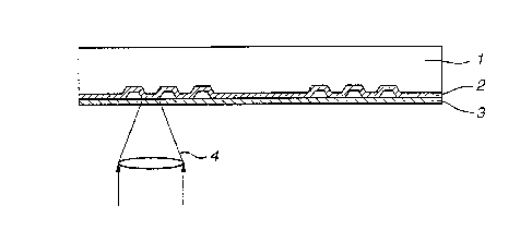
Fig. l is a schematic cross-sectional view showing an illustrative structure
of an
optical disc embodying the present invention.
Fig.2 is a schematic view showing an overall structure of a measurement device
used in the measurement by the nano-indentation method.
Fig.3 is a graph showing the load-displacement curve as measured by the nano-
indentation method.
DESCRIPTION OF THE PREFERRED EMBODIMENTS
Referring to the drawings, an optical recording medium according to the
present
invention will be. explained in detail.
Fig. l shows an example of an optical recording mediium embodying the present
CA 02307985 2000-OS-10
invention. In the optical recording medium, a recording layer 2 is formed on a
supporting substrate 1 and a light transmitting layer 3 is bonded thereon to
overlie the
recording layer 2. The information is written or read out from the side of the
light
transmitting layer 3 so that the optical pickup 4 is arranged facing the light
transmitting
layer 3.
As the recording layer 2, any suitable recording layer known to be usable as
the
recording layer of the optical recording medium may be used. For example, at
least
one of a reflective film, a phase-change recording filin, a photomagnetic
recording
film and an organic dye recording fihn, is formed as the recording layer 2.
The supporting substrate 1 is a molded article of e.g., thermoplastic resin,
and
has fine phase pits or guide grooves formed on its surface, on which the
recording .
layer 2 is formed as appropriate.
The light transmitting layer 3 is a thin polycarbonate sheet and has its
thickness
set to 3 to177 ,um at least in its recording area. By reducing the thickness
of the light
transmitting layer 3, a high NA optical pickup can be used to enable high
density
recording.
It is a characteristic of the present invention to use a sheet surface-
processed at
the outset as the sheet of the light transmitting layer 3 in order to realize
at least one
of the increase in surface hardness, reduction in the fi-ictional coefficient
and
prevention of electrification.
The surface hardness may be increased by using, as the sheet of the light
6
CA 02307985 2000-OS-10
transmitting layer 3, a sheet on which at least one of Si oxide, Si nitride,
Si carbide,
mixture of Si oxide and Si nitride, and hard carbon is fonned previously, or a
sheet
the on surface of which a liquid light curable resin or a liquid
thennohardening resin
has been coated and cured.
Preferably, the surface hardness of the light transmitting layer 3 has a
Vickers
hardness not less than 13 HMV, a hardness as measured by the nano-indentation
method of not less than 0.5 GPa or a Young's modulus not less than 4 GPa.
With the micro-Vickers hardness testing method, a diamond presser (micro-
Vickers presser) is pressed into the surface of a sample to measure the
hardness of the
sample. Using a diamond presser in the form of a tetragonal pyramid, with a
diagonal
surface of 136°, in teens of a thrusting hardness, a pyramid-shaped
indentation is
formed in the test surface. The load at this time is divided by the surface
area as found
from the mean length of the diagonal lines of the indentation. The destruction
tenacity
can be found by measuring the length of a crack produced at this time, while
the
toughness affording mechanism can be known by observing the interaction
between
the crack and the fine texture.
The present method has a feature that a small test piece suffices in
conducting
the test in measuring the hardness or tenacity.
It is however difficult to realize accurate measurement of the hardness of an
inorganic film-like material, with a thickness not larger than 1 ,um, obtained
on filin-
fonning by vapor deposition or sputtering. The reason therefor is that the
underlying
7
CA 02307985 2000-OS-10
layer operates as an influencing factor, and that, when the presser is forced
into the
bulk of the sample material, the thin film is cracked to render it impossible
to effect
accurate measurement of the diagonal line of the indentation.
On the other hand, the nano-indentation method is a method whereby the load
and the displacement during the defonnation process can be measured accurately
as
a small-sized diamond presser is forced into the bulk of the thin film. This
method is
being used for measuring the hardness or the modulus of elasticity of the thin
film or
investigating into the destruction behavior. It is noted however that the
sample
measurement is to be conducted at room temperature because the sample is
contacted
with the presser.
Fig.2 shows a typical measurement device by the nano-indentation method. This
measurement device includes an electro-magnet 6, mounted on the proximal end
of a
diamond presser 5, and which is supported by a spring 7. At back of the
diamond
presser 5 is arranged a magnet 8. The load of the diamond presser 5 on the
sample 9
is detennined by the interaction between the magnet 8 and the electro-magnet 6
for
load.
i
At a mid portion of the diamond presser 5 is mounted a capacitance
displacement meter 10 adapted for measuring the displacement of the diamond
presser
5.
In the above measurement device, load addition is by exploiting the electro-
magnetic induction or the piezoelectric effect. The load value is determined
by reading
s
CA 02307985 2000-OS-10
out the current value and by the load cell in the former and latter cases,
respectively.
The load used for experimentation is usually of an mN order, with the
resolution being
approximately 1 ,um. The displacement is determined with the resolution of
approximately 0.2 mN by measuring changes in capacitance.
Fig.3 shows a graph showing a typical load-displacement curve, as obtained by
the nano-indentation method. Since the deformation behavior accompanying the
forcing of the presser is complex, it is not possible to analyze the obtained
curve in its
entirety. However, it is possible to derive the modulus of elasticity and
hardness from
data in the vicinity of the maximum load (Pmax).
Assuming that the deformation at the initial stage of unloading is the elastic
deformation, the elastic constant Ee~. is related to the gradient S of a
tangent drawn to
the curve at the maximum load Pme,~ by
S- 2 . .~.~,e~,.
Oh the other hand, the hardness is derived from the well-known following
relationship:
H - Pm~,,~/A
where
(3 is the dimensionless factor dependent on the presser shape;
A is the contact area of the presser; and
9
CA 02307985 2000-OS-10
Een is the elastic constant.
It is noted that, in the case of a Berkovich presser, [3 and A are given by
the
following equation:
~i = 1.034
where
A = 24.5 h~2 and
h~ = hma,~ - 0.75 ~Pm~~JS.
On the other hand, the Young's modulus Ef of the thin film may be derived from
the measured value of the elastic constant E~ff by the following equation:
l~eff = ~ 1 - Vf ~Ef + ~ 1 - Vindenter2~~indenter
which takes the presser deformation into account. In the above equation,
V~,dznt~ _
0.07 and E;nd~,« = 1141 GPa.
It should be noted that, in the nano-indentation method, attention should be
paid
in the experimentation to the fact that, should the presser be forced to an
excessive
depth, the interface or the substrate operates as an influencing factor. The
results of
an experiment on an Al thin film on an Si substrate and calculations employing
an
infinite element method indicate that, if the presser depth is not larger than
1/10 to 1/5
of the film thickness, the effect of the substrate can be overlooked. This
value is used
as a measure in other thin films.
According. to the present invention, it is possible to use a sheet surface-
processed at the outset as the light transmitting layer 3 with a view not only
to
to
CA 02307985 2000-OS-10
increasing the surface hardness but also to reduction of the frictional
coefficient and
to preventing the electrification. For the fonner purpose, surface processing
is carried
out by coating e.g., silicone oil at the outset, whereas, for the latter
purpose, surface
processing is carried out by coating at least one of cationic surfactant and
the
amphoteric surfactant.
Examples
The present invention will now be explained with reference to specified
Examples.
ExamnlP~
A polycarbonate sheet, 100 yn thick, coated at the outset with a liquid
photocurable resin, to a thickness of 2 ,um, was punched to a disc shape, and
bonded
to an optical disc supporting substrate, 1.2 mm thick, using a liquid
photocurable resin,
as an adhesive, to fabricate a high density optical disc.
This liquid photocurable resin had a Vickers hardness of 40 HMV, which was
improved to approximately thrice that on the surface of a non-processed
polycarbonate
substrate. '
As a result, the risk of the light transmitting layer being damaged could be
lowered even if contamination of higher hardness such as sand or dust is
affixed to the
disc surface and sandwiched between the optical pickup and the light
transmitting
layer.
~xamnle 2
11
CA 02307985 2000-OS-10
A polycarbonate sheet, 100 ~cm thick, on which SiO~ ( 1 sx~2) was fonned to a
thickness .of 80 nm by sputtering, was punched to a disc shape, and bonded to
an
optical disc supporting substrate, 1.2 mm thick, using a liquid photocurable
resin, as
an adhesive, to fabricate a high density optical disc.
The surface hardness and the Young's modulus, as measured using a nano-
indentation method, as a thin film hardness measurement method, by a namo-
indicator
II, a trade name of a product manufactured by NAMO-INSTRUMENTS INC., were
approximately 2 GPa and approximately 17 GPa, respectively. Since the surface
hardness and the Young's modulus of an unprocessed polycarbonate sheet were
approximately 0.3 GPa and approximately 4 GPa, respectively, it may be seen
that the
high-density optical disc is desirably improved in surface hardness.
Moreover, the dynamic frictional coefficient on the disc surface can desirably
be reduced from 0.25 to 0.15 as a result of formation of an SiOx film.
The dynamic frictional coefficient was measured using HEIDON 22, a trade
name of a measurement device manufactured by SHINTO KAGAKU SHA CO. LTD.
under the measurement condition of a load of 20~gf and a measurement speed of
60
mm/min, using a stainless steel (SUS) ball 10 mm in diameter.
As a result ofthe reduction in the frictional coefficient, the nwnber of
scratches
on the optical disc medium, produced on contact of the optical pickup with the
light
transmitting layer, could be diminished.
Example 3
12
CA 02307985 2000-OS-10
A polycarbonate sheet, 100 ~.m thick, on which Si3N,, was fonned to a
thickness
of 150 nm by sputtering, was punched to a disc shape, and bonded to an optical
disc
supporting substrate, 1.2 rnln thick, using a liquid photocurable resin, as an
adhesive,
to fabricate a high density optical disc.
The surface hardness and the Young's modulus, as measured using a nano-
indentation method, as a thin filin hardness measurement method, by a NANO-
INDICATOR II, a trade name of a product manufactured by NANO-INSTRUMENTS
INC., were approximately 4 GPa and approximately 28 GPa, respectively. Since
the
surface hardness and the Young's modulus of an unprocessed polycarbonate sheet
were approximately 0.3 GPa and approximately 4 GPa, respectively, it may be
seen
that the high-density optical disc is desirably improved in surface hardness.
Moreover, the dynamic frictional coefficient on the disc surface can desirably
be reduced from 0.25 to 0.18 as a result of formation of an SiO,~ (lsxs2)
film.
The dynamic frictional coefficient was measured using HEIDON 22, a trade
name of a measurement device manufactured by SHINTO KAGAKU SHA CO. LTD.
under the measurement condition of a load of 20agf and a measurement speed of
60
mm/min, using a stainless steel (SUS) ball 10 mm in diameter.
As a result of the reduction in the frictional coefficient, the number of
scratches
on the optical disc medium, produced on contact of the optical pickup with the
light
transmitting layer, could be diminished. Even when the optical pickup was
caused to
impinge on the disc 1000 times at a line velocity of 5m/sec and 20 Hz, the
readout
13
CA 02307985 2000-OS-10
error frequency in the area was not increased, in marked distinction from the
optical
disc employing an unprocessed polycarbonate sheet, susceptible to an increased
error
correction frequency, as a light transmitting layer. By forming an Si3N~, film
on the
polycarbonate sheet, there was no problem caused in readout even on collision
of the
disc with the optical pickup.
m le 4
A cationic surface modifier IN-177B, manufactured by TAI~AMATSU YUSHI
CO. LTD., was applied on a polycarbonate sheet, 100 ~m in thickness, dried
with hot
air at 100 ° C and heat-treated at 120 ° C for three minutes to
coat the surface modifier
to a thickness of 1 ,um on the polycarbonate sheet.
The polycarbonate sheet, onwhich the cationic surface modifierwas pre-coated
to a thickness of 1 ,um, was punched to a disc shape, and bonded to an optical
disc
supporting substrate, 1.2 mm thick, using a liquid photocurable resin, as an
adhesive,
to fabricate a high density optical disc.
As a result, the surface resistance value was lowered from 1015 SZ/cm2 to 10'
S2cm2, as measured under the measurement conditions of 20 ° C and '~0
RH%, this
indicating that the amount of adhesion on the light transmitting layer by
static charges
could be diminished.
Example 5
A polycarbonate sheet, 100 ,um in thickness, was punched to a disc shape, and
bonded to an optical disc supporting substrate, 1.2 mm in thickness, using a
liquid
14
CA 02307985 2000-OS-10
photocurable resin as an adhesive. On this polycarbonate sheet was top-coated
silicone
oil manufactured by SHIN-ETSU KAGAKU KOGYO SHA C0. LTD. under the trade
name of KF-96, by a stamp system, to fabricate a high density optical disc.
As a result, the optical disc was improved in surface lubricity, with the
dynamic
fi-ictional coefficient now being decreased from 0.26 to 0.08. The dynamic
frictional
coefficient was measured by HEIDON 22 manufactured by SHINTO KAGAKU SHA
CO. LTD. using a 10 mm stainless steel (SUS) ball under a load of 20 gf and a
measurement speed of 60 mm/min.
In this manner, surface loss or deterioration of the light transmitting layer
on its
collision against an optical pickup could be reduced.
i