Note: Descriptions are shown in the official language in which they were submitted.
CA 02308621 2000-04-25
WO 00/14972 PCTIKR99/00508
AFC DEVICE AND METHOD OF CONTROLLING RECEPTION
FREQUENCY IN A DUAL-MODE TERMINAL
BACKGROUND OF THE INVENTION
i
1. Field of the Invention
The present invention relates generally to a device and method for
controlling the reception frequencies in a terminal in a mobile communication
system, and in particular, to a AFC (Automatic Frequency Control) device and
I e) method of a dual-mode terminal.
2. Description of the Related Art
Data is generally transmitted by a terminal in a mobile communication
system in an FDD (Frequency Division Duplexer) scheme or a TDD (Time
15 Division Duplexer) scheme. The next-generation mobile communication system
considers implementing a dual-mode terminal with the advantages of the two
schemes. Since the dual-mode terminal uses different frequency bands, it
requires
oscillators for generating the different frequencies and thus the design of an
AFC
(Automatic Frequency Controller) for the oscillators is increasingly
important. It
20 is difficult to apply different feed-back loops to the two oscillators in a
conventional terminal during a synchronization acquisition of different
frequencies.
FIG. 1 is a block diagram of an AFC circuit in a receiver of a dual-mode
terminal. Referring to FIG. I, a mixer 111 mixes an input signal RX with an
25 oscillation frequency received from a first voltage-controlled oscillator
(VCO1)
I 19 and outputs a first mixed signal Fc 1. A low-pass filter (LPF) 113 low-
pass
filters the output of the mixer 111. The output of the LPF 113 is the
amplitude A1
of the input signal. An analog-to-digital (AID) converter 11 S converts the
output
of the LPF 113 to digital data q_a bits. A mixer 131 mixes the input signal RX
3~ with an oscillation frequency received from a second voltage-controlled
oscillator
( VC02) 139 and outputs a second mixed signal Fc2. A LPF 133 low-pass filters
the signal received from the mixer 13I. The output of the LPF 133 is the
amplitude A2 of the input signal. An A/D converter 135 converts the output of
the
LPF 133 to a digital data cLb bit.
CA 02308621 2000-04-25
WO 00/14972 PCT/KR99/00508
-2-
.4n AFC I51 receives the digital data from the A/D converters 115 and
1 ss and generates a signal (RX main clock) for automatically controlling a
reception frequency. A TCXO (Temperature Compensated Crystal Oscillator) 153
s multiplies the output of the AFC 151 to generate an intended RF (Radio
hrcquency)/IF (Intermediate Frequency). A PLL (Phase Locked Loop) 117
~~enerates a control signal for generating a phase-locked frequency according
to the
multiplied signal received from the TCXO 153. The oscillator 119 generates the
ti-equency set under the control of the PLL 1 I7 and applies the frequency to
the
1 () mixer 1 I 1. A PLL 137 generates a control signal for generating a phase-
locked
Frequency according to the multiplied signal received from the TCXO 153. The
oscillator I39 generates the frequency set under the control of the PLL 137
and
applies the frequency to the mixer 131. A BBA circuit 155 generates a sampling
clock for the A/D converter ! 15 in response to the output of the TCXO 153. A
IS BBA (Base Band Analog) circuit 157 generates a sampling clock for the A/D
converter 135 in response to the output of the TCXO 153.
The oscillators generate different frequencies through the PLLs in the
receiving AFC circuit of the dual-mode terminal as constructed above.
Application of the above conventional AFC circuit to a dual-mode
transmission scheme has the following problems. The dual-mode terminal has
different RFs/IFs and employs the AFC circuit to stabilize each oscillator
when a
mode transitions to a different frequency band. Here, the AFC circuit operates
to
?5 acquire a frequency offset. To do so, it operates a feed-back loop within
the range
of the amount of residual frequency fitter enough to ensure the demodulation
performance at the receiving end, to thereby achieve stable performance.
However,
it takes a long time to establish a stabilized path by operating the feed-back
loop at
a mode transition, resulting in the increase of time required to ensure the
demodulation performance. As shown in FIG. 1, in the case that different
IFs/RFs
should be multiplied by one TCXO and controlled by different PLLs, a different
control dynamic range is set for each loop. Therefore, the amount of fitter in
the
phase noise error of each VCO output is different when controlling two
different
VCOs, thereby decreasing the demodulation performance of the receiver.
3$
CA 02308621 2000-04-25
WO 00/14972 PCTIKR99/00508
-3-
FIG. 2 is a graph illustrating the unequal dynamic range characteristics of
the receiving AFC circuit in the dual-mode terminal. Referring to FIG. 2,
reference numerals 222 and 224 denote two frequency slopes F1 step/V_step and
F?-stepiV_step of the TCXO 1 S3. Reference numerals 226 and 228 denote the
~(vnamic ranges of the first and second mixed signals Fcl and Fe2,
respectively.
Reference numeral 230 denotes the phase-noise margin of the frequencies output
from the TCXO 1 S3. As shown in FIG. 2, due to use of the TCXO 1 S3 in the AFC
circuit of the conventional dual-mode terminal, the AFC 1 S 1 has different
control
voltage to frequency transform dynamic ranges. Hence, a TCXO exhibiting
I 0 different slopes, as shown in FIG. 2, is required but difficult to design.
As described above, the receiving AFC circuit of the conventional dual-
mode terminal has the problem that either a different operation should be
executed
at each mode or the frequency error tracking time is extended by use of a
single
I S .AFC circuit. Another problem is that in the case of using one TCXO having
a
reference frequency for controlling two RFs/IFs, the dynamic ranges of the
phase
noise output with respect to the outputs of the two VCOs are different because
of
the residual phase noise of the TCXO, thereby decreasing the demodulation
performance of the receiving end.
SUMMARY OF THE INVENTION
It is, therefore, an object of the present invention to provide an automatic
frequency control circuit and a method thereof in a dual-mode terminal, which
can
2S stabilize frequency characteristics to increase demodulation performance.
It is another object of the present invention to provide an automatic
frequency control circuit and a method thereof in a dual-mode terminal, which
can
vary the quantization level of digitized data to improve linear frequency
transform
characteristics.
It is a further object of the present invention to provide an automatic
frequency control circuit and a method thereof in a dual-mode terminal, which
l ntroduces a forward common phase error compensation scheme to increase
3S demodulation performance.
CA 02308621 2000-04-25
WO 00/14972 PCTIKR99/00508
-4-
To achieve the above objects, there is provided an AFC circuit in a dual-
mode terminal. According to one aspect of the present invention, the AFC
circuit
includes a first IF generator having a first frequency oscillator, for
generating a
First IF by mixing a first input signal with a first oscillation frequency. In
the AFC
circuit. a frst AID converter receives a first quantization step value,
allocates
c~uantization bits to obtain a first linear characteristic, and then converts
the first IF
to digital data. A second IF generator has a second frequency oscillator, and
generates a second IF by mixing a second input signal with a second
oscillation
ti~equency. A second AID converter receives a second quantization step value,
allocates quantization bits to obtain a second linear characteristic, and then
converts the second IF to digital data. An automatic frequency controller
(AFC)
receives the first and second digital data and automatically controls the
frequency
of a main clock based on the linear characteristics of the two input signals.
A
I S multiplier multiplies the clock and applies the multiplied clock to the
first and
second frequency oscillators.
According to another aspect of the present invention, the AFC circuit
includes a first IF generator having a first frequency oscillator, for
generating a
tirst IF by mixing a first input signal with a first oscillation frequency. A
first A/D
converter converts the first IF to digital data, a second IF generator has a
second
frequency oscillator, for generating a second IF by mixing a second input
signal
with a second oscillation frequency, and a second AID converter converts the
second IF to digital data. An AFC receives the first and second digital data
and
?5 automatically controls the frequency of the main clock based on the linear
characteristics of the two input signals. A first frequency monitor monitors
the
frequency of the first input signal. A multiplier receives a clock and the
outputs of
the first frequency monitor and the AFC, multiplies the clock, and applies the
multiplied clock to the first and second frequency oscillators. A PDS monitor
3Q receives the first IF and PDS information of the multiplier, and generates
a PDS
monitoring signal. A phase error estimator estimates the phase error from the
outputs of the second AID converter and the PDS monitor, and a multiplier
multiplies the phase error by the output of the second AID converter to
thereby
co»-ecr the phase error.
CA 02308621 2002-09-19
75998-83
4a
According to another aspect of the present
invention, there is provided an automatic frequency
controlling method in a dual-mode terminal, comprising the
steps of: generating first and second Intermediate
Frequencies (IFs) by mixing first and second input signals
with first and second oscillation frequencies; determining a
quantization gain and a transform rate according to the
linear characteristics of the first and second IFs and
generating first and second digital data; automatically
controlling the frequencies of the first and second digital
data and generating a clock signal; and generating the first
and second IFs according to the clock signal.
According to a further aspect of the present
invention, there is provided an automatic frequency
controlling method in a dual-mode terminal, comprising the
steps of: generating first and second Intermediate
Frequencies (IFs) by mixing first and second input signals
with first and second oscillation frequencies; generating
first and second digital data according to the linear
characteristics of the first and second IFs; monitoring the
tracking error component of the first input signal while
estimating a phase error, loading the estimated frequency
error value as an initial value to be used in generating a
clock signal, and generating the clock signal; and
generating the first and second oscillation frequencies
according to the clock signal, estimating a phase error when
an automatic control loop for the second input signal starts
tracking, and compensating for the phase error.
CA 02308621 2000-04-25
WO 00/14972 PCT/KR99/00508
-5-
BRIEF DESCRIPTION OF THE DRAWINGS
The above and other objects, features and advantages of the present
invention will become more apparent from the following detailed description
when
taken in conjunction with the accompanying drawings in which:
F1G. 1 is a block diagram of an AFC circuit in a dual-mode terminal
according to the prior art;
FIG. 2 is a graph illustrating the unequal dynamic range in the AFC circuit
of the dual-mode terminal shown in FIG. 1;
I () FIG. 3 is a block diagram of a dual-mode AFC circuit using an adaptive
Ai D quantization bit assigning method according to an embodiment of the
present
invention;
FIGS. 4A and 4B are block diagrams of the AFC circuit for bit assignment
in the dual-mode terminal shown in FIG. 3; and
15 FIG. 5 is a block diagram of a dual-mode AFC circuit with a forward
common error compensating function according to another embodiment of the
present invention.
DETAILED DESCRIPTION OF THE PREFERRED EMBODIMENTS
Preferred embodiments of the present invention will be described
hcreinbelow with reference to the accompanying drawings. In the following
description, well-known functions or constructions are not described in detail
since
they would obscure the invention in unnecessary detail.
The following description is conducted with the appreciation that first and
second input signals indicate RX1 and RX2, respectively, first and second IFs
indicate Fcl and Fc2, respectively, and first and second quantization steps
indicate
F l step/V step and F2 step/V step, respectively.
In a dual-mode terminal using an AFC circuit and a TCXO which can
support a dual mode, the AFC circuit and the TCXO generate errors due to
different linear characteristics. Therefore, the dual-mode terminal reduces
the IF
errors caused by the different linear characteristics in two modes by reducing
time
required for acquiring tracking synchronization of a PLL circuit in a mode
using a
CA 02308621 2000-04-25
WO 00114972 PCT/KR99/00508
-6-
first frequency by use of a test augmentation frequency which is an integer
multiple of a tracking synchronization acquiring residual frequency of a PLL
circuit for a second frequency to which the first frequency transitions for
reliable
synchronization acquisition, so that demodulation performance is ensured.
Other<vise. errors with respect to a dynamic range, caused by the different
linear
characteristics at a mode transition, are reduced by varying the quantization
bits of
the A/D clock signal based on the dynamic range of residual errors in
frequency, to
thereby ensure the demodulation performance.
I () The demodulation performance can also be ensured by operating an ACPE
(Advanced Common Phase Error) circuit for an AFC circuit having many residual
frequency errors. In this method, the frequency characteristics of the dual-
mode
terminal are stabilized and the stability of a demodulator is increased due to
a
frequency offset. As a result, the stable demodulator performance is ensured.
IS
There are three methods of overcoming the problems with use of a single
TC'XO with respect to a signal having two different RF frequencies in the AFC
circuit of the above dual-mode terminal: (1) using a TCXO which can support
both
modes; (2) appropriately selecting a quantization level to obtain two linear
20 characteristics; and (3) compensating for residual phase errors in one
linear
characteristic with respect to the other linear characteristic, in a forward
direction
in the baseband. That is, the TCXO satisfies a linear characteristic at one
mode,
and a linear characteristic at the other mode is satisfied by compensating for
residual phase errors of digitized data. The above three methods of ensuring
the
25 stable characteristics of an AFC circuit can be applied to a dual-mode
terminal
according to the costs involved in configuring the receiving terminal.
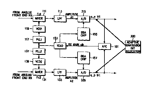
Referring to FIGS. 3, 4A, and 4B, there will be given a description of the
operation of an AFC circuit in a dual-mode terminal according to an embodiment
30 of the present invention. FIG. 3 is a block diagram of the AFC circuit
which
improves linear frequency characteristics using an adaptive AID quantization
bit
assigning method. FIGs. 4A and 4B are block diagrams of the A/D converters 315
and 335, respectively.
35 Referring to FIG. 3, the mixer 111 mixes the input signal RX with an
CA 02308621 2000-04-25
WO 00/14972 PCT/KR99100508
_7_
oscillation frequency received from the oscillator 119 and outputs the first
mixed
signal Fc 1. The LPF 113 low-pass filters the output of the mixer 111. The
output
of the LPF I I3 is an amplitude A1 of the input signal. The AID converter 315
convents the output of the LPF 113 to digital data q-a bit. The AID converter
315
pan be configured as shown in FIG. 4A. Referring to FIG. 4A, a maximum
amplitude detector 412 detects a maximum amplitude MAX A1 of the amplitude
.~ 1 of the input signal RX received from the LPF 113. A quantization gain
controller 416 generates a control signal for controlling quantization gain in
response to a first quantization step F1 step/V_step. A quantization bit
allocator
-l l4 generates quantization level information according to the maximum
amplitude
MAX-.-~1 and the quantization gain control signal received from the
quantization
~~ain controller 416. An AID converter 410 receives the first quantization
level
information and converts the input signal with the amplitude A to digital data
cLa.
I ~ The mixer 131 mixes the input signal RX with an oscillation frequency
received from the oscillator 139 and outputs the second mixed signal Fe2. The
L.PF I s 3 low-pass filters the signal received from the mixer 131. The output
of the
LPF Is3 is an amplitude A2 of the input signal. The AID converter 135 converts
the output of the LPF 133 to digital data q-b bit.
The AID converter 335 can be configured as shown in FIG. 4B. Referring
to F1G. 4B, a maximum amplitude detector 422 detects a maximum amplitude
iblAX_A2 of the amplitude A2 of the input signal RX received from the LPF 133.
A quantization gain controller 426 generates a control signal for controlling
quantization gain in response to a second quantization step F2 step/V step. A
quantization bit allocator 424 generates second quantization level information
according to the maximum amplitude MAX-A2 and the quantization gain control
signal received from the quantization gain controller 426. An AID converter
420
receives the second quantization level information and converts the input
signal
3(> with the amplitude Awis to digital data q_b bit.
The AFC 151 receives the digital data q_a bit and eLb bit from the AID
converters 115 and 135 and generates a signal (RX main clock) for
automatically
controlling a reception frequency. The TCXO 153 multiplies the output of the
z ~ A FC 1 ~ 1 to generate an intended RFIIF. The PLL 1 117 generates a
control signal
CA 02308621 2000-04-25
WO 00/14972 PCT/KR99/OOS08
_g_
for generating a phase-locked frequency according to the multiplied signal
received from the TCXO 153. The oscillator VCO1 119 generates the frequency
set under the control of the PLL1 117 and applies the frequency to the mixer
111.
The PLL2 137 generates a control signal for generating a phase-locked
frequency
,according to the multiplied signal received from the TCXO 153. The oscillator
VC'02 139 generates the frequency set under the control of the PLL2 137 and
applies the frequency to the mixer 131. The BBA circuit 155 generates a
sampling
clock for the A/D converter 115 in response to the output of the TCXO 153. The
BBA circuit 157 generates a sampling clock for the AID converter 135 in
response
I () to the output of the TCXO 153.
(n order to control the quantization level for the A/D conversion, the slope
of a phase detector for the AFC 1 S 1 is determined by an input quantization
level.
That is, input levels of the phase detector should be designed to be different
to
I 5 represent two linear characteristics. The levels of the input signals Fcl
and Fe2 in
FIG. 3 should be set to have different linear characteristics so that the AFC
151 can
operate with stability. To determine the input levels, the AFC 151 calculates
a
quantization gain value for AID conversion by
2 r,
20 IC,~_-..........(1)
2A
where b represents the quantization level for the AID conversion and A is the
maximum amplitude of the received signal.
25 Since the quantization level is the slope of the phase detector for the AFC
151, the level slopes of inputs of the TCXO 153 can be controlled by varying
quantization bits. The quantization level determines a phase compensation
resolution, and as the phase compensation resolution decreases, the
sensitivity to
phase errors increases.
A quantization conversion rate should be considered in determining the
quantization level because a noise margin component should be taken into
account
in AID conversion. The quantization rate is the ratio of the quantization
level of
the A/D converter 315 to that of the AID conveter. The quantization conversion
CA 02308621 2000-04-25
WO 00/14972 PCT/KR99/00508
-9-
rate is given by
_ 2'' R
K - - * - ..........(2)
'' 2 A ( 00
In Eq.2, quantization data qad a bit and qad b bit are generated by
determining a quantization level so that the slope of the quantization gain
shows
the two linear characteristics of the TCXO 153. [IS R THE CONVERSION
RATE?]
1 () Therefore, the AID converters 315 and 335 determine the input levels of
the received signal having different linear characteristics. The A/D
converters 315
and 335 determine quantization bits so that the slope of quantization gain
shows
the two linear characteristics of the TCXO 153, and they convert input signals
to
digital data. Then, the AFC I 51 receives the data q_a bit and q-b bit from
the AID
I S converters 115 and 135 and rapidly performs phase synchronization. That
is, by
appropriately selecting the quantization bits in such a way to obtain the two
linear
characteristics, the AFC 151 can rapidly acquire phase synchronization. The
TCXO 153 multiplies the RX main clock received from the AFC 151 and applies
the multiplied RX main clock to the PLLs 117 and 137. Reference numeral 300
20 indicates that the AID converters 315 and 335 adaptively allocate
quantization bits
according to the linear characteristic of each mode.
Now, the operation of a dual-mode automatic frequency cantrai circuit
using an ACPE (Advanced Common Phase Error) will be described referring to
25 F1G. S.
The mixer 111 mixes the input signal RX with an oscillation frequency
received from the oscillator 119 and outputs the first mixed signal Fcl. The
LPF
I 13 low-pass filters the output of the mixer 111. The output of the LPF 113
is an
30 amplitude A 1 of the input signal. The A/D converter 115 converts the
output of
the LPF I 13 to digital data q_a bit.
The mixer 131 mixes the input signal RX with an oscillation frequency
received from the oscillator 139 and outputs the second mixed signal Fc2. The
CA 02308621 2000-04-25
WO 00/14972 PCT/KR99/00508
- 10-
LPF 133 low-pass filters the signal received from the mixer 131. The output of
the
LPF 133 is an amplitude A2 of the input signal. The AID converter 135 converts
the output of the LPF 133 to digital data q_b bit.
s The AFC 151 receives the digital data q_a bit and cLb bit from the A/D
converters 11 S and 135 from the AID converters 115 and 135 and a choice
indicator from a terminal control (not shown), and generates a signal (RX main
clock) for automatically controlling a reception frequency. A first frequency
monitor 511 generates an initial loading frequency error from the output of
the
I () AFC 1 ~ 1. Specifically, the first frequency monitor 511 loads a
frequency error that
the AFC 151 has at the previous mode as an initial value and applies it to the
TCXO 153. The TCXO I53 multiplies the output of the AFC 151 and the initial
loading frequency error to generate an intended RF/IF. The PLL1 117 generates
a
control signal for generating a phase-locked frequency according to the
multiplied
l5 signal received from the TCXO 153. The oscillator VCOI 119 generates the
ti-equency set under the control of the PLL1 117 and applies the frequency to
the
mixer 111. The PLL2 137 generates a control signal for generating a phase-
locked
frequency according to the multiplied signal received from the TCXO 153. The
oscillator VC02 l 39 generates the frequency set under the control of the PLL2
137
20 and applies the frequency to the mixer 131. The BBA circuit 155 generates a
sampling clock for the AID converter 115 in response to the output of the TCXO
f s3. The BBA circuit 157 generates a sampling clock for the AID converter 135
in response to the output of the TCXO 153.
25 A PDS (Phase Density Spectrum) monitor 153 receives PDS information
from the TCXO 153 and the second mixed signal Fc2 from the mixer 131 and
monitors a PDS. A phase error estimator 1 S 1 measures the phase difference
between the PDS signal received from the PDS monitor S I3 and the data q_a bit
from the AID converter 135. A multiplier 517 multiplies the outputs of the A/D
30 converter 135 and the phase error estimator 515 and re-compensates the
digitized
data.
The dual-mode AFC circuit of FIG. 5 compensates for the noise margin of
FIG. 2 at the receiving end using the characteristics of the TCXO 153. To do
so,
35 the signal Fc 1 is first designed to have a small dynamic range, the PDS
monitor
CA 02308621 2000-04-25
WO 00/14972 PCTIKR99/00508
513 monitors the PDS characteristic of the TCXO 153, and the phase error
estimator 51 estimates a common phase error (CPE) by analyzing the PDS signal.
Simultaneously, the frst frequency monitor 511 monitors the tracking error
component of Fc 1 and loads the corresponding frequency error as the initial
loading frequency error when the loop of Fc2 operates. Then, when the Fc2 loop
atarts tracking, the phase error estimator 515 is operated to thereby obtain
the CPE
value and compensate for the phase error of the AFC 151 based on the CPE
value.
More specifically, the initial loading value is set to a stable frequency
I 0 transition value by the first frequency monitor 511 of Fc 1 and then the
CPE is
obtained.
To obtain the CPE, the PDS characteristic of the TCXO 153 is monitored,
an ekda value is determined, and then the PDS of a phase noise is obtained.
The
I 5 PDS is calculated by
10-°
L<nN (.r) = 10-~ + 10 !z-f' : f 1 < f ......(3)
f!+f~)
f~_ f, : f ~ fl
where fl and a are the PLL characteristics frequency and gain, respectively,
f2 is a
ti-equency with respect to the noise floor of a characteristic curve, b is the
slope of
the characteristic curve, and c is a noise floor value.
The above PDS characteristic remains as the residual frequency offset of
the phase detector, and a phase noise is obtained in the phase error estimator
515 of
FIG. 5 and is compensated for at the next end. The phase error is estimated by
Nr
~,~rt.~ ~e,.~,.~
o _ _ ;°~ ..... (4)
~lln.r
,-
where N,_ is an observation period, n~,., is an estimated amplitude value
obtained by
CA 02308621 2000-04-25
WO 00114972 PCT/KR99/08508
-12-
a channel estimation compensator, and 8,; ~i, i is the phase of the previous
symbol.
The influence of linear frequency characteristics on residual phase noise can
be
compensated for by re-compensating the CPE obtained in the above procedure at
the next end of the channel estimated value. Therefore, the AFC can be
stabilized.
In accordance with the present invention, when a dual-mode terminal uses
one or two AFC circuits, the time required for acquiring tracking
synchronization
in a PLL circuit for a first frequency can be reduced using a test
augmentation
frequency, which is an integer multiple of a tracking synchronization
acquiring
I () residual frequency of a PLL circuit for a second frequency to which the
first
frequency transitions for reliable synchronization acquisition. Errors with
respect
to the output dynamic range caused by use of two AFCs are reduced and thus the
demodulation performance of a receiver is ensured by varying the quantization
bits
of the A/D clock based on the dynamic range of residual errors in frequency.
The
I 5 demodulation performance can also be ensured by operating an ACPE circuit
for
an AFC circuit having many residual frequency errors. In this method, the
frequency characteristics of the dual-mode terminal are stabilized and the
stability
of a demodulator is increased due to a frequency offset. As a result, the
stable
demodulator performance is ensured.
While the invention has been shown and described with reference to a
certain preferred embodiment thereof, it will be understood by those skilled
in the
art that various changes in form and details may be made therein without
departing
from the spirit and scope of the invention as defined by the appended claims.