Note: Descriptions are shown in the official language in which they were submitted.
CA 02308684 2000-OS-17
BACKGROUND OF THE INVENTION
1. Field of the Invention
This invention relates to a diamond sintered compact excellent in economy
as well as cutting edge strength, in particular, a diamond sintered compact
tool whose diamond sintered compact layer thickness is decreased.
2. Description of the Prior Art
At the present time, diamond sintered compacts have been produced for
applying to industrial uses such as cutting tools, dies, bits, etc., and
used as a dresser, drill bit, wire drawing die, etc. for cutting or working
nonferrous metals, plastics, ceramics, etc. Among these tools, in particular,
a diamond sinterd compact tool used for a cutting tool is generally composed
of a tool material comprising a diamond sintered compact layer having a thick-
ness of about 1 mm to 1.5 mm and a WC-Co type cemented carbide substrate
banded
therewith during a step where diamond grains are sintered with each other, the
tool material being cut in a predetermined shape to give a cutting edge of a
tool and then brazed to a tool body.
The above described diamond sinterd compact tool has excellent proper-
ties for cutting of non-ferrous metals, etc. and has already widely been used.
However, since the diamond sintered compact has a higher tool unit cast be-
cause of its higher production or working cost as compared with other tool ma-
terials, it is indispensable to lower the tool unit cost in order to spread
more widely the diamond sintered compact tool. As a trial to lower the tool
unit cost, it is considered to decrease the cost for raw materials or finish-
ing a cutting edge by decreasing the thickness of the diamond sinterd compact
layer. However, a diamond sintered compact tool having a diamond layer thick-
ness of 0.8 mm to 1.5 mm has ordinarily been used in spite of that in
practical
uses of the diamond sintered compacts, there are often cases where a thickness
of at most 0.5 mm is sufficient. This is probably due to occurrence of a
problem that when the diamond layer is thinner, the strength of the diamond
sintered compact is decreased in spite of the material being a same diamond
CA 02308684 2000-OS-17
sintered compact and breakage resistance during working is inferior.
SUMMARY OF THE INVENTION
It is an object of the present invention to provide a material for a
high strength diamond sintered compact tool, whereby the above described prob-
lems of the prior art can be solved.
It is another object of the present invention to provide a diamond sin.-
tered compact tool having an excellent cutting edge strength and high break-
age resistance with a low production cost.
These objects can be attained by a diamond sintered compact cutting tool
comprising a diamond sintered compact sintered at an ultra-high pressure and
high temperature range such that diamond is present in stable manner and a WC-
Co
type cemented carbide substrate directly bonded to the diamond sintered
compact
during a step of sintering and. brazed to a tool body through the WC-Co type
cemented carbide substrate, in which a-ratio of the thickness of the WC-Co
type
cemented carbide substrate to the thickness of the diamond sintered compact
layer satisfies the relation of:
0.8 ~ WC-Co type cemented carbide substrate/diamond sintered
compact (Poly-Crystal 1 ine Diamond, PCD) layer ~ 3. 0
and the diamond sintered compact layer has a thickness of 0.05 mm to 0.45 mm,
preferably 0. 12 mm to 0. 36 mm.
BRIEF DESCRIPTION OF THE DRAWINGS
The accompanying drawings are to illustrate the principle and merits of
the present invention in more detail.
Fig. 1 is a perspective view of a sample model of a diamond sintered com-
pact cutting tool by a simulation graphic to illustrate a stress state thereof
in the case of a diamond sintered compact layer thickness of 0.8 mm and a WC-
Co
type cemented carbide substrate to diamond sintered compact layer thickness
ratio of 1.
Fig. 2 is a perspective view of a sample model of a diamond sintered com-
- 2 -
CA 02308684 2000-OS-17
pact cutting tool by a simulation graphic to illustrate a stress state thereof
in the case of a diamond sintered compact layer thickness of 0.5 mm and a WC-
Co
type cemented carbide substrate to diamond sintered compact layer thickness
ratio of 2.
Fig. 3 is a perspective view of a sample model of a diamond sintered com-
pact cutting tool by a simulation graphic to illustrate a stress state thereof
in the case of a diamond sintered compact layer thickness of 0.4 mm and a WC-
Co
type cemented carbide substrate to diamond sintered compact layer thickness
ratio of 3.
Fig. 4 is a perspective view of a sample model of a diamond sintered com-
pact cutting tool by a simulation graphic to illustrate a stress state thereof
in the case of a diamond sintered compact layer thickness of 0.3 mm and a WC-
Co
type cemented carbide substrate to diamond sintered compact layer thickness
ratio of 4.
Fig. 5 is a perspective view of a sample model of a diamond sintered com-
pact cutting tool by a simulation graphic to illustrate a stress state thereof
in the case of a diamond sintered compact layer thickness of 0.2 mm and a WC-
Co
type cemented carbide substrate to diamond sintered compact layer thickness
ratio of 7.
Fig. 6 (A) and (B) are enlarged photographs showing presence or absence
of chipping of diamond sintered compact cutting tools according to the present
invention and prior art after a cutting working test, depending on the WC-Co
type cemented carbide substrate to diamond sintered compact layer thickness
ratio, (A) being of a sample of the present invention and (B) being of that
for
comparison.
DETAILED DESCRIPTION OF THE INVENTION
The inventors have made various efforts to obtain a low-priced and high
fracture resistance diamond sintered compact for the purpose of achieving the
above described objects and consequently, have reached the present invention.
That is, the present invention can be accomplished by making clear an
- 3 -
CA 02308684 2000-OS-17
occasion of lowering of the breakage resistance by decreasing the thickness .
of a diamond sintered compact layer to smaller than the thickness (0.8 mm to
1.5 mm) of the commonly used diamond sintered compact tool and comprises the
specified constructions of the present invention summarized below:
(1) A diamond sintered compact cutting tool comprising a diamond sintered
compact sintered at an ultra-high pressure and high temperature and a WC-Co
type cemented carbide substrate directly bonded to the diamond sintered
compact
during a step of sintering and brazed to a tool body through the WC-Co type
cemented carbide substrate, in which a ratio of the thickness of the WC-Co
type
cemented carbide substrate to the thickness of the diamond sintered compact
layer satisfies the relation of:
0.8 < WC-Co type cemented carbide substrate/diamond sintered
compact layer < 3.0
and the diamond sintered compact layer has a thickness of 0.05 mm to 0.45 mm,
preferably 0. 12 mm to 0. 36 mm.
(2) The diamond sintered compact cutting tool, as described in the above
(1), wherein the diamond grains forming the said diamond sintered compact have
a grain size distribution of 0.5 a m to 30 a m, preferably I a m to 10 a m.
(3) The diamond sintered compact cutting tool, as described in the above
(1) or (2), wherein thermal stress applied to the surface of the cutting tool
edge during or after brazing the diamond sintered compact to the tool body
through the WC-Co type cemented carbide substrate is a compressive stress.
(4) The diamond sintered compact cutting tool, as described in any one
of the above (1) to (3), wherein the WC-Co type cemented carbide substrate
has a th i ckness of 0. I to 0. 9 mm.
(5) The diamond sintered compacvt cutting tool, as described in any one
of the above (1) to (4), wherein the brazing is carried out by the use of a
silver brazing material, preferably consisting of 30 to 70 weight % of Ag and
the balance of at least one of Cu, Zn and Ni.
(6) A diamond sintered compact material comprising a diamond sintered
- 4 -
CA 02308684 2000-OS-17
compact sintered at an ultra-high pressure and high temperature and a WC-Co
type cemented carbide substrate directly bonded to the diamond sintered
compact
during a step of sintering, in which a ratio of the thickness of the WC-Co
type
cemented carbide substrate to the thickness of the diamond sintered compact
layer satisfies the relation of:
0.8 ~ WC-Co type cemented carbide substrate/diamond sintered
compact layer <-_ 3.0
and the diamond sintered compact layer has a thickness of 0.05 mm to 0.45 mm,
preferably 0. 12 mm to 0. 36 mm.
PREFERRED EMBODIMENTS OF THE INVENTION
The fundamental principle of the above described inventions (1) to (6)
will now be illustrated hereinafter. Generally, a diamond sintered compact
and cemented carbide substrate have respectively a coefficient of thermal
expansion of 4. 0 x 10-6/K and (5 ~- 6) x 10 6/K. In a step of making
a finished tool from a diamond sintered compact material, the diamond sintered
compact material is exposed to a high temperature, e.g. at least 600 C during
discharge working or brazing to a tool body material. During the same time,
an internal stress occurs in the diamond sintered compact layer due to differ-
ence in coefficient of thermal expansion between the diamond sintered compact
layer and cemented carbide substrate and it is considered that when this
thermal stress is converted into a tensile stress at the cutting edge part,
the cutting edge strength is lowered to deteriorate the breakage resistance.
From the above described standpoint of view, it is found as a result of
our various studies that when the thickness of a diamond sintered compact
layer
and cemented carbide substrate is changed, the stress applied to the surface
of the tool edge is changed from tensile stress to compressive stress. Thus,
furthermore, we the inventors have studied such a condition that the stress
applied to the surface of the tool edge is converted into compressive stress,
and conseuQently, have found that the compressive stress appears when the
thickness ratio satsfies the relationship of:
- 5 -
CA 02308684 2000-OS-17
WC-Co type cemented carbide substrate/diamond sintered
compact layer < 3.0
The present invention is based on the thus obtained knowledge.
Therefore, as the thickness of a WC-Co type cemented carbide substrate is
thinner, the stress on a cutting edge surface area is a stronger compressive
stress and the breakage resistance of the cutting edge is more increased.
If the WC-Co type cemented carbide substrate is excessively made thinner,
however, a large tensile stress acts at the interface between the WC-Co type
cemented carbide substrate and diamond sintered compact layer to lower the
interfacial strength. Thus, the thickness ratio should suitably be:
0.8 S WC-Co type cemented carbide substrate/diamond sintered
compact layer < 3.0
Considering the balance of the stress on the cutting edge surface area
and that at the interfacial part between the WC-Co type cemented carbide sub-
strate and diamond sintered compact layer, it is confirmed more preferable to
adjust the thickness ratio to the Following:
l < WC-Co type cemented carbide substrate/diamond sintered
compact layer < 2
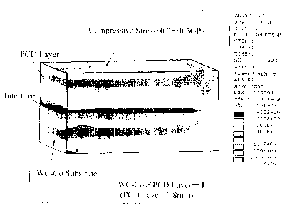
As shown in the accompanying drawings, Fig. 1 to Fig. 5 (computer graph-
ics attached herein), the thermal stress state acting on the surface of the
diamond sintered compact layer varies depending on the thickness ratio of
the WC-Co type cemented carbide substrate and diamond sintered compact layer,
in which a negative value indicates a compressive stress value and a positive
value indicates a tensile stress value.
It can readily be understood from these graphics that when cemented car-
bide thickness/diamond layer thickness ratio (WC-Co/PCD Layer Ratio) - 4 or 7,
the diamond sintered compact is subject to tensile stress through heating,
when the ratio = 3, the stress is substantially zero and when the ratio = 1 or
2, compressive stress acts thereon.
Thus, it can be assumed that the strength of the diamond sinterd compact
- 6 -
CA 02308684 2000-OS-17
layer is lowered, that is, the tool performance is deteriorated by the action
of the tensile stress on the surface of the diamond sintered compact layer.
Accordingly, it can be concluded from the simulation results that such a shape
or dimension is required as a tool shape that no or little tensile stress is
reactd during brazing heating and the relationship of:
WC-Co type cemented carbide substrate/diamond sintered
compact layer ~ 3.0
gives the most suitable structure.
The effectiveness of the above described computer simulation can clearly
be proved because of being in good agreement with the tendency of the tool
performance when subjected to real working as is evident from Examples, in
particular, Example 2.
Fig. 6 (A) and (B) are photographs respectivgely of a sample of the pre-
sent. invention and that for comparison, that is, diamond sintered compact
cutt-
ing tools, taken from their rake faces, to show presence or absence of
chipping
of the cutting edges after a cutting working test, depending on the WC-Co type
cemented carbide substrate to diamond sintered compact layer thickness ratio.
As can be seen from these photographs, in the case of the sample having
the WC-Co type cemented carbide substrate to diamond sintered compact layer
thickness ratio within the scope of the present invention, there is scarcely
found chipping, whilst in the case of the comparative sample having the thick-
ness ratio outside the scope of the present invention, a number of drippings
are found at the cutting edge.
On the other hand, the thinner is the thickness of the diamond sintered
compact layer, the more advantageous from the standpoint of production cost.
Since it is difficult to stably produce a diamond sintered compact having a
thickness of less than 0.05 mm, however, a thickness of at least 0.05 mm is
required.
In the present invention, as the diamond sintered compact and WC-Co type
cemented carbide substrate, there can be used commonly used, well-known
diamond
CA 02308684 2000-OS-17
sintered compacts and WC-Co type cemented carbide substrates. The WC-Co ce-
mented carbide used in the present invention includes not only those
comprising
to 25 weight % Co and the balance of WC as a predominant component, but also
those further containing some quantity of Ti, Ta, etc. As a shape of the
diamond sintered compact material, any type of ordinary inserts, cutting
tools,
dr i 1 1 s, reamers, etc. can be app 1 i ed.
In the present invention, the thickness of the diamond sintered compact
layer can be rendered thinner without deteriorating the breakage resistance of
the cutting tool edge, because a stress state on the surface of the cutting
tool edge is analyzed and a compressive stress state is obtained on the
surface
of the cutting tool edge, as illustrated above. That is, the stress state
in the diamond sintered compact can be well-balanced by adjusting the thick-
ness ratio of the diamond sintered compact layer and WC-Co type cemented
carbide
substrate to:
0.8 ~ WC-Co type cemented carbide substrate/diamond sintered
compact layer ~ 3.0
whereby the breakage resistance and the interfacial strength at the interface
between the WC-Co type cemented carbide substrate and diamond sintered compact
layer can be maintained. Accordingly, it is possible to provide a diamond
sintered compact tool having a sufficient breakage resistance with a low
price.
Moreover, the thickness of the diamond sintered compact layer is so thin,
for example, as represented by 0.05 mm to 0.45 mm that during cutting edge
finish-machining, an amount of scraped diamond is decreased to reduce the
machining cost.
In the present invention, furthermore, brazing can generally be carried
out at a temperature of 700 to 800 °C using a silver brazing material,
for
example, brazing material consisting of 30 to 70 weight % of Ag and the
balance
of Cu, Zn, 'Vi, etc. A number of other silver brazing materials are known and
can also be used in the present invention.
The present invention will now be illustrated in detail by the follow-
_ g
CA 02308684 2000-OS-17
ing Examples without limiting the same.
Example 1
A disk made of a cemented carbide (WC-6 % Co) with a diameter of 29.5 mm
and a thickness of 2 mm was arranged in a capsule made of Ta with an inner
diameter of 30 mm. On the cemented carbide disk were charged diamond grains
having a grain diameter of 0.5 to 4 a m, which was then covered further with a
Co plate with a diameter of 29.5 mm and thickness of 0.05 mm and a disk made
of
cemented carbide with a diameter of 29.5 mm and a thickness of 3 mm and
lightly
compressed at a pressure of about 100 MPa. The diamond grains were charged
in charged amounts as shown in Table 1.
When this capsule was processed at an ultra-high pressure and high tem-
perature, for example. a pressure of 5.5 GPa and a temperature of 1450
°C,
a diamond sintered compact with a thickness shown in Table l, sandwiched in
between the cemented carbide disks, was formed. In order to obtain a struc-
ture suitable for a tool material, the cemented carbide on one side of the
sintered compact was completely removed by means of a surface-grinding ma-
chine and electric discharge working device. Consequently, there was obtained
a material for a diamond sintered compact tool havi~~g a total thickness of
about 2 mm and comprising a structure of a diamond sintered compact layer
with a thickness of 0.2 to 0.25 mm bonded to a cemented carbide substrate.
Then, from the thus obtained diamond sintered compact material was scraped
off the base part of the cemented carbide as shown in Table 1.
This diamond sintered compact material was cut in a predetermined shape
and brazed to a tool body to prepare a tool for a milling cutter diamond
sintered compact brazed to one corner of cemented carbide. in the form of a
regular triangle with an inscribed circle of 9.525 mm, insert relief angle
Il°
(overall periphery) and thickness 3.18 mm, and a cutting edge in R-shape of
rod i us of 0. 4 mm} .
Using the resulting cutting tool, an estimation test of the cutting proper-
ties was carried out under the following conditions shown in Table 2, thus
g
CA 02308684 2000-OS-17
obtaining results shown in Table 3, in which brazing had been carried out
using JIS 23261 BAg-3 as a brazing material by heating in a high frequency
heat-
ing apparatus at about 750°C.
o-
CA 02308684 2000-OS-17
Table
Sample Charged Amount Thickness of Diamond Thickness of Cemented 2,/ i
No. of Diamond Sintered Compact Carbide Substrate 2:
(g) Layer 1 (mm) (mm)
1 1.0 0. 45 0.4 0. 89
2 1.0 0. 45 0.9 2. 0
3 0. 8 0. 36 0. 3 0. 83
4 0.8 0. 36 0.5 1. 39
0.6 0. 28 0.3 1. 07
6 0.6 0. 28 0.5 1. 79
7 0. 4 0. 18 0. 5 2. 7
8
8 0. 4 0. 18 0. 3 1. 6
7
9 0. 4 0. 18 0. 2 1. 11
0. 3 0. 14 0. 4 2. 8
6
1 1 0. 3 0. 14 0. 2 1. 4
3
12 0. 15 0. 0 7 0. 1 l 4
. 3
Comparison
13 0.6 0. 28 1.0 3. 57
14 0. 4 0. 18 0. 6 3. 3
3
Table 2
Workpiece: Round Rod of Al - 16 weight % Si alloy having six grooves
along axial direction
Cutting Rate: 500 m/min
Cutting Depth: 0.6 mm
Feed Rate. 0.12 mm/rev
Cutting Time. 3 minutes, wet process
- 1 1 -
CA 02308684 2000-OS-17
Table 3
Sample yo. Flank Wear Width
f a m)
26
2 32
3 24
4 28
27
6 30
7 31
8 29
9 26
32
11 28
12 31
Comparison
13 broken
14 broken
It will clearly be understood from Table 3 that the tool using the diamond
sintered compact material according to the present invention exhibits an ex-
cellent cutting edge strength without breakage of the cutting edge.
- 1 2 -
CA 02308684 2000-OS-17
Example 2
In an analogous manner to Example l, various materials each having a
thickness of a diamond sintered compact and a thickness of a cemented carbide
substrate were prepared as shown in Table 4. This diamond sintered compact
material was cut in a predetermined shape and brazed to a tool body made
of a cemented carbide to prepare a tool for a milling cutter. 100 test
pieces were prepared from these samples, after which cutting edge working
was carried out using a diamond wheel of grain size ~ 800 and NC tool grinding
disk to examine the yield rate depending on the thickness of the diamond sin-
tered compact layer. In Table 5 are shown the number of working tests, the
number of inferior goods and the contents of inferior goods, from which it is
apparent that the diamond sintered compacts according to the present invention
exhibit the feature that less breakages occur during cutting edge working and
the productivity is more excellent.
In comparison of Sample No. 16 according to the present invention and
Sample No. 19 according to the prior art, as can clearly be seen from Fig. 6
(A) and (B), a number of chippings are found in the case of Sample No. 19,
but chippings are scarcely found in the case of Sample No. 16 according to
the present invention.
- 1 3 -
CA 02308684 2000-OS-17
Table 4
Sample Thickness of DiamondThickness of Cemented 2 y
/
No. Sintered Compact Carbide Substrate 2
Layer 1 (mm) (mm)
15 0. 4 5 0. 9 2. 0
16 0. 28 0. 3 1. 07
l 7 0. 18 0. 3 1. 6
7
18 0. 0 7 0. 2 2. 8
6
Comparison
19 0. 7 0.7 1
20 0. 45 1. 8 4
21 0. 28 1. 0 3. 57
Table 5
Sample No. Number of Inferior Yield Rate (%) Contents of Inferior
Goods Occurred Goods Occurred
15 1 99 out of size spec.
16 0 100 NAB
17 1 99 chipping
18 2 98 chipping
Comparison
19 98 2 out of size spec.
20 44 56 chipping
21 33 67 chipping
note: not available
Advantages of Present Invention
The diamond sintered compact material according to the present invention
has an excellent strength when used as a tool material for a cutting tool,
excavator, etc.
- 1 4 -