Note: Descriptions are shown in the official language in which they were submitted.
CA 02308947 2000-05-19
Circuit arrangement for igniting a lamp
The present invention relates to a circuit arrangement
for igniting a lamp, in particular a high-pressure
discharge lamp, having an ignition transformer which
has a primary side and a secondary side, the secondary
side being connectable to the lamp which is to be
ignited, and the primary side being connected to an
ignition switch.
To illustrate the problem on which the invention is
based, Figure 1 shows such a circuit arrangement, as is
known from the prior art. A capacitor Cl is charged
from a DC voltage source UG via a resistor R1. The
capacitor C1 is then discharged, by shorting a spark
gap FS, via the primary side L1 of the ignition
transformer TR, until it is empty. As an alternative to
the spark gap, other self-triggering circuit breakers,
for example SIDACs, or triggerable circuit breakers,
for example thyristors or triacs, are also used in this
case. The large current flowing through the primary L1
of the ignition transformer TR is transferred to the
secondary L2 of the ignition transformer and causes the
lamp LA to be ignited there. The capacitor CL shown in
Figure 1 allows for the capacitance between the two
lamp wires, which is usually between 20 and 200 pF,
depending on the distance between the ignition circuit
and the lamp LA. The field in which such circuit
arrangements are used includes high-pressure discharge
lamps, which, in respect of their diverse applications,
can be regarded as a mass-produced product.
The object of the present invention is to refine a
circuit arrangement of the type mentioned in the
introduction such that production costs and complexity
CA 02308947 2000-05-19
- 2 -
are lower than for the circuit arrangement known from
the prior art.
To achieve this object, the present invention provides
that the ignition switch can be controlled for actively
disconnecting a current flowing through the primary
side of the ignition transformer.
The solution according to the invention is based on the
knowledge that, provided that the ignition switch can
be controlled for actively disconnecting a current
flowing through the primary side of the ignition
transformer, the store used for the ignition energy can
also be a charge store storing more charge than is
necessary for the ignition process. In a particularly
advantageous embodiment, to provide the ignition
energy, the primary side of the ignition transformer is
therefore connected to any desired DC voltage source,
which is provided anyway in the circuit, for example to
the intermediate circuit capacitor of the circuit
arrangement for operating the lamp. This solution
allows the components R1 and Cl shown in Figure 1 to be
dispensed with. As a result of the charging time
constant determined by R1 and Cl disappearing, the
invention provides the option of producing, in
principle, ignition pulses of the same amplitude which
follow one another at any desired rate.
The variable turned-on duration of the ignition switch
also permits the ignition pulse amplitude to be
influenced. This effect can advantageously be used to
compensate for component tolerances and, in particular,
the influence of the output capacitance in such a way
that the amplitude of the ignition voltage produced
remains virtually constant. The result of this is very
reliable lamp ignition.
CA 02308947 2000-05-19
- 3 -
In one advantageous implementation, the primary of the
ignition transformer is arranged between the
intermediate circuit capacitor and the ignition switch.
A component, particularly an inductor, which limits the
rise in current and is arranged in the current path on
the primary side and/or the secondary side of the
ignition transformer is used to prevent an undesirably
high current from flowing as soon as the ignition
switch has been turned on. This component acts in
addition to the leakage inductance of the ignition
transformer, which is always present anyway, but allows
other degrees of freedom when designing the ignition
transformer.
However, the solution according to the invention also
provides the basis for taking into account other
demands on an ignition circuit: considering the basic
circuit (shown in Figure 1) for a circuit arrangement
for igniting a lamp, this cannot, for many lamps, in
particular high-pressure discharge lamps, always
produce ignition pulses causing the lamps to be ignited
reliably, even if the individual circuit parameters are
optimized. The specification for an ignition pulse is
frequently defined in standards, for example in the
American standard ANSI M98, which defines the
electrical data for operating a "70W Single Ended HID
Lamp". For a load capacitance CL of 20 pF, the minimum
ignition pulse level should be 3 kV, the maximum
ignition pulse level should be 4 kV and the minimum
pulse width should be 1 s @ 2.7 kV. The minimum pulse
repetition rate should be 240 Hz.
Using circuit arrangements based on the basic circuit
shown in Figure 1, an ignition pulse satisfying these
ANSI M98 criteria could not be produced within the
framework of a sensible physical size for the ignition
transformer or without severely impairing the normal
CA 02308947 2000-05-19
- 4 -
operation of the lamp, that is to say operation after
ignition.
In this case, it should be taken into account that
contradictory conditions arise when designing the
ignition transformer, particularly the secondary side:
first, for normal operation, that is to say after
ignition of the lamp, L2 needs to be proportioned such
that the internal resistance is low, and, secondly, for
ignition, L2 needs to be proportioned such that it
allows a wide ignition pulse to be produced. Whereas
the first condition requires an L2 with few windings,
an L2 with a large number of windings is necessary for
the second condition. For these different demands, it
is not possible to find a satisfactory solution on the
basis of the basic circuit shown in Figure 1.
The situation is different with a particularly
advantageous embodiment of the invention: if provision
is made for a capacitor to act in parallel with the
secondary of the ignition transformer, the capacitor
and the secondary of the ignition transformer being
able to form a resonant circuit having a predetermined
resonant frequency and a predetermined maximum peak
voltage, then a sinusoidal ignition pulse can be
generated which can be used to satisfy the electrical
demands on the ignition pulse, particularly in terms of
its width. In this instance, L2 can have few windings,
for low resistance during operation of the lamp, that
is to say after ignition. The load capacitance
influences can also be drastically reduced as a result.
When implemented, the capacitor acting in parallel with
the secondary can be a capacitor connected in parallel
with the secondary of the ignition transformer, or a
capacitor connected in parallel with the connection
terminals of the lamp. The latter variant is suitable
if there is an output filter capacitor at the output of
the lamp current generator which is usually present.
CA 02308947 2000-05-19
- 5 -
Since the capacitance value of the output filter
capacitor is much higher than the capacitance value of
the capacitor connected in parallel with the connection
terminals of the lamp, a voltage change on the output
filter capacitor during pulse generation remains small.
The capacitor connected in parallel with the connection
terminals of the lamp thus acts as if it were arranged
in parallel with the secondary of the ignition
transformer. The advantage of this implementation
produces an additional filtering action on the current
in normal operation and consequently results in more
favorable RFI values. The ignition pulse remains
largely unaffected by the arrangement of the capacitor
acting in parallel with the secondary of the ignition
transformer.
Whereas the circuit arrangement shown in Figure 1 can
be used to produce only a cosinusoidal ignition pulse,
the particularly preferred embodiment of the present
invention can now be used to produce a sinusoidal
ignition pulse, which can be used to satisfy the
requirement regarding ignition pulse width, for example
1 s @ 2.7 kV in accordance with ANSI M98, see above,
much more easily.
So that the energy stored in the ignition circuit can
freewheel on the primary side when the ignition switch
has been turned off, the invention proposes that the
ignition switch be connected to the intermediate
circuit capacitor, on the one hand via the primary side
of the ignition transformer and on the other hand via a
clamp circuit. This is particularly advantageous to
prevent the ignition switch from being destroyed, for
example if the lamp is faulty and hence ignition does
not take place.
In a first embodiment, the clamp circuit comprises a
diode and a zener diode in reverse-connected series
with one another. They ensure that the voltage on the
CA 02308947 2008-11-24
, =
66498-109
6
ignition switch is limited and that the ignition transformer
is demagnetized until the next ignition pulse.
Alternatively, the clamp circuit can comprise a
diode arranged in series with a parallel circuit comprising
a capacitor and a nonreactive resistor. The advantage of
such a clamp circuit is that the pulse energy can be stored
in the capacitor "quickly" and can be reduced "slowly" by
the nonreactive resistor until the next ignition pulse.
However, another provision may be that, in place
of the aforementioned clamp circuits, the main electrode of
the ignition switch is connected to the DC voltage source,
preferably the intermediate circuit capacitor, on the one
hand via the primary side of the ignition transformer, and
on the other hand via a series circuit comprising a
capacitor and a first diode, and the reference electrode of
the ignition switch is connected to the junction point
between the capacitor and the first diode via the series
circuit comprising a second diode and an inductor. This
circuit measure is known from DE 298 02 174.9. It allows
complete feedback of the energy stored in the ignition
transformer, which allows very high ignition pulse
repetition rates to be produced with practically no losses.
In a modification of this circuit measure, a third diode is
arranged between the intermediate circuit capacitor and the
junction point between the inductor and the second diode.
In a particularly advantageous embodiment, the
ignition transformer has an iron-powder core. This allows a
very low secondary-side nonreactive resistance to be
achieved for the ignition transformer, which means that
losses during continuous operation of the circuit
CA 02308947 2008-11-24
66498-109
7
arrangement, that is to say after ignition, can be kept at a
low level. The iron-powder core also affords the advantage
that relatively high-frequency parasitic oscillation
components in the ignition pulse are greatly attenuated.
The result is that an almost ideally sinusoidal ignition
pulse without relatively high-frequency oscillation
components can be produced.
According to one aspect of the present invention,
there is provided a circuit arrangement for igniting a lamp
comprising: an ignition transformer having a primary side
and a secondary side, the secondary side being connectable
to the lamp which is to be ignited, and the primary side
being connected to an ignition switch, the ignition switch
actively disconnects current flowing through the primary
side of the ignition transformer, and wherein a component
that limits a rise in current is arranged in a current path
on one of a primary side and a secondary side of the
ignition transformer.
According to another aspect of the present
invention, there is provided a circuit arrangement for
igniting a lamp comprising: an ignition transformer having a
primary side and a secondary side, the secondary side being
connectable to the lamp which is to be ignited, and the
primary side being connected to an ignition switch, wherein
the ignition switch actively disconnects a current flowing
through the primary side of the ignition transformer; and a*
capacitor in parallel with the secondary side of the
ignition transformer, wherein the capacitor and the
secondary side of the ignition transformer form a resonant
circuit having one of a predetermined resonant frequency and
a predetermined peak voltage.
CA 02308947 2008-11-24
66498-109
7a
According to still another aspect of the present
invention, there is provided a circuit arrangement for
igniting a lamp comprising: an ignition transformer having a
primary side and a secondary side, the secondary side being
connectable to the lamp which is to be ignited, and the
primary side being connected to an ignition switch, wherein
the ignition switch actively disconnects current flowing
through the primary side of the ignition transformer; and a
capacitor in parallel with the secondary side of the
ignition transformer, wherein the capacitor is proportioned
such that an essentially sinusoidal ignition pulse is
produced.
According to yet another aspect of the present
invention, there is provided a circuit arrangement for
igniting the lamp comprising: an ignition transformer having
a primary side and a secondary side, the secondary side
being connectable to the lamp which is to be ignited, the
primary side being connected to an ignition switch, wherein
the ignition switch actively disconnects current flowing
through the primary side of the ignition transformer; and an
intermediate circuit capacitor connected to the primary side
of the ignition transformer, a first side of the ignition
switch being connected to the intermediate circuit capacitor
through the primary side of the ignition transformer, and a
second side of the ignition switch being connected to the
intermediate capacitor through a clamp circuit.
Other advantageous embodiments of the invention
can be found in the subclaims.
Illustrative embodiments of the invention are
described in more detail below with reference to the
appended drawings, in which:
CA 02308947 2008-11-24
66498-109
7b
Figure 1 shows a basic circuit, known from the
prior art, for igniting a lamp;
Figure 2 shows a schematic illustration of a basic
circuit diagram of a circuit arrangement in accordance with
a first embodiment of the present invention;
Figure 3 shows a schematic illustration of a basic
circuit diagram of a circuit arrangement in accordance with
a second embodiment of the present invention, and
Figure 4 shows a schematic illustration of a basic
circuit diagram of a circuit arrangement in accordance with
a third embodiment of the present invention.
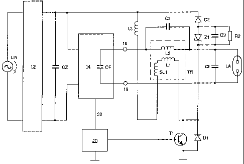
Figure 2 is a schematic illustration of a circuit
arrangement for igniting and operating a lamp LA, in
particular a high-pressure discharge lamp. The input of a
rectifier 12 is connected to a mains voltage source UN,
while its output is connected to an intermediate circuit
capacitor CZ. The intermediate circuit capacitor CZ
provides a DC voltage for the components
CA 02308947 2000-05-19
- 8 -
arranged to the right thereof in the circuit
arrangement. A lamp current generator 14 is arranged in
parallel with the intermediate circuit capacitor CZ,
and an output filter capacitor CF is connected in
parallel with the output terminals 16, 18 of said lamp
current generator 14. One end of the secondary L2 of an
ignition transformer TR is connected to the output
terminal 16. The lamp LA which is igniting is arranged
between the second end of the secondary L2 of the
ignition transformer TR and the output terminal 18 of
the lamp current generator. In parallel with the lamp
LA, a capacitor CL allows for the capacitance actually
originating from the lamp wires. A capacitor C2 is
arranged in parallel with the secondary L2 of the
ignition transformer TR. The series circuit comprising
the primary Ll and the primary-side leakage inductance
SL1 of the ignition transformer TR is connected, on the
one hand, to the intermediate circuit capacitor CZ via
an inductor L3, and, on the other hand, to the main
electrode of a switch T1. A freewheeling diode Dl is
reverse-connected in parallel between the main
electrode and the reference electrode of the switch Tl.
The control electrode of the switch Tl is connected to
an ignition controller 20, which, for its part, is
connected to the lamp current generator 14 via a line
22. The line 22 permits a signal to flow from the lamp
current generator 14 to the ignition controller 20, and
vice-versa. The reference electrode of the switch T1 is
connected to the intermediate circuit capacitor CZ by
means of a reverse-connected series arrangement
comprising a zener diode Z1 and a diode D2. An
alternative to the zener diode Zi is shown in dashes,
said alternative comprising a capacitor C3 and a
nonreactive resistor R2.
The circuit arrangement shown in Figure 2 operates as
follows for igniting the lamp LA:
CA 02308947 2000-05-19
- 9 -
On an enable pulse for the ignition controller 20 of
defined duration, which is applied to the control
electrode of the switch Ti, said switch turns on, also
for a defined duration, that is to say it permits a
current to flow in the main current's direction of flow
from the main electrode to the reference electrode over
a particular period of time. The switch T1 can, as an
example, be an IGBT power transistor capable of
interrupting even high ignition currents. Accordingly,
for the period for which the switch T1 is turned on, a
primary-side ignition current flows - driven by the
intermediate circuit capacitor CZ, which acts as a DC
voltage source - through the series circuit comprising
L3, SL1, L1 and T1 to ground. The inductor L3 interacts
with the leakage inductance SL1 and limits the rise in
the primary-side ignition current as soon as the switch
T1 has turned on. Without the capacitor C2, this would
nevertheless result in an almost cosinusoidal curve for
the ignition current through the secondary L2 of the
ignition transformer TR. However, since, as already
mentioned above, an ignition pulse which is as
sinusoidal as possible is desired for the ignition
pulse width, a capacitor C2 is connected in parallel
with the secondary L2 of the ignition transformer TR.
With suitable proportioning, this allows a resonant
circuit to be produced at a predetermined frequency and
with a predetermined peak voltage, and consequently a
sinusoidal, relatively wide ignition pulse.
So that the energy stored on the primary side can
freewheel, particularly if ignition has not taken place
on account of a faulty lamp LA, for example, a clamp
circuit comprising the diode D2 and the zener diode Z1
is provided. It is used to limit the voltage on the
switch T1 and to demagnetize the ignition transformer
until the next ignition pulse. As an alternative to
this, the clamp circuit can also be produced from the
diode D2 connected in series with the parallel circuit
comprising a capacitor C3 and a nonreactive resistor
CA 02308947 2000-05-19
- 10 -
R2. The capacitor C3 is used for quickly storing the
pulse energy, whereas the resistor R2 permits slow
reduction of the pulse energy until the next ignition
pulse.
The ignition transformer TR preferably has an iron-
powder core, for example an EF 32 iron-powder core from
HARTU, made of material No 629. The inductor L3 can be
a yarnreel core inductor from FASTRON, this inductor
having an unsaturated inductance of 100 H.
In the alternative embodiment shown in Figure 3, the
resonant circuit capacitor C2 is connected in parallel
with the lamp LA. In terms of the way it works when the
lamp LA is ignited, this has no negative influence
provided that the output filter capacitor CF is large,
because the voltage change on the output filter
capacitor CF then remains small during pulse
generation. In the embodiment shown in Figure 3, the
same reference symbols as in Figure 2 denote the same
components and are therefore not described again. The
embodiment shown in Figure 3 affords the advantage that
the secondary L2 of the ignition transformer TR and the
resonant circuit capacitor C2 form an RF filter stage
which further reduces RF components of the lamp current
which have an interfering effect on low-frequency lamp
operation. This also reduces the radiated interference
from the circuit arrangement.
In the circuit arrangement shown in Figure 4, in which
the same reference symbols as in Figure 2 denote the
same components, a circuit section comprising a diode
D2, a capacitor C4, an inductor L4, a diode D3 and a
diode D4 is provided instead of a clamp circuit, and
the branch having the diode D3 can be dispensed with,
if necessary. This expansion of the ignition circuit
allows complete feedback of the energy stored in the
ignition transformer, and the way it works is described
in detail in DE 298 02 174.9. It allows very high
--------------
CA 02308947 2000-05-19
- 11 -
ignition pulse repetition rates of up to several 10 kHz
to be achieved with virtually no losses. In this
arrangement, the resonant circuit capacitor C2 can also
be arranged in parallel with the connections of the
lamp LA, as in Figure 3, without restricting operation.
The circuit concept according to the invention can be
used to produce ignition pulses with an ignition pulse
width which is greater by a factor of 10 than that in
the circuit arrangement shown in Figure 1. When re-
igniting from hot, the lamps could be started again
even after an approximately 30% shorter cooling period.
The circuit concept according to the invention is also
distinguished by good reproducibility of the ignition
pulses.