Note: Descriptions are shown in the official language in which they were submitted.
CA 02310025 2000-02-14
WO 99/08825 1 PCT/DE98/02091
Assembling electroconductive harts b~,r electric current heating
The invention relates to a method for assembling electroconductive parts by
electric current heating, a device for its implementation as well as its use.
Until now, electroconductive components, particularly hollow bodies, such as
long, closed profiles or big, massive parts that are difficult for electrodes
to
contact from the underside could be assembled often only through thermal
assembly with filler metal, soldering material, or the like.
A disadvantage of this thermal assembly method is that the heat needed for
assembly cannot be placed precisely. The parts to be assembled are therefore
heated up more than is necessary for the pure assembly process of welding or
soldering, and the parts partially lose their dimensional accuracy, or the
material
suffers a disadvantageous structural deformation (for example, in work-
hardened
parts that originate from cold forming method, like the internal high-pressure
metal forming method explained below in detail. In extreme cases, the
preformed
part to be assembled loses its shape and a part of its firmness.
Spot welding with laser picker or the like also has other disadvantages.
The internal high pressure process as such is known. Under the mentioned
internal pressure method or even the internal high pressure method, the word
method is understood as that which was described in the Industrieanzeiger No.
20, dated March 9, 1984 or even in the "Metallumformtechnik", IDI91 edition,
page 15 ff: A. Ebbinghaus: Aviation Type Precision Work Pieces, produced
through internal high-pressure metal forming" or "Werkstoff and Betrieb" 123
to
243: A. Ebbinghaus: "Economic Construction with internal high-pressure metal
formed Precision Pieces" or "Werkstoff and Betrieb" 122, (1991 ), 11, (1989),
page 933 to 938. To avoid repetition, reference will subsequently be made to
the
disclosure of these publications in full. The method was previously used for
the
manufacture of hollow parts of various shapes, such as for the manufacture of
constructed camshafts to fasten cams to a tube, for the manufacture of hollow
camshafts, for the manufacture of steering axles, as well as for the
manufacture
of vehicle frame parts.
It delivers highly precise, cold-formed parts that have experienced a cold
CA 02310025 2000-02-14
WO 99/08825 ~ ~ PCT/DE98/02091
In order to avoid the disadvantageous heating up, particularly of such types
of
work-hardened whole parts, resistance welding could also be used because the
current used there for welding heats up precisely between two or several
electrodes, said electrodes of one polarity being called "welding electrodes"
and
the electrodes of the opposite polarity being called counterelectrodes. One-
sided
indirect welding, in which a material with very good conductivity
(gegenkupfer') is
placed under the sheet metals to be assembled, has the disadvantage in that
the
welding current is prone to shifting, so that welding points are created at
points
totally different from the desired locations. Such a method for impulse
welding, in
which the welding electrodes are supplied from one side to the parts for
assembly, and on the other side of the parts for assembly there is a
counterelectrode, such as a flat copper strip, through which the welding
current
then flows, was made known by DE-AS 1108351. DD 155397 relates a method
for double point resistance welding, which tries to solve the problem of shunt
wound formation by creating an area with increased electrical resistance
between the electrodes. However, the provision of counterelectrodes is not
possible on closed hollow parts or on undersides that are difficult to reach.
However, this method could be used with certainty only when the parts for
assembly were accessible from the two sides. For this reason, particularly in
the
course of laminar assembly of hollow bodies, long closed profiles or big,
massive
parts with other parts, such as sheet metal, there was always a problem, on
account of the inaccessibility of the other side, that this favourable method
could
not be used at all, or could not be used with certainty to a sufficiently
reproducible extent, because there were great distances to be overcome
between the electrodes, because a very high connecting current was needed,
and/or there was an increase in the occurrence of shunt wounds. The
corresponding equipment was therefore very big and took up a lot of space.
Furthermore, problems with the achievable welding deposits often occurred with
large equipment, all the more the bigger the parts to be welded, the earlier
the
shunt wounds could occur.
It is therefore the task of the invention to create a method for assembling
parts
through resistance welding, which can also be used for parts that are easily
accessible only from one side.
The task is solved according to the invention through a method for assembling
CA 02310025 2000-02-14
WO 99108825 PCTIDE98/02091
applied to the electrodes, and in such a manner, the conductive parts are
heated
and assembled through the current flowing from one electrode to the other
through the parts to be assembled.
Advantageous developments are in the dependent claims.
To increase the welding deposits, a certain amount of force can be applied to
the
surfaces/parts to be assembled, thereby improving the electrically capable
contact and allowing higher welding current to flow. In the process, the parts
may
fuse partially or completely in the heated up area, or welding material or
solder
may be placed for smelting.
As the expert in the field of electrical welding engineering knows, the
electrodes
can be cooled in a known manner. When superconductive materials, such as
special ceramic, are used, the electrodes may of course be cooled
appropriately
through liquid helium or nitrogen.
The parts may also be assembled by using electroconductive soldering material
between the parts, thereby involving a soldering procedure.
In the process, one may be surrounded by one or several counterelectrodes
surrounding the same, or the counterelectrodes may enclose the central
electrode in a ring shape, or two counterelectrodes, between which the central
electrode is placed, may be used.
In cases where the underside of the parts for assembly is accessible, it may
be
advantageous to place under the electroconductive parts for assembly, on the
surface of the compound arrangement opposite the electrodes, a counter
material of greater electroconductive capacity than the parts for assembly, in
order to improve the current passage through the parts for assembly.
If the parts for assembly exhibit differing electroconductivity, it is
preferable to
make the conductivity of the part, which is not in contact with the
electrodes,
higher than that of the part that is contacted by the electrodes.
It is useful to develop, in at least one of the parts for assembly, an opening
for
the penetration of an electrode and to make contact only with the object
behind it
CA 02310025 2000-02-14
WO 99108825 PCTIDE98/02091
made, for example, through drilling, stamping, cutting, or the like, before
applying
of the electrodes.
A device according to the invention for performing the procedure according to
any one of the previous claims shows at least two adjacently arranged
electrodes, which are insulated from one another and are movable from the
same parts towards the parts for assembly; and a power supply for applying
high
voltagelintensity of current of varying potential to the electrodes of
different
polarity.
At the same time, this device may comprise a facility for creating openings
suitable for the passage of internal electrodes and insulated against the
contact
with the opening walls.
It is useful for the device to also comprise during the assembly a device for
exerting pressure on the electroconductive parts to be assembled because, with
better contact between the two parts, the current can flow better through the
same. This device may, for instance, be formed by one or several electrodes,
but
if the underside of the electroconductive parts to be assembled is accessible,
it
may also comprise the conductive counterpart ("copper back-up bar"), which
then
interacts with the electrodes.
The electrodes may be shaped in such a way that the counter electrode at least
partially encloses the central electrode. Several counterelectrodes, which at
least
partially enclose a central electrode between them, may also be provided.
There
may be an insulation material between the electrodes of different polarity.
For instance, an electrode may be shaped as a hollow body, for example, as a
hollow cylinder, in which the counterelectrode is axially movable, in such a
way
that it contacts, through an opening accessible in the upper part, an area of
the
lower part insulated from the upper part (for example, avoiding the upper part
from being touched by the conductive electrode, or a contact taking place only
with an electrically non-conductive outer casing of the electrode), and the
other
electrode contacts the part under it and such types of voltages of different
potentials may be created between the two parts.
It is useful to have an insulation material between the electrodes, such as
air, an
CA 02310025 2000-02-14
WO 99/08825 PCT/DE98/02091
on the contact points, for example, a porcelain, synthetic, or other
insulating
shell, in which the electrode is movable, with the electrode contact being
exposed.
It is advantageous if, in the device, a facility for the production of
openings is
provided, suitable for the passage of the inner electrodes and insulated
against
contact with the opening walls, said equipment being a drilling equipment,
perforating equipment, or cutting equipment, which provides openings only for
the upper part or also both parts, such openings providing access to the
underlying part for contact with the counter electrode.
A preferred use of the device is the assembly of hollow parts, closed profiles
or
large andlor thick objects with sheet metal that lie partially flat. Thus,
hollow
bodies, closed profiles or massive parts can be assembled with sheet metal or
other hollow parts. A typical application is the assembly of support parts in
vehicle construction, which includes land, air and water vehicles, with sheet
metal, a typical area of application being the connection between support
parts of
the underbody of an automobile with sheet metal, such as floor panels.
However,
hollow tubes may also be assembled with sheet metal, or the like, in aircraft
construction. Corresponding applications are obvious to the expert.
On account of the extremely short current paths from one electrode, through
the
welding zone, to the other electrode, which the method according to the
invention
offers, it also seems suitable, in certain cases, where good access on both
sides
exist, to substitute the spotwelding with counterelectrode using the method
according to the invention. Or there, where shunt wounds threaten as a result
of
too little welding spot distance, or where sheet metal with very different
wall
thicknesses are supposed to be welded. The risks of shunt wounds, which are a
threat in so-called indirect welding (both electrodes on the same side, but
not
coaxial), are greatly reduced or completely eliminated with the method
according
to the invention.
Using the attached drawing, which shows the preferred embodiments of the
invention, to which, however, this is not at all limited, the invention will
now be
explained in detail. The following are shown:
Fig. 1: a possible arrangement of the electrodes on a combination of a hollow
CA 02310025 2000-02-14
WO 99/08825 PCT/DE98102091
Fig. 3: a further, possible arrangement of the electrodes for marginal
assembly of
two parts on top of one another;
Fig. 4: a use of the device according to the invention for assembly of hollow
parts
that fit into one another;
Fig. 5: a possible arrangement of the electrodes on a combination of a hollow
part with an overlying sheet metal for welding;
Fig. 6: a section through the arrangement of the electrodes from Fig. 5 and
Fig. 7: another possible arrangement of the electrodes for edge assembly of
two
mating parts
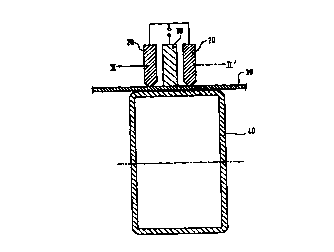
As shown in Fig. 1, the resistance assembly according to the invention can be
used for assembling sheet metal and hollow bodies 40 with sheet metal 30.
Here,
for instance, a 0.8mm thick ST37 sheet metal is placed in welding position on
an
ST37 hollow body 40 with a wall thickness of 2.5 mm manufactured through
internal high-pressure metal forming. All electrodes 10,20 are brought in
electric
contact with the outer surface of the sheet metal 30 on top, with the internal
electrode being surrounded by two counterelectrodes 20, which are formed here
in a circular segment . (Of course, any other form, through which the internal
electrode is surrounded by counterelectrodes to avoid the migration of
current,
without getting in contact with the outer electrode, is possible). Here, a
copper
alloy, namely CuCr Zr, was used as electrode material, in order to achieve
optimal electrical as well as thermal conductivity for a good service life. Of
course, other materials that conduct electricity well, which are known to the
expert, can be used for the electrodes. After applying a welding arc voltage
to
the electrodes and the welding current has flowed through the parts to be
assembled, that are between the electrodes with different polarity in the
environment of the central electrode, a resistance welding process is
introduced,
with the path of the current corresponding only to about the distance between
the
central electrodelcounterelectrodes plus the sheet thickness. In the process,
pressure can be applied axially on the electrodes) 20 to support the welding
process. Parts 30, 40 for assembly can be defined in this manner and
assembled with one another in uniform quality.
CA 02310025 2000-02-14
WO 99/08825 PCT/DE98/02091
or the like, may be placed between the electrodes to avoid an undesired
voltage
flash-over between the two electrodes. However, in most cases, insulation
through air or gas is sufficient. The expert is familiar with appropriate
materials.
A further possible arrangement of the electrodes is shown in Fig. 3. Here, two
electroconductive parts are supposed to be assembled with one another in their
edge area. Counter and central electrodes 10,20 can be arranged here on the
edge, and the direction of the flow of current can be improved even more
through
a good, conductive material placed under the sheet metal, thereby ensuring an
exact and good welding of the sheet metal in the edge area after the welding
or
soldering voltage is applied (if there is soldering material in between, the
assembly process can again be introduced, the path to be covered by the
current
only roughly corresponding to the distance of the two electrodes 10,20 plus
the
material thickness. An insulating material, if required, can in turn be placed
between the two electrodes.
Figure 4 illustrates an application according to the invention on tube parts
for
fitting into one another. Here, the central electrode 10 as well as the two
counterelectrodes 20, which have a small contact surface here, are placed on
the
outer tube. The welding current then flows between the central electrode and
the
counterelectrodes while assembling the two hollow parts fitted into one
another.
As illustrated in Fig. 5, the resistance welding assembly according to the
invention can be used to assemble hollow bodies 40 with sheet metal 30. Here,
the sheet metal is perforated with or without necking/welding hump and placed
by the hollow body 40 in welding position. Through the hole 60, an initial
electrode10 is introduced in such a way that it contacts the outer surface of
the
hollow part 40 behind it, without touching the overlying part 30. The second
electrode 20, which is shaped here as a hollow cylinder (of course, any other
hollow form, through which the inner electrode can be moved without coming
into
contact with the outer electrode, is possible) is axially pushed beyond the
first
electrode 10 until it has contact with the surface of the perforated sheet
metal 30
beside the opening. After applying welding voltage to the electrodes and flow
of
the. welding current through the parts for assembly in the environment of the
hole,
a resistance welding procedure is introduced, with the path of the current
only
corresponding roughly to the radian difference of the two electrodes plus the
sheet metal thickness. To support the welding process, pressure can be applied
a CA 02310025 2000-02-14
WO 99108825 PCT/DE98/02091
requirement and base material and requirements of assembly temperature and
type of assembly.
Fig. 6 illustrates a further, possible arrangement of the electrodes. This
involves
a "stick electrode" 10, around which the second electrode 20 is shaped as a
hollow cylinder. Here, it is important for the feed of the electrodes 10, 20
to be
variable so that parts of different thicknesses can be assembled with one
another. There is insulating material, such as ceramic, porcelain or the like
between the electrodes, in order to avoid an unwanted voltage flash-over
between the two electrodes. The expert is familiar with appropriate materials.
Fig. 7 illustrates a further, possible arrangement of the electrodes. Two
electroconductive parts are supposed to be assembled with one another here,
for
instance in their edge area. It is advantageous when the "lower"
electroconductive part projects over the "upper" electroconductive part a
little.
The front electrode 10 can now be placed on the "upper" part and the rear
electrode 20 can be placed on the "lower" part, and after applying welding or
soldering voltage (if soldering material is placed in between, the assembly
process can be introduced once again, the path to be covered by the current
roughly corresponding to the distance of the two electrodes 10, 20 plus the
material thickness2. Insulation material, if required, can in turn be placed
between
the two electrodes.
Further developments are obvious to the expert within the scope of the extent
of
the protection of the claims, and the extent of the protection is not at all
limited,
for instance, to the embodiments cited here, which merely serve to illustrate
the
invention.