Note: Descriptions are shown in the official language in which they were submitted.
CA 02310508 2000-06-O1
' ~ 17422CA
Circuit For Dual Band Tuning
Field Of The Invention
The invention relates to a circuit that is
switchable to different frequency bands, and to a circuit
that is digitally switchable to different frequency bands
by changes in reactive circuit elements of the circuit.
Background Of The Invention
Wireless telephones operate in more than one
frequency band, for example, Cellular 900MHz and PCS 1900
MHz. In the past, to operate in more than one frequency
band, a separate, narrow band, RF circuit was provided
for each of the different bands. The advantage was that
each narrow band circuit could be tuned precisely for
optimum performance within its tuned frequency band. A
disadvantage resided in the relatively large collective
sizes of the individual circuits, which restrained the
ability to make wireless phones smaller. Further, since
the addition of each frequency band required an
additional tuned circuit, manufacturing costs were
increased. Further, switching among the separate circuits
required an external switch, a switch that was external
to the RF tuned circuits. An external switch increases
manufacturing cost, and operates slowly in an external
circuit.
As described in U.S. Patent 3,611,154, a known
circuit that is switchable to different frequency bands,
for example, UHF and VHF bands, has a local oscillator
with a transistor that is biased by a bias voltage
applied at a point designated "A" to an LC (inductance,
capacitance) resonant circuit connected between the base
and collector of the transistor. The resonant circuit is
referenced to ground or earth. A varicap diode in the
resonant circuit has its capacitance varied by the value
of its bias voltage, which allows tuning of the resonant
circuit of the local oscillator for resonance with a
first frequency band, UHF, for example. To switch to a
Page 1
CA 02310508 2000-06-O1
' 17922CA
second frequency band, VHF, for example, a switching
diode starts conducting. The switching diode is connected
at the junction of two inductors in the LC resonant
circuit, and is biased to a conducting state by a
switching voltage applied at a point designated "S".
There are DC blocking capacitors between earth and the
switching diode, such that when a double throw switch is
thrown to apply the switching voltage to the diode, the
diode is biased to a conducting state, causing current to
flow through one of the inductors to ground. Thereby, one
of the two inductors becomes shorted to ground, which
tunes the resonant circuit for resonance with the second
frequency band.
Disadvantages of the known circuit reside in the
double throw switch, which is external to the RF tuned
circuit. The RF tuned circuit must be manufactured with
the switch as an external component. Further, the switch
is slow to operate as it is external to the RF tuned
circuit. The known circuit is further disadvantageous as
having an ECL biased transistor, which is not suitable
for low voltage operation. The double throw switch of the
known circuit in the off position is shunted to ground
through a resistive load in parallel with a Zener diode,
which dissipates current, and which is unsuitable for use
in a low voltage device, such as, a dual frequency band,
personal communications unit.
Another known circuit switchable to different
frequency bands is described in U.S. Patent 4,379,269.
The known circuit has an FET transistor in which one gate
is supplied by a bias voltage and a second gate is fed
with a uniform voltage by an automatic gain control, AGC.
A voltage that is used as the bias voltage is divided at
a voltage dividing point. A switching voltage is used to
switch to different frequency bands. The switching
voltage is supplied to a switching diode. The switching
diode conducts and shorts an inductor of a resonant
Page 2
CA 02310508 2000-06-O1
' ~ 17422CA
circuit to ground. The switching diode feeds the
switching voltage at the voltage dividing point, which
raises the voltage at the dividing point upon the
reception of a high frequency band. Upon selection of a
low band a bias voltage is applied to the switching
diode, which back biases the diode. The diode ceases to
conduct, and the inductor of the resonant circuit is no
longer shorted to ground. At the same time, the bias
voltage is applieE3 to a voltage dividing circuit and is
impressed as the bias voltage upon the first gate of the
FET, which tunes the RF circuit to a lower frequency
band. The FET has its AGC delayed if the bias voltage to
the first gate is lowered. The FET has its AGC advanced
if the bias voltage at the first gate is made higher. A
disadvantage of the known circuit is its unsuitability
for a low voltage application, such as personal
communication devices, because the switching diode is a
discrete circuit element requiring significant voltage
for its bias, either forward or backward bias. Further,
the switching diode is an active device having its own
characteristics as a reactive element with capacitance
and inductance values that deter the precise tuning of
the resonant circuit to different frequency bands.
Summary Of The Invention
The invention relates to dual band matching by
either a dual band inductance circuit or a dual band
capacitance circuit. The invention allows many of the
same circuit elements and functions to be used in
different frequency bands without significant performance
degradation or increase in size. The invention utilizes
matching circuit networks capable of precise tuning to
multiple frequency bands. According to an embodiment of
the invention, MESFET switches are integral with the
tuning circuits, which enables fast switching response
and low voltage operation, as opposed to known circuits
having external switching devices, such as, a double
Page 3
CA 02310508 2000-06-O1
'- 17422CA
throw switch and a switching diode, as described by the
above referenced patents. The MESFET switched circuits
according to the invention are fabricated as part of the
tuning circuit, and are of lower inherent impedances than
discrete switching devices, which enables precise tuning
to multiple frequency bands. The MESFET switched circuit
is adaptable for dual band tuning of reactive element
tuning circuits, including dual band inductance circuits
and dual band capacitance circuits.
Description Of The Drawings
Embodiments of the invention will now be described
by way of example with reference to the accompanying
drawings, according to which:
Figure 1 is a schematic view of a dual band RF
tuning circuit:
Figure 2 is a schematic view of another embodiment
of a dual band RF tuning circuits and
Figure 3 is a schematic view of another embodiment
of a dual band RF tuning circuit.
Detailed Description
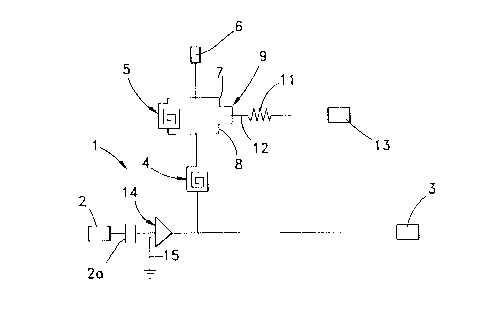
With reference to Fig. 1, a dual band RF tuning
circuit 1 is in the form of a dual band inductance tuning
circuit connected between an RF input port 2 and an RF
output port 3. The input port 2 receives an input RF
signal of a selected frequency band. The input port
includes a DC blocking capacitor 2a. Tuning is provided
by a first impedance element 4 in the form of an
inductance impedance element having a first inductance La
and a second impedance element 5 in the form of a second
inductance element having a second inductance Lb . The
impedance elements 4, 5 are in series connection with a
reference voltage port 6 receiving an input, low voltage
Vref , for example, 2 . 7 volts .
The second impedance element 5 is in parallel
connection with two conducting gates 7, 8 of a switching
transistor 9, for example a MESFET switching transistor.
Page 4
CA 02310508 2000-06-O1
- ' ' 17422CA
A relatively large, current blocking resistance 10, for
example, 5K Ohms, is in parallel connection with the
second impedance element 5. Further, the two conducting
gates 7, 8 of the switching transistor 9 are in parallel
connection with the resistance 10 that serves as a
biasing resistor that maintains the two conducting gates
7, 8 at the same potential. A similar biasing resistor 11
is connected at the gate 12 of the switching transistor
9.
When the switching transistor 9 is nonconducting, or
switched to off, the first and second impedance elements
4. 5 are conducting. The tuning impedance of the circuit
1 is the sum of the first inductance La and the second
inductance Lb. The circuit 1 is tuned to a first input RF
signal at a first bandwidth, and the RF signal of the
first bandwidth is provided at the RF output port 3.
The switching transistor is biased on and off,
conducting and nonconducting by changing its bias
voltage. The conducting gates 7, 8 of the switching
transistor 9 are connected to the second impedance
element 5 to short the second impedance element. More
specifically, the gate 12 of the switching transistor 9
is biased by a band control voltage source 13 that
supplies a band control voltage Vdd through the biasing
resistor 11 at the gate 12 of the switching transistor 9,
causing the switching transistor 9 to conduct and short,
or bypass, the second inductance impedance element 5.
Accordingly, with the switching transistor 9 conducting,
or switched to on by the band control voltage, the tuning
impedance of the circuit 1 is due to the first impedance
element 4 alone. The circuit 1 is tuned to a second input
RF signal at a second bandwidth, and the second RF signal
is passed by the conducting swithing transistor 9 and is
provided at the RF output port 3.
Further, for example, the input RF signal is
supplied first to an amplifier 14 at the RF input port 2.
Page 5
CA 02310508 2000-06-O1
17422CA
The amplifier 14 is referenced to ground at 15 in a
manner to be described in conjuction with Fig. 3.
With reference to Fig. 2, another embodiment of the
dual band RF tuning circuit 1, in the form of a dual band
capacitance tuning circuit, will now be described. The
circuit 1, of Fig. 2, comprises a first impedance element
4 in the form of a capacitance impedance element of
capacitance Ca between the input port 2 and the output
port 3. A second impedance element 5, comprises series
connected, two capacitance impedance elements 5a, each
having capacitances Cb . The second capacitance impedance
element 5, of Fig. 2, is in parallel connection with the
first capacitance impedance element 4.
The current blocking resistance 10, of Fig. 2, is
provided by a voltage divider having two biasing
resistors l0a connected at a voltage dividing point 17.
Each biasing resistor l0a has a resistance value of 5K
Ohms, for example. The band control voltage source 13 is
connected through a similar resistor lOb to the voltage
dividing point 17. The voltage divider is in parallel
connection with the conducting gates 7, 8 of the
switching transistor 9. The resistors l0a are of equal
resistive value to maintain the conducting gates 7, 8 at
the same potential. A similar biasing resistor lOc
connects at the gate of the switching transistor 9 and is
referenced to ground 15.
The switching transistor 9, of Fig. 2, is connected
to the second capacitive impedance element 5, to short
the second capacitive impedance element 5. More
specifically, the conducting gates 7, 8 of the switching
transistor 9 are in series connection with, and between
the two capacitance impedance elements 5a, of Fig. 2.
When the switching transistor 9 is switched on, or
conducting, the capacitance of the circuit 1 is the
mathematical sum of the first capacitance Ca plus ~ of the
capacitance Cb . Accordingly, the circuit 1 is tuned to a
Page 6
CA 02310508 2000-06-O1
' 17422CA
first input RF signal at a first bandwidth, and the
conducting swithing transistor 9 passes the first input
RF signal to the RF output port 3. The switching
transistor 9 is turned off by having the gates biased to
the same potential by the band control voltage Vdd
supplied at a low voltage value, for example 2.7 volts,
at the voltage dividing point 17. Turning off the
switching transistor 9, means that the switching
transistor 9 shorts or bypasses the two capacitance
impedance elements 5a that comprise the second
capacitance impedance 5, which switches the capacitance
of the circuit 1 to the value of the first capacitance Ca
. Accordingly, with the switching transistor turned off,
or nonconducting, tuning circuit 1 is tuned solely by the
first capacitive impedance element 4 alone. Thereby, the
tuning circuit 1 is tuned to an input RF signal at a
second bandwidth. For example, the input RF signal is
amplified by the amplifier 14.
With reference to Fig. 3, an embodiment of the
amplifier 14 will now be described. An input RF signal is
supplied through the DC blocking capacitor 2a to the gate
16 of a MESFET transistor 18. A voltage divider having
two similar resistances 19 are connected between the gate
16 and one of the conducting gates 20 of the transistor
18. A broadband RF extractor Balun has an inductor 21
connected to the voltage division point of the voltage
divider. The amplifier 1 is referenced to ground 15 at
the division point of the voltage divider.
With further reference to Fig. 3, the output of the
amplifier 14 is supplied to the input side of the RF
tuning circuit 1 that comprises either the inductive
tuning circuit, as described and shown in Fig. 1, or the
capacitive tuning circuit, as described and shown in Fig.
2. Further, the RF signal is supplied, according to
another embodiment, to both of the tuning circuits 1
simultaneously, as in Fig. 3, to provide even greater
Page 7
CA 02310508 2000-06-O1
' 17422CA
precise tuning by both an inductive tuning circuit and a
capacitive tuning circuit. Not only is there redundancy
should one circuit 1 becomes inoperative, but also, both
tuning circuits 1 are operative simultaneously to
compensate for stray capacitance and/or stray inductance
from external sources of RF signal interference.
With further reference to Fig. 3, the second
inductance impedance element 5 is in parallel connection
with a further capacitance 20 to obtain a larger
effective inductance.
The switching transistor 9 has a negligible
impedance, permitting precise tuning of each embodiment
of the tuning circuit 1 to the optimal narrow band
performance. The embodiments of the tuning circuit 1
respectively maintain their DC characteristics of each
inductor and capacitor, which avoid adverse impact on the
biasing of external active devices in RF circuits.
Further, the switching transistor 9 is switched with a
low voltage, adapting the embodiments of the tuning
circuit 1 for low voltage operation. Further, the
switching transistor 9 is digitally switched with quick
response to change the RF tuning band. Further, the
switching transistor 9 is integrated into each embodiment
of the tuning circuit 1, as a single integrated circuit,
MMIC, avoiding a requirement for an external discrete
device to do the switching. Further, the switching
transistor 9, as well as its biasing resistors and the
other reactive circuit elements of each of the tuning
circuits, are readily fabricated in small sizes when
fabricated on an MMIC as a single unit. The combined
ability to change inductance and capacitance, the
preservation of low voltage DC switching operation, and
the simplicity and small size of the invention enables
fabrication of a multiple band RF switching device in a
single MMIC.
Page 8
CA 02310508 2000-06-O1
17422CA
Other embodiments and modifications of the invention
are intended to be covered by the spirit and scope of the
appended claims.
Page 9