Note: Descriptions are shown in the official language in which they were submitted.
CA 02310856 2000-06-06
Time-Slotted Optical Space Switch
Abstract
A method and apparatus for the switching synchronised bursts lcal signals
arnving
at a multiplicity of input ports and destined to distinc ut ports is
disclosed. A basic
switching unit is disclosed that transfers n ' optical signals to n distinct
output signals
under the control of digital electr signals. Apparatus and methods for
building n by n
basic switching units be reconfigured at high rates are disclosed. Methods are
disclosed for mg larger N input by N output optical switches by
interconnecting and
co mg arrays of basic switching units. Methods are disclosed for the
allocation of
transmission capacity across said optical switches.
Field of Invention
The present invention in general relates to optical switches used in
telecommunications
and computer networks to switch and route optical signals arnving in one or a
plurality of
input ports to one or a plurality of output ports.
Optical transmission technologies have increased the information-carrying
capacity of a
single optical fiber to more than 1 Terabit per second. Future switches must
therefore be
able to transfer aggregate information rates in the many Terabits per second.
Electronic
switches that can handle these information rates are extremely difficult to
build because
of the relatively-limited information-carrying capacity of electronic systems.
Optical
switches that transfer information in optical form can avoid the bottleneck
inherent in
electronic switches.
Time slot exchange is a basic approach in the design of systems for
transmitting and
switching information. The time-division multiplexed telephone network and the
SONET/SDH transport networks are both organized around a 125 microsecond time-
slot.
ATM and related network technologies are designed around the notion of fixed-
length
units of information. The time-slot approach introduces modularity in the
units of
information that need to be handled and processed and through synchronization
of time
slots allows parallel and high-speed operation.
More specifically, the present invention relates to time-slotted optical
switches that are:
1. modular in design and can be built from small to large number of port
counts; 2.
flexible in the type of optical signals that can be carried, from single
wavelengths, to
bands of wavelengths, to broad regions of optical spectrum; 3. reconfigurable
in terms
of the allocation of transmission opportunities to different input-output port
pairs. The
present invention can be used to build optical and electronic switches and
routers in
telecommunications and computer networks.
Discussion of Previous Art
The transmission of information over optical fiber systems provides the
advantages of
extremely high transmission rates (measured in bits per second) and extremely
low bit
error rates. The design of electronic switches to transfer information among
optical fiber
CA 02310856 2000-06-06
systems is very challenging because of the extremely large volumes of
information that
must be handled electronically. All-optical switches transfer information
among optical
fiber systems without converting the information streams into electronic form,
and hence
avoid the electronic bottleneck inherent in electronic switches.
Optical switches can categorized according to whether the transfer of
information is
controlled using the space, time, or wavelength domains. In the case of space
switches,
the optical signals that arrive in an input port are routed along disjoint
paths through the
switch to the desired output ports. Space switches are typically built from
arrays of
crosspoints that direct the signal across the switch. Multistage arrangements
of small
space switches can be used to produce space switches with a large number of
parts.
Benes and Clos multistage switches are preferred because of their non-blocking
properties, that is, the ability to provide connections from any idle input to
any idle
output.
Space switches can be used to provide long-term connections (of duration
seconds or
more) between input ports and output ports. During the term of the connection,
the
optical signal can flow continuously from input to output. The transfer of the
optical
signal is said to be transparent because the manner in which information is
modulated and
formatted is not relevant to the operation of the switch. Micro-
electromechanical systems
(MEMS) are an example of such space switches.
In wavelength switches, composite optical signals arrive at each input port.
Each
composite signal consists of the combination of several optical signals, each
using a
distinct wavelength from some preselected set of allowable wavelengths. The
wavelength switch separates the composite optical input signals according to
wavelength,
and it uses a separate space switch to transfer the set of inputs at each
given wavelength
to their desired output ports. The outputs from the various space switches
directed to a
given output port are then wavelength division multiplexed into a composite
optical
signal that exits the switch. Wavelength switches can be used to provide end-
to-end
transparent connections consisting of a single wavelength between two points
in a
network.
In time switches, the optical signals that arnve at each input port consist of
a sequence of
signal bursts, of some fixed duration called a "time slot". Each burst at an
input port
must be routed independently across the switch. A space switch that can be
reconfigured
rapidly can be used to build a time slot switch. At periodically recurring
time instants,
the switch is reconfigured so that it connects input ports to output ports
according to
some desired permutation arrangement. No valid signal information is allowed
into the
switch during the reconfiguration time, so a guard time is used to separate
the bursts of
optical signal that traverse the switch. The time slots that arrive at
different input ports
need to be synchronized so that they enter the switch at the same time, right
after the end
of the guard time. Time-slotted switches allow the transfer of optical
information from
any input port to any output port over relatively short time intervals, in the
order of
microseconds, and in effect support the simultaneous transfer of information
among all
ports in the switch.
2
CA 02310856 2000-06-06
The synchronization of the optical bursts that enter the time-slotted switch
can be carried
out in a straightforward fashion if the optical signals are generated (or
regenerated)
locally in the line cards that feed the switch. The synchronization of optical
bursts that
arrive from some distant system requires the use of burst alignment techniques
such as
those discussed in [Guillemot 1998, pg. 2130].
There are two fundamental approaches to the transfer of information in a
network. The
first approach involves the setting up of relatively long-lived circuits that
enable the flow
of information between two points in the network. The second approach involves
the
transfer of information in the form of packets. Both of these approaches can
be supported
by time-slotted switches.
In the case of long-term circuits, the time-slotted optical switch can be
configured to
provide a periodic transfer of bursts of optical signal from specific inputs
to specific
outputs according to some fixed schedule. The schedule ensures that each
connection
receives the desired rate of information transfer. A connection admission
procedure is
required to ensure that the switch is capable of supporting a new request for
a circuit, and
then to set up the desired transfer of time slots in the switch permutation
schedule.
Time-slotted optical switches can also be operated to transfer individual
packets or blocks
of information that fit within a single time slot. In this case, the
configuration of the
space switch must be controlled dynamically according to the pattern of packet
requests
at the input to the switch.
Hybrid approaches that combine a fixed schedule to accommodate circuit
connections
and dynamic scheduling to accommodate short-lived packet traffic are highly
desireable
given the variability in volume and locality of Internet traffic. One hybrid
approach
involves the use of a frame structure in which some time slots are allocated
on a longer-
term basis to circuits while other time slots are allocated dynamically to on-
demand
traffic. Many allocation algorithms are possible according to what criteria is
used in
making the allocation and how quickly the adaptation to on-demand traffic is
carried out.
The present invention discloses methods and apparatus for a time-slotted
optical switch
that can provide circuit or on-demand transfer of bursts of optical signals
from input ports
to output ports. The invention is based on a space switch disclosed in Patent
Application
# xyz, "A Modular, Expandable and Reconfigurable Optical Switch," by Leon-
Garcia et
al. Said space switch is composed of an array of basic space switching units
that are
constructed from electrooptic wafer beam deflection switch components. The
time to
reconfigure the basic space switching units and the overall space switch is
limited
essentially by the speed of the control voltage driver circuit, currently in
the order of
100's of nanoseconds. The space switch can be operated in time-slotted fashion
with
time slots set to several microseconds.
Current optical transmission systems have an inherent information transmission
capacity
in excess of 1 Terabit per second, but the digital modulation systems
currently available
3
CA 02310856 2000-06-06
can only handle information in the tens of Gigabits per second. In order to
use the large
inherent capacity of optical fiber, wavelength division multiplexing (WDM)
systems
combine multiple independently modulated optical signals of different
wavelengths into a
single combined optical signal that can be transmitted in a single optical
fiber. WDM
thus provides a means of packing extremely high volumes of information
transfer in
small regions in space.
The space switch disclosed in Patent Application # xyz, "A Modular, Expandable
and
Reconfigurable Optical Switch," by Leon-Garcia et al, has the property that it
can
transfer a broad range of wavelengths of an optical signal. Consequently, the
space
switch has a very large inherent information transmission capacity, much as in
the case of
optical fiber. The present invention discloses methods that use WDM to exploit
this
inherently high information transfer capability and to in effect provide a
switch with a
larger number of input and output ports.
Summary of Invention
The present invention presents a method and apparatus for time-slotted optical
switches
that transfer bursts of optical signals arriving at a multiplicity of input
ports and destined
to distinct output ports. A basic switching unit is disclosed that transfers n
input optical
signals to n distinct output signals and that can be rapidly reconfigured
under the control
of digital electronic signals. A preferred embodiment of the basic switching
unit using an
electrooptic wafer beam deflector component is disclosed. Also disclosed is a
modular
approach for building large time-slotted optical space switches using basic
switching
units as building blocks. Methods for allocating the transmission capacity to
different
input-output flows as well as to circuit and on-demand traffic are also
disclosed. Finally
a method for expanding the number of switch ports using wavelength division
multiplexing is disclosed.
Brief Description of the Drawings
Figure 1 nxn basic switching unit with active splatters and active combiners
Figure 2 nxn basic switching unit with active sputters and passive combiners
Figure 3 Timing in time-slotted space switch operation
Figure 4 Switch fabric and associated control unit
Figure 5 16x16 Benes Switch using identical basic switching units
Figure 6 16x16 Benes Switch using multiple size basic switching units
Figure 7 Clos strictly non-blocking switch
Figure 8 Time-slotted space switch
Figure 9 TDM sequence of interconnection matrices & switch configurations
4
CA 02310856 2000-06-06
Figure 10 Sequence of interconnection matrices for unbalanced and nonuniform
traffic matrix
Figure 11 Expanded optical switch using wavelength division multiplexing
Detailed Description of the Invention
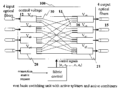
Figure 1 shows a 4x4 example of an nxn basic switching unit 100 constructed
from n 1 xn
active sputters 20 and n nxl active combiners 21. A single output fiber 10
from each
active splitter is connected to an input 11 of each of the active combiners.
The control
voltage 12 in each active sputter directs the input optical signal to the
desired output fiber
and thereafter the optical signal propagates to the corresponding active
combiner. The
10 active combiner directs the single arnving optical signal to the output
fiber 15 under the
control of a voltage signal 16.
A switch unit control 30 associated with the nxn basic switching unit in
Figure 1 takes the
control signal generate by a central controller (of the overall time-slotted
space switch)
and generates control signals c; that are distributed to the control circuitry
associated with
each splitter/combiner. Said control signal c; specifies one or more voltage
levels which
are applied in the splitter/combiner to produce the desired deflection in the
beam and
effect the desired routing from a given input fiber to a desired output fiber.
A consistent set of control voltage signals is required in the nxn basic
switching system in
Figure 1 to direct each of the n input optical signals to a distinct output
port. The nxn
basic switching unit is then equivalent to a crossbar switch in the sense that
it can direct
any of n input signals to any output port that is not already in use.
Figure 2 shows a 4x4 example of an nxn basic switching unit 200 constructed
using n 1 xn
active sputters 47 and n nxl passive combiners 48. A single output fiber 40
from each
active splitter is connected to an input 41 of each of the active combiners.
'The control
voltage 42 in each active splitter directs the input optical signal to the
desired output fiber
43 and thereafter the optical signal propagates to the corresponding passive
combiner.
The passive combiner combines all arnving optical signals and a portion of the
energy in
the arriving optical signal appears at the output fiber 45. The system in
Figure 2provides
an acceptable basic switching unit as long as the output signals have an
adequate signal-
to-noise ratio.
A preferred embodiment of the active splitter and active combiner in Figure 1
and in
Figure 2 involves the use of electrooptic wafer beam deflectors as disclosed
in U.S.
Patent #xxx and Patent Application # xyz, "A Modular, Expandable and
Reconfigurable
Optical Switch," by Leon-Garcia et al.
A preferred embodiment of the control signals c; in Figure l and in Figure 2
where c;
specifies whether a deflection voltage is on or off in each of the multiple
prism segments
in a substrate as disclosed in Patent Application # xyz, "A Modular,
Expandable and
Reconfigurable Optical Switch," by Leon-Garcia et al. The driver circuitry for
5
CA 02310856 2000-06-06
producing the binary deflection voltages can effect the reconfiguration of the
beam
deflection in sub-microsecond time intervals [IR 2000].
The operation of the basic switching units of Figure 1 and Figure 2 as time-
slotted optical
space switches involves the repetition of a cycle of events as shown in Figure
3. Each
cycle is T seconds in duration.
As shown in Figure 3, the first tco~g seconds in each cycle provide a guard
time during
which the control signals are distributed to the active splitters and
combiners and the
associated deflection voltages are applied. At the end of t~o~g seconds each
optical beam
is deflected from the specified input to the corresponding desired output.
During the
guard time interval, any optical beams present at the inputs may propagate to
various
outputs in uncontrolled fashion producing a form of crosstalk. Indicator
signals are
available at the output of the switches to indicate that the optical signal at
the output ports
is not valid during the guard time interval.
The end of the guard time interval in Figure 3 is followed by the dwell-time
interval of
duration tdWeii seconds. At the beginning of the dwell-time interval, the
input ports are
given a signal indicating that switch is ready to switch the bursts of input
optical signals.
During this interval, the space switch maintains a specific interconnection
pattern
directing optical signals from given input ports to specific corresponding
output ports.
The bursts of input optical signals are then transferred to the desired output
ports.
The time-slotted optical space switches of Figure 1 and Figure 2 can operate
as in
standalone mode and provide transfer of burst of optical signals from their n
input ports
to their n output ports. Time-slotted optical space switches of dimension nxm
can be
obtained by taking a basic switching of a given size and not using some of the
input or
output ports.
Physical constraints limit the maximum size n of an active sputter or an
active combiner.
This in turns places a maximum size on the number of ports in a basic
switching unit.
Traditional switching theory derived from telephony networks provides methods
for the
construction of large NxN space switches from modules consisting of smaller
space
switches [Stern 1999, pg. 39]. These constructions typically involve an array
of multiple
switches of various sizes. The outputs of the switches in a given stage are
connected to
inputs of switches in the next stage in order to provide a number of
alternative paths from
the inputs to the outputs of the NxN switch.
Figure 4 shows how the configuration of a large NxN switch is controlled by a
switch
fabric control unit. Figure 4 shows the multiple stages of modules that
constitute the large
NxN switch. (Note that the figure does not show the interconnections between
the
various stages.) A switch fabric control accepts requests for a given set of
connections
from given inputs to specific outputs. The switch fabric control executes an
algorithm
that is specific to the particular multistage construction to determine what
internal
configuration of connections within the modules will realize the requested set
of
connections. The switch fabric control then distributes digital control
signals to the
6
CA 02310856 2000-06-06
modules specifying their internal configuration. The desired set of
connections becomes
available when the modules complete the reconfiguration specified by the
control signals.
Time-slotted optical space switches of large dimension NxN can be constructed
from
basic switch units of size nxm as modules and using multistage constructions.
The
operation of said NxN switches must also operate in cycles of the form shown
in Figure
3. Prior to the beginning of each reconfiguration interval, the fabric switch
control must
determine the set of internal connections in the basic switching units to
achieve the
required set of connections from the inputs to the outputs of the NxN switch.
During the
reconfiguration interval, the control signals are distributed to the basic
switching units
which in turn reconfigure their internal set of connections. At the end of the
reconfiguration interval, the NxN space switch is ready to transfer bursts of
optical
signals from given inputs to specified outputs.
The Benes and Clos multistage constructions are of particular interest because
of their
nonblocking properties. Figure 5 shows an example of how a 16x16 optical
switching
fabric 300 can be constructed from three stages of 4x4 basic optical switching
units as
disclosed in Patent Application # xyz, "A Modular, Expandable and
Reconfigurable
Optical Switch," by Leon-Garcia et al. More generally, given an nxn basic
switching
unit constructed as shown in Figure f or in Figure 2, it is possible to
construct and n2 x n2
larger switching fabric using a three-stage construction using the
interconnection
approach described above. In general an n2 x n2 three-stage Benes construction
requires
3n basic switching units. A five-stage n3 x n3 Benes construction for a large
switch is
also possible. In general said n3 x n3 five-stage Benes construction requires
Sn2 basic
switching units. More generally, an nk x nk (2k-1)-stage Benes construction
requires (2k-
l )nk-I basic switching units.
A preferred embodiment of the present invention involves the construction of
n2 x n2 and
n3 x n3 Benes constructions of optical switching fabrics using the basic nxn
switching
units shown in Figure l and in Figure 2. The corresponding three- and five-
stage
switches are feasible because of the low loss property of the basic switching
units
constructed using electrooptic wafer beam deflector components.
The Benes method also allows the construction of large optical switching
fabrics from
smaller basic switching units of several sizes. Figure 6 shows a three-stage
16x16 optical
switch fabric 400 constructed from first and third stages consisting of 8 2x2
basic
switching units 61 and a central stage consisting of 2 8x8 basic switching
units 62. In
general, an NxN switches can be constructed in three stages or in five stages
if N can be
factored as the product of two or three whole numbers, respectively.
A preferred embodiment of the present invention for a time-slotted optical
space switch
involves the construction of three and five stage Benes optical switching
fabrics using
basic switching units shown in Figure 1 and Figure 2. The corresponding three-
and five-
stage switches are feasible because of the low loss property of the basic
switching units
constructed using electrooptic wafer beam deflector components.
7
CA 02310856 2000-06-06
The Benes switch fabric constructions described above are "rearrangeably non-
blocking"
in the sense that they can realize any interconnection pattern of any N inputs
to any N
distinct outputs, but the addition of a new connection to an existing set of
fewer than N
existing connections may require the re-arrangement of all connections. This
non-
blocking property of the Benes switch fabric constructions indicate that the
switch fabric
control in Figure 4, when implementing appropriate algorithms, can always find
a set of
internal connections for each constituent switching module to connect the
inputs to an
arbitrary set of distinct outputs.
[Clos 1953] developed a method for constructing non-blocking multi-stage
fabrics that do
not require rearrangement of existing connections when a new connection is set
up. The
basic Clos construction for an NxN switch consists of three-stages. The first
and third
stages consist of k rows of pxm basic switching units, and the central stage
consists of m
k x k basic switching units. It is well-known that if m=2p-1, then the Clos
switch fabric is
strictly non-blocking in the sense that existing connections do not need to be
rearranged
to establish a new connection from an available input to an available output.
Figure 1
shows an example of an 8x8 non-blocking Clos switch 800 constructed from 2x2
and 4x4
basic switching units. In this example, p=2, k=4 and m=2p-1=3. Clos switch
fabrics can
be operated in time-slotted mode using the control approach discussed with
Figure 4.
A preferred embodiment of the present invention is a three-stage arrangement
of a Clos
switching fabric in which the basic switching units are constructed using
electrooptic
wafer beam deflector components.
When a large NxN time-slotted optical space switch shown in Figure 8 is built
using a
Clos or Benes construction, then the NxN switch operates as if it were an NxN
crossbar
switch that can implement any permutation of connections from inputs to
outputs. The
configuration of said switch during cycle t is specified by a matrix P(t) _
{p;~(t)), where
p;~(t) is equal to 1 if input i is connected to output j, and is equal to zero
otherwise. P(t)
has the property that each row has exactly one non-zero value, and each column
has
exactly one non-zero value. The sequence P(1), P(2), P(3), P(4), ... represent
the
sequence of interconnection patterns provided by the NxN switch. The number of
times
the ijth component equals 1 in the sequence P(1), P(2), ..., P(k) represents
the number of
time slots allocated to connection ij in k consecutive cycles. Hence the
allocation of
transmission opportunities ("bandwidth") among input-output pairs is
determined by the
sequence of configuration matrices.
The sequence of interconnection patterns P(1), P(2), P(3), P(4), ... can be
selected to
meet the bandwidth requirements of the traffic that traverses the switch. In
the case
where the same level of traffic flows between every input and output port and
where the
traffic flows are relatively steady, a suitable sequence consists of a
repetitive
interconnection pattern P( 1 ), P(2), . . . , P(N-1 ), P(N), P( 1 ), P(2), . .
., P(N-1 ), P(N), . . .
that provides every input-output pair with 1 transmission opportunity per
repetition cycle.
We refer to said repetitive pattern as a Time-Division Multiplexing (TDM)
schedule.
Figure 9 shows an example of such a repetitive pattern for a 4x4 switch: A
repetitive
pattern of 4 permutation matrices and the associated switch configurations are
shown.
8
CA 02310856 2000-06-06
Note in this example that the sequence uses only 4 of the 4!=24 possible
permutation
matrices. Note also that different sequences of permutation matrices can be
used to
produce TDM schedules.
In the case where different levels of traffic flow between different input and
output ports
and where the traffic flows are relatively steady, a suitable schedule
consists of a
repetitive interconnection pattern P(1), P(2), ..., P(N-1), P(N), P(1), P(2),
..., P(N-1)
P(N), ... that provides an input-output pair with a number of transmission
opportunities
per repetition cycle that is proportional to the relative traffic flow of the
input-output pair.
Figure 10 shows an example of a traffic matrix for a 4x4 switch and a
corresponding
repetitive interconnection pattern that satisfies the traffic demand. The ijth
entry in the
traffic matrix is the proportion of time information is available for transfer
from input
port i to output port j. The "x" in the permutation matrices in the figure
denote "don't
cares" for connections in the switch that have not been assigned. Various
algorithms are
available for synthesizing an repetitive interconnection pattern for a given
traffic matrix
[Algoxxx].
The interconnnection pattern can be modified over time to track variations in
traffic
levels and to deal with temporary surges in traffic. By keeping a running
average of the
traffic flow between each input-output pair, the variation in the traffic
matrix can be
tracked and adjustments in the interconnection pattern can be made. These
adjustments
may consist of small changes in the permutation matrices or in the repetitive
pattern itself
through the addition or deletion of one or more permutation matrices. Surges
in traffic
can be monitored through the backlog of information at the input to the
switch. "Don't
cares" in the permutation matrices can be set to help reduce the backlog for
certain input-
output pairs.
The electrooptic wafer beam deflector component can route optical signals and
maintain
high signal quality even when the optical signals are composite and consist of
multiple
wavelength signals. Consequently, the above disclosed optical switches
constructed
using electrooptic wafer beam deflector components have the capability of
transferring
composite optical signals. Figure 11 shows the use of WDM multiplexers and
demultiplexers to concentrate multiple optical signals that occupy non-
overlapping
wavelengths into a single optical signal that can be switched across the NxN
optical
switch. The structure of the switch constrains all components of the composite
signal to
be switched to the same output port. Each additional wavelength in the
composite signal
increases the transmission-carrying capability (measured in bits) in each time-
slot. The
transmission-carrying capability of the overall switch increases accordingly.
9