Note: Descriptions are shown in the official language in which they were submitted.
CA 02312096 2000-06-22
PATENT
Attorney Docket No.: 7722-296L S
MASS STORAGE DATA PROTECTION SYSTEyI FORA
GAMING ivIACHINE
BACKGROL,I~tD OF THE I~~'ENTION
1. Field Of The Invention
The present invention relates to a mass storage data protection system, and
more particularly, to a mass storage data protection system for use with a
mass storage
device in a gaming machine to protect the mass storage device from
unauthorized
commands.
?. Description Of The Prior Art
Regulations within the gaming industry have historically proscribed
'writable" memory devices for the storage of computer codes that control the
payoff
aspects associated with a gaming machine. These code routines are so critical
to
operation that their corruption, either accidentally or deliberately, could
result in cheating
players. If such corruption occurred, even infrequently, it could pose a
significant threat
to the integrity of gaming operations. The storage of these codes is typically
handled by a
less volatile type of memory device, such as a ROM or EPROM.
As the aamin~ industry moves toward game designs that utilize more
multimedia style game presentation, the need for increased memory storage for
game
codes, graphics, sound, video etc., grows dramatically. Quickly, the use of
EPROM style
devices for data storage is becoming a significant burden and hindrance to the
development of the gaming machines with enhanced capabilities. The use of cost
effective, higher density mass storage devices will thus become necessary.
In the personal computer industry, the need for large amounts of non-
volatile mass storage has not been nearly as significant. In fact, the
opposite scenario is
actually occurring. Current personal computer operating systems rely on the
fact that data
can be stored on the mass storage devices such as hard disks. This allows
these operating
systems to support virtual memory configurations, storage ofrecent web sites
visited,
storage of temporary recovery files in the event of a power interruption, etc.
CA 02312096 2004-07-27
2
In earlier generations of hard disk drives that utilize the integrated
device electronics (IDE) style of system interface, it was not uncommon for
these
drives to be equipped with write protection jumpers to allow the disk to he
write
protected against data loss or modification. As the need for cost reduction in
the
computer industry increased, these jumpers were eliminated since the primary
personal computer operating systems do not require them. Thus, in today's
market, it
is nearly impossible to find an IDE disk drive (the industry's most cost
effective mass
storage solution) that includes a write protection jumper.
SUMIMARY OF THE INVENTION
In accordance with the present invention, there is provided a mass
storage data protection system for use with an IDE mass storage device
connected to a
disk controller via a bus in a gaming machine, the mass storage data
protection system
comprising:
a mass storage device command latch for storing commands from a
disk controller;
a comparator command register including ATA write commands;
a comparator in communication with the mass storage device
command latch and the comparator command register, wherein the comparator
issues
a fault when the mass storage command latch stores a command matching an ATA
command from the comparator command register; and
a reset generator in communication with the comparator, which reset
generator issues a reset signal to the IDE mass storage device when it
receives a fault
from the cornparator.
In accordance with one aspect of the present invention, the mass
storage data protection system further includes a control and status register
in
communication with the comparator command register. The control and status
register
is configured to at least partially control functioning of the mass storage
data
protection system.
Accordingly, the present invention provides a mass storage data
protection device for use in a gaming machine that allows for the use of "off
the shelf
CA 02312096 2004-07-27
cost effective mass storage solutions.
Additionally, the present invention provides the ability to control
access to data stored on the mass storage medium in order to prevent
unauthorized or
accidental modification but allow data modification under controlled system
administrative conditions. thereby maintaining gaming machine security.
Furthermore, the present invention provides for the ability to detect an
attempted data modification and stop execution of the gaming code in response
thereto.
Additionally, the present invention provides for the ability to extend
the capabilities of the circuit by the use of programmable registers. This
allows for the
use of mass storage devices that provide a "super set" of the functionality
controlled
by the basic circuit.
In a further aspect, the present invention provides A gaming machine
comprising:
a housing;
at least one user input coupled to the housing; and
a disk controller;
an IDE mass storage device for storing computer code for the gaming
machine;
a bus connecting the disk controller to the IDE mass storage device;
and
a mass storage data protection system comprising:
a mass storage device command latch for storing commands from a
disk controller;
a comparator command register including ATA write commands;
a comparator in communication with the mass storage command latch
and the comparator command register, wherein the comparator issues a fault
when the
mass storage device command latch stores a command matching an ATA command
from the comparator command register; and
a reset generator in communication with the comparator, which reset
generator issues a reset signal to the IDE mass storage device when it
receives a fault
CA 02312096 2004-07-27
3a
from the comparator.
BRIEF DESCRIPTION OF THE DRAWINGS
S Figure 1 is a schematic illustration of a mass storage data protection
system in accordance with the present invention; and
Figure 2 is a schematic illustration of a gaming machine including a
mass storage data protection system in accordance with the present invention.
DETAILED DESCRIPTION OF THE PREFERRED EXEMPLARY EBODIMENTS
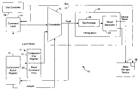
Figure 1 schematically illustrates a mass storage data protection system
10 for use with a mass storage device 11 in a gaming machine. The system
preferably
consists of a control and status register 12, a comparator command register
13, a
command latch 14, a command comparator 15, and a timing block 16. Since the
primary protection of the mass storage device in a gaming machine is to
prevent
unauthorized writing to the mass storage device, the system will be described
with
reference to protecting the mass storage device from unauthorized write
commands.
However, those skilled in the art will understand that other commands, as
desired,
may also be included for protection of the mass storage device.
Additionally, system 10 is being described herein for providing
protection for a single mass storage channel. System 10 would need to be
replicated to
protect additional channels.
CA 02312096 2000-06-22
4
In a preferred embodiment, mass storage data protection circuit 10
includes control and status register 12 that provides information regarding
the function of
the circuit. Preferably, the control and status register is an 8 bit register.
Bits 0 and 1
preferably serve as the comparator user register address pointer.
Bit ~ preferably is used to determine when a write fault that is generated
should be a non-maskable interrupt (NMI). If this bit is set high, then any
faults
generated by the data protection circuit will be an III. If faults are going
to be used to
create ~IIs, then the system must deal with any write faults. Hence, this bit
and VVIIs
are used to make the system an active one as opposed to a passive one.
Bit 6 preferably serves as the jumper. If bit 6 is high then the jumper is
removed and the data protection system is activated, i.e., it is set to write
protect. If the
bit is low then thejumper is installed and the data protection system is not
activated, i.e..
data may be written to the mass storage device.
Finally, bit 7 preferably becomes high whenever a data write is attempted
to the mass storage device and the jumper is removed. In order to clear the
bit, a 1 must
be purposefully written to the bit location.
The remaining bits may be unused or used as desired.
Comparator command register 13 includes a fixed command array 20 and
preferably includes a comparator user register 21. Fixed command array 20
includes
ANSI commands that are directed to write commands. The write commands are
preferably set by the ATA (AT attachment) device interface specification,
which
currently is the General industry standard that defines command sets.
Comparator user
register 21 is a register through which additional commands to be excluded may
be
loaded into command comparator 15. In the preferred embodiment, up to four
additional
commands may be loaded into comparator user register 21 to cause a write fault
if sent to
the mass storage device. The individual user comparator registers may be read
or written
by setting the address in the control and status register and then reading or
writing the
comparator user register access port. Generally, if the system includes a
comparator user
register, upon start-up of the mass storage data protection system, the
comparator user
register will have to be initialized in order to determine the commands
needed.
As noted above, comparator user register 21 is used to store additional
command values that must not be executed. Thus, the purpose of the comparator
user
registers is to include vender specific commands that could cause data to be
modified on
CA 02312096 2004-07-27
the mass storage device, preferred sequence of software execution includes the
software querying the mass storage device to identify itself, compare the
identification
table of valid devices, and then load the user registers with those vender
specific
commands that will cause data modification. s noted previously, up to four
additional
vender specific commands may preferably be added to the comparator command
register. Preferably, these registers are initialized to FF at reset.
Command latch 14 is connected to the bus 27 of the respective channel
that is being protected in the mass storage device. Command latch 14 stores
the data
values written by the disk controller 28 to the mass storage device command
register
29. Values that are written to the command latch are compared with values
stored in
the command comparator to determine if a write fault and device reset should
be
generated. Commands are stored in this latch only if the write enable jumper
pin is
high, i.e., the jumper is removed. If this pin is low, it signals that the
write enable
jumper is installed and that device writes are currently being allowed and
thus it is not
necessary to monitor commands.
In a preferred embodiment, mass storage device 11 is an IDE hard disk
drive and command latch 14 is an IDE command latch.
Timing block 16 of the mass storage data protection system preferably
includes a reset generator 25 and a synchronizer 26. Reset generator 25 is
responsible
for generating a reset signal to the channel on which a write fault has
occurred. If the
command comparator circuit detects a write operation is attempted, it signals
the reset
generator to send a reset pulse to the channel. Preferably, the reset
generator uses a
14.318 MHz input clock that is available in the mass storage data protection
system.
Preferably, the input clock is divided by 512 to generate a 3.8 microsecond
wide reset
pulse. Currently, the minimum specification for the reset pulse to an IDE
device is 25
microseconds. The reset generator also generates a reset to the IDE device by
logically "ORing" the system reset with the reset generator reset. This allows
the IDE
device to be reset at power up or power down. Synchronizer 26 is provided for
synchronizing between asynchronous and synchronous signals provided from
comparator 1 S and provided to reset generator 25. Those skilled in the art
will
understand that other arrangements or circuits maybe used for timing block 16,
such
as for example logic circuits.
CA 02312096 2000-06-22
6
The command comparator, as noted above, compares the values written to
the command latch with values stored in the comparator command register. If a
successful comparison takes place, a signal is sent to the device reset
generator to cause a
device reset to occur. Additionally, the comparator sets the write fault bit 7
in the control
and status register high.
Figure 2 illustrates a gaming machine 30 that includes a housing 31, at
least one user input 32 coupled to the housing, a display 33, such as, for
example, a CRT,
LCD or plasma display, coupled to the housing, a money input 34 and a money
output 3~.
The gaming machine includes a control system 36 that includes a data mass
storage
device 11 and the mass storage data protection system 10 in accordance with
the present
invention.
Although the invention has been described with reference to specific
e~cemplary embodiments, it will be appreciated that it is intended to cover
all
modifications and equivalents within the scope of the appended claims.