Note: Descriptions are shown in the official language in which they were submitted.
CA 02312486 2000-OS-31
S Specification
Electromagnetic Relay
The invention relates to an electromagnetic relay having
the ability to withstand short-circuit and overload.
Conventional solutions for ensuring short-circuiting and
overload strength for a relay predominantly make use of
protective means interrupting the load current in case
of disturbances, using thermal effects. This includes in
particular fuses or bimetal contact springs.
SU 142 74 72 A1 discloses a short-circuit protection for
a rotary current motor, which is realized with the aid
of reed relays. However, the reed relays are disposed
separately from the motor relays there. In particular,
with respect to the motor relays which switch on the
voltage supply of the motor, there is no enquiry possi-
ble as to an overload or short circuit state.
It is the object of the invention to provide an inexpen-
sive, integrated and in particular space-saving solution
for a short-circuit- and overload-proof relay, in which
in particular a differentiated response of the protec-
tive means in case of permanent overload of the relay,
and not only in case of short-time current peaks, is
desired.
According to the invention, this object is met by an
electromagnetic relay comprising
- a magnetic system containing an exciting coil
through which a control current flows, a core and an
CA 02312486 2000-OS-31
-2-
armature, with the core and the armature forming at
least one operating air gap,
- at least one movable contact element and at least
one fixed contact element through which one load
current circuit each can be closed,
- coil and contact terminal elements,
- a reed contact in each load current circuit, which
is coupled to a load current conductor having a load
current flowing therethrough, and
- means for generating and processing an overcurrent
signal and for switching off the control current.
A relay according to the invention is adapted to be re-
set to a normal operating state by interruption of the
control current. In comparison with Hall sensors, which
are also suitable for detecting a magnetic field emanat-
ing from a raised load current, reed contacts offer the
advantages of a temperature-independent behavior, simple
adjustment of triggering threshold values and simple
realization of evaluation circuits.
Preferred developments concerning the arrangement of the
reed contact in relation to the load current conductor,
the shielding of the reed contact from the magnetic
field of the exciting coil and with respect to the means
for generating and processing the overcurrent signal and
for switching off the control current are indicated in
the dependent claims. .
The invention shall now be elucidated in more detail by
way of embodiments shown in the drawings, wherein
Fig. 1 shows a relay according to the invention, com
prising a reed contact pre-assembled to a cir
cuit board;
CA 02312486 2000-OS-31
-3-
Fig. 2 shows the reed current pre-assembled to a cir-
cuit board, along with a coupled load current
conductor according to Fig. 1;
Fig. 3 shows a modification of a relay according to the
invention comprising a reed contact inserted
into a header;
Fig. 4 shows the reed contact inserted in a header
along with a coupled load current conductor ac-
cording to Fig. 3;
Fig. 5 shows a further modification of a relay accord-
ing to the invention along with a reed contact
pre-assembled to a header;
Fig. 6 shows the reed contact pre-assembled to the
header along with a coupled load current conduc-
tor according to Fig. 5;
Fig. 7 shows a basic circuit diagram of a relay accord-
ing to the invention, comprising an auxiliary
reed contact and an auxiliary winding as over-
current protection elements;
Fig. 8 shows a basic circuit diagram of an embodiment
comprising an auxiliary relay as overcurrent
protection element; .
Fig. 9 shows a basic circuit diagram of a further em-
bodiment comprising a positive temperature coef-
ficient resistor and a protective resistor as
overcurrent protection elements;
CA 02312486 2000-OS-31
-4-
Fig. 10 shows a basic circuit diagram of a bistable em-
bodiment comprising a capacitor as pulse con-
trolling element;
Fig. 11 shows a basic circuit diagram of an embodiment
comprising an electronic evaluation unit for
overcurrent recognition and load current deacti-
vation; and
Fig. 12 shows a realization of the electronic evaluation
unit according to Fig. 11.
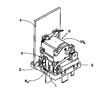
Figs. 1 to 6 show various embodiments of a relay accord-
ing to the invention, comprising different modes of cou-
pling a reed contact KR to a load current conductor 1. In
the embodiment of Fig. 1, reed contact KR is pre-assem-
bled to a circuit board 4. A header 5 has a magnetic
system 6 arranged thereon, comprising a core, an arma-
ture and an exciting coil WR. The axis of exciting coil
WR extends parallel to the base plane of header 6. In an
outer portion on header 5, circuit board 4 is attached
in upright manner, perpendicularly to the base plane of
header 5. The reed contact KR has two sheet-metal termi-
nal plates 2 and 3 connected thereto (cf. also Fig. 2) .
By suitable choice of the distance between the two
sheet-metal terminal plates 2 and 3, it is possible to
define switching thresholds for the reed contact KR. The
two sheet-metal conductor terminating plates 2 and 3 are
provided, along with reed contact KR, on a circuit board
4, with reed contact KR being oriented perpendicularly to
the base plane of header 5. In accordance with a pre-
ferred embodiment, reed contact KR thus is disposed per-
pendicularly to the axis of exciting coil WR, so that
reed contact KR is insensitive with respect to the mag-
netic stray flux of exciting coil WR. Load current con-
ductor 1 has a portion arranged perpendicularly to reed
CA 02312486 2000-OS-31
-5-
contact KR, and in this respect it is to be ensured by
suitable conductor design that the magnetic field gener-
ated by load current conductor 1 penetrates reed contact
KR in central and parallel manner. With this embodiment,
this is achieved in that the respective portion of load
current conductor 1 is constituted by a sheet-metal
strip having its sheet-metal plane extending parallel to
reed contact KR .
In the embodiment shown in Fig. 3, magnetic system 6 is
arranged on header 5 such that the axis of exciting coil
WR extends parallel to the base plane of header 5. Be-
tween magnetic system 6 and header 5, reed contact KR is
mounted perpendicularly to the axis of exciting coil WR
and parallel to the base plane of header 5. In this em-
bodiment, too, reed contact KR is connected to two sheet-
metal contacting members 2 and 3 (cf. also Fig. 4). The
two sheet-metal contacting members 2 and 3 are spaced
apart by a distance determining the switching threshold
of reed contact KR. The unit constituted by sheet-metal
contacting members 2 and 3 and reed contact KR is insert-
ed in the header 5, with the load current conductor 1
having a portion inserted centrally through a sensor
ring RS constituted by reed contact KR and sheet-metal
contacting members 2 and 3. Load current conductor 1 in
this portion is formed by a cranked sheet-metal strip so
that sensor ring RS, at a free end of the sheet-metal
strip, is arranged perpendicularly~to load current con-
ductor 1 and encloses the same. As an alternative to the
embodiment shown in Fig. 4, sensor ring RS may also be
constituted by a U-shaped magnetically conducting flux
ring and a reed contact KR coupled thereto via two air
gaps.
Fig. 5 shows an embodiment of a relay comprising a reed
contact KR pre-assembled to a header 5, with reed contact
CA 02312486 2000-OS-31
-6-
KR being oriented perpendicularly to the base plane of
header 5. In this embodiment, magnetic system 6 is
mounted on header 5 in such a manner that the axis of
exciting coil WR extends parallel to the base plane of
header 5. Load current conductor 1 is constituted in
essence by a sheet-metal strip, with a first end of load
current conductor 1 being passed perpendicularly through
the header and serving as terminal element. The second
end of load current conductor 1 extends parallel to the
axis of exciting coil WR (cf. also Fig. 6). Load current
conductor 1, in a central portion thereof, is formed
into a loop enclosing reed contact KR. By forming load
current conductor 1 in corresponding manner in this cen-
tral portion, it is ensured that the magnetic field cou-
pled by load current conductor 1 into reed contact KR
penetrates the reed contact KR in central and parallel
manner. Reed contact KR, together with its terminal
wires, is bent in U-shaped manner and has the ends of
the terminal wires attached to extensions of two termi-
nal loops 7 and 8. The connection of reed contact KR to
the extensions of the terminal loops 7 and 8 disposed
below magnetic system 6 can be established, for example,
by soldering or resistance welding. The distance between
the two terminal loops 7 and 6 defines the switching
threshold of reed contact KR. In all of the embodiments
shown in Figs. 1 to 6, an advantage consists in that
mounting of the reed contact KR and coupling of the reed
contact KR to load current conductor. 1 do not require any
significant constructional changes to the relay.
Fig. 7 shows a basic circuit diagram of a relay compris-
ing an auxiliary reed contact and an auxiliary winding
as overcurrent protection elements. Relay R comprises a
control current circuit having an exciting coil WR asso-
ciated therewith through which a control current IS
flows, and it comprises a load current circuit, with the
CA 02312486 2000-OS-31
load current IL being controllable by a movable contact
element KB and a stationary or fixed contact element KF
of relay R. Arranged in the control current circuit is a
reed contact KR by means of which the control current IS
through exciting coil WR can be controlled. Reed contact
KR is coupled to a load current conductor having the load
current IL flowing therethrough. The magnetic coupling
between the load current conductor and the reed contact
KR is indicated in symbolic manner hereinafter by a load
current conductor winding WL. In the embodiment accord-
ing to Fig. 7, reed contact KR has one movable contact
element El and two fixed contact elements E2 and E3.
Moreover, an auxiliary winding WH1 is coupled to reed
contact KR in such a manner that, in an overcurrent state
of operation, a magnetic field emanates from auxiliary
winding WH1 that has the same direction as a magnetic
field caused by a load current conductor winding WL.
Load current IL is switched directly via movable contact
element KB and fixed contact element KF of relay R. Reed
contact KR may be disposed axially inside load current
conductor winding WL. A reed contact KR disposed outside
load current conductor winding WL and arranged parallel
to the winding axis is possible as well. An alternative
to coupling the reed contact KR to a load current conduc-
tor winding WL is an arrangement of reed contact KR in-
side a loop-shaped section of a load current conductor.
To prevent that the magnetic field of exciting coil WR of
relay R takes influence on the reed contact KR, reed con-
tact KR advantageously is to be arranged perpendicularly
to the axis of exciting coil WR. As an alternative there-
to, said influence can be prevented by a magnetically
conductive sheet-metal shielding plate between exciting
coil WR and reed contact KR. By means of the shielding
plate, a magnetic stray field caused by exciting coil WR
CA 02312486 2000-OS-31
_g_
is short-circuited. Another possibility consists in in-
troducing the magnetic stray flux emanating from excit-
ing coil WR purposefully into reed contact KR. This is
possible, for example, by regulating the control current
IS. By doing so, reed contact KR is subjected to the ef-
fect of a constant magnetic flux as offset. By defini-
tion of corresponding threshold values at reed contact
KR, it is thus possible to utilize the magnetic stray
field.
In a normal state of operation, reed contact KR connects
exciting coil WR of relay R to a control voltage source
US via a f first f fixed contact element E2 of reed contact
KR. In this state, the auxiliary winding WH coupled to
the second fixed contact element E3 is separated from
the movable contact element E1 of reed contact KR and
thus from control voltage source US. In contrast thereto,
in an overcurrent state of operation, the movable con-
tact element E1 of reed contact KR is connected to the
second fixed contact element E3 and disconnected from
the first fixed contact element E2. Due to this, excit-
ing winding WR of relay R is separated from control volt-
age source US, whereas auxiliary winding WH is connected
to control voltage source US. The connection between mov-
able contact element E1 of reed contact KR and the second
fixed contact element E3 is maintained also after inter-
ruption of the load current circuit, due to the magnetic
flux emanating from auxiliary winding WH. Only after sep-
aration from control voltage source US will relay R re-
turn to the normal state of operation.
Fig. 8 shows a basic circuit diagram of an alternative
possible development of a short-circuit-proof relay in
which the overcurrent protection function is realized by
means of an auxiliary relay RH1. Auxiliary relay RH1 com-
prises a movable contact element E4 and two fixed con-
CA 02312486 2000-OS-31
-9-
tact elements E5 and E6, with the movable contact ele-
ment E4 being connected to the first fixed contact ele-
ment E5 in the normal state of operation. Movable con-
tact element E4 is connected directly to a control volt-
s age input terminal so that the control voltage US is ap-
plied directly to exciting coil WR of relay R. Reed con-
tact KR is connected between the contact element E4 of
auxiliary relay RH1 and the second fixed contact element
E6.
Coil WHZ of auxiliary relay RH1 is currentless in the nor-
mal state of operation. In the overcurrent state of op-
eration, reed contact KR is closed whereby control
voltage US is applied directly to coil WHZ of auxiliary
relay RH1. As a consequence thereof, movable contact ele-
ment E4 is connected to the second fixed contact element
E6 of auxiliary relay RHl and separated from the first
fixed contact element E5. As a result hereof, exciting
coil WR of relay R is currentless in the overcurrent
state of operation. Due to the fact that the load cur-
rent circuit and the control current circuit of auxilia-
ry relay RH1 are connected in series in the overcurrent
state of operation, auxiliary relay RH1 maintains its
switching state also after interruption of the load cur-
rent circuit of relay R by actuation of contact element
KH and associated opening of reed contact KR. If a time
delay unit is arranged in addition between reed contact
KR and second fixed contact element E6 of auxiliary relay
RH1, short-time load current peaks do not result in a re-
sponse of the overcurrent protection means. Instead of
auxiliary relay RH1, it is also possible to use a second
reed contact which then is coupled to an associated aux-
iliary winding.
Fig. 9 shows an additional alternative for realizing an
overcurrent protection, comprising a positive tempera-
CA 02312486 2000-OS-31
- 10-
ture coefficient resistor RpT~ and a protective resistor
R" connected in series therewith. These two overcurrent
protection elements are connected to control voltage
source US in series with reed contact KR, with the reed
contact KR being first closed in the overcurrent state of
operation and being opened in the normal state of opera-
tion. Exciting coil WR of relay R is connected in paral-
lel with reed contact KR and protective resistor R~ and
in series with positive temperature coefficient resistor
R~~. Due to the fact that protective resistor R", in com-
parison with the internal resistance of exciting coil WR
of relay R, is of low resistance, an increased current
flows through positive temperature coefficient resistor
RpTC upon closure of reed contact KR, whereby positive
temperature coefficient resistor Rpr~ is heated and chang-
es to high resistance. Due to this, the voltage drop at
exciting coil WR of the relay decreases, so that inter-
ruption of the load current circuit takes place. Depend-
ing on the heating behavior of positive temperature co-
efficient resistor Rp.r~, a time delay is achieved, whereby
short-time load current peaks do not effect protection
triggering. In addition thereto, positive temperature
coefficient resistor RpT~ performs a state storing func-
tion provided that the residual current through exciting
coil WR of relay R is sufficient to maintain the required
temperature of the positive temperature coefficient re-
sistor. In that case, positive temperature coefficient
resistor RpZ.C remains in the high-resistance state also
after re-opening of reed contact KR. Only after separa-
tion from control voltage source US and cooling down of
positive temperature coefficient resistor RPT~ will re-
newed driving of relay R be possible.
Fig. 10 shows a basic circuit diagram of an embodiment
comprising a bistable relay RZS and a capacitor CS. Bi-
stable relay RZS is provided with a first exciting coil
CA 02312486 2000-OS-31
-11-
WRl and a second exciting coil WRZ. First exciting coil WRl
of relay Rzs is connected to control voltage source Us in
series with capacitor Cs. Second exciting coil WRZ is con-
nected to control voltage source Us in series with reed
contact KR and is of opposite winding direction as com-
pared to first exciting coil WRl. A positive pulse of
current Isl through first exciting coil WR1 thus effects
closing of the load current circuit, whereas a positive
pulse of current Isz through second exciting coil WRZ in-
terrupts the load current circuit. In case of over-
current, reed contact KR connects second exciting coil WRz
at first to control voltage source Us, whereupon relay Rzs
changes to a stable switched off state. Only after deac-
tivation and renewed switching on of control voltage Us
does the first exciting coil WR1 receive a positive cur-
rent pulse via capacitor Cs, whereby relay Rzs changes
over to a stable switched-on state.
In the basic circuit diagram of a modification of the
short-circuit- and overcurrent-proof relay, the over-
current protection functions are integrated in an over-
current protection means that is realized by an elec-
tronic circuit CCU. Electronic circuit CCU comprises
four terminals, with the control voltage Us being applied
between a first control voltage terminal K1 and a second
control voltage terminal K2. In addition thereto, elec-
tronic circuit CCU comprises a first exciting coil ter-
minal K3 and a second reed contact terminal K4. First
reed contact terminal and second exciting coil terminal
are connected to second control voltage terminal K2.
Electronic circuit CCU, as application-specific in-
tegrated circuit (ASIC), can be integrated very easily
in circuit board 4 of the relay shown in Fig. 1 or also
in header 5 of the relays shown in Figs. 3 and 5.
CA 02312486 2000-OS-31
-12-
A possible realization of the overcurrent protection
means according to Fig. 11 in terms of circuit technol-
ogy is shown in~Fig. 12. Electronic circuit CCU is seg-
mented in the form of a timing element U1, a switching-
on segment U2 for exciting coil WR, and a switching-off
segment U3. Switching-on segment U2 for relay coil WR
consists of a pnp transistor T1 connected in series with
relay coil WR between the two control voltage terminals
K1 and K2, and of a protective resistor R2. Transistor
T1 has its emitter connected to first control voltage
terminal K1 and its collector connected to first excit-
ing coil terminal K3. Protective resistor R2 of switch-
ing-on segment U2 is connected between the base of tran-
sistor T1 and the second control voltage terminal K2.
The switching-off segment U3 for exciting coil WR is con-
stituted by a first resistor R4 and a second resistor
R3. First resistor R4 is connected in parallel to excit-
ing coil WR, while second resistor R3 of switching-off
segment U3 is connected between first exciting coil ter-
minal K3 and second reed contact terminal K4.
Timing element U1 comprises a comparator CMP and an RC
member, with the capacitor C1 of the RC member having a
first terminal connected to the first control voltage
terminal K1. Resistor Rl of the RC member is connected
between second terminal K5 of capacitor C1 and second
reed contact terminal K4. The comparator CMP proper con-
sists of a pnp transistor T2 and a Zener diode D1, with
the transistor T2 of comparator CMP having its emitter
connected to first control voltage terminal K1 while the
collector of transistor T2 is connected to the base of
transistor T1 of the switching-on segment U2. The base
of transistor T2 of comparator CMP is connected to the
cathode of Zener diode D1 the anode of which is connect-
CA 02312486 2000-OS-31
-13-
ed between capacitor C1 and resistor R1 of the RC mem-
ber.
When control voltage US is applied to control voltage
terminals K1 and K2 of electronic circuit CCU, a control
current flows across the emitter-to-base path of tran-
sistor T1 of switching-on segment U2 and connects tran-
sistor T1 through. Exciting coil WR of relay R thus has a
switching voltage supplied thereto, whereupon the load
current circuit is closed. Switching of transistor T1
takes place via resistor R2, with the switching speed of
the transistor playing an important role. For, it must
be ensured prior to activation of timing element U1 that
relay R is connected through first by application of
control voltage US. In doing so, the function of timing
element U1 consists in blocking transistor T2 of compa-
rator CMP until transistor T1 of switching-on segment U2
is connected through. Thereafter, transistor T2 of com-
parator CMP also changes over to a stable blocked state,
which is achieved by the feedback of the collector volt-
age of transistor T1 via resistors R3, Rl and via Zener
diode D1.
In case of overcurrent, reed contact KR closes and con-
nects the base of transistor T2 directly to second con-
trol voltage terminal K2. This effects discharge of ca-
pacitor C1 via resistors R1 and R3. Upon exceeding the
breakdown voltage at Zener diode D~, a control current
flows through the emitter-to-base path of transistor T2
which connects transistor T2 through and electrically
connects the base of transistor T1 of switching-on seg-
ment U2 to first control voltage terminal K1. As a re-
sult of this, switching-off segment U3 is activated via
transistor T2 of timing element U1, whereby transistor
T1 of the switching-on segment U2 changes over to the
blocked state. Consequently, exciting coil WR of relay R
CA 02312486 2000-OS-31
- 14-
is disconnected from control voltage source US so that
the load current circuit is interrupted. The consequence
hereof is that reed contact KR opens again as there is no
overcurrent flowing through the load circuit then.
Switching-off segment U3 remains activated since tran
sistor T2 of comparator CMP as before is in the conduct
ing state. This operational state is maintained or
stored until control voltage US at control voltage termi
nals K1 and K2 of electronic circuit CCU is switched
off .
Undesired response of the overcurrent protection means
in case of switching-on or switching-over current peaks,
which as a rule are less than some 100 milliseconds, is
prevented by timing element U1. By suitable dimensioning
of resistor R1, capacitor Cl of timing element U1, and
of resistors R3 and R4 of switching-off segment U3 and
by selection of a Zener diode D1 with a suitable break-
down voltage, the time behavior of electronic circuit
CCU can be matched to the duration of switching-on and
switching-over current peaks to be expected, respective-
ly. At the same time, interference pulses at control
voltage terminals K1 and K2 are filtered out by means of
timing element U1 as well.