Note: Descriptions are shown in the official language in which they were submitted.
CA 02312706 2004-01-26
1
GAS DETECTION APPARATUS USING A COMBINED INFRARED
SOURCE AND HIGH TEMPERATURE BOLOMETER
FIELD OF THE INVENTION
The field of the invention is electro-optical radiation sources and detectors,
and more particularly, to an apparatus that simultaneously functions as an
electro-
optical radiation source and an electro-optical radiation detector.
BACKGROUND OF THE INVENTION
Non-dispersive Infrared (NDIR) techniques utilizing the characteristic
absorption bands of gases in the infrared have long been considered as one of
the
best methods for composite gas measurement. These techniques take advantage of
the fact that various gases exhibit substantial absorption at specific
wavelengths in
the infrared radiation spectrum. The term "non-dispersive" refers to the type
of
apparatus
CA 02312706 2000-06-05
WO 99/28729 PCT/US98/25771
2
incorporating this particular measurement technique, typically including a
narrow band pass interference filter (as opposed to a "dispersive" element,
such as a prism or a diffraction grating) to isolate and pass radiation in a
particular wavelength band from a spectrally broad band infrared source.
The gas concentration is discerned from the detected intensity modulation of
source radiation that is passed by the filter coincident in wavelength with a
strong absorption band of the gas to be measured.
A prior art NDIR gas analyzer typically includes a discrete infirared
source with a motor-driven mechanical chopper to modulate the source so
that synchronous detection may be used to discriminate spurious infrared
radiation from surroundings; a pump to push gas through a sample chamber;
a narrow band-pass interference filter; a sensitive infrared detector, and
infrared optics/windows to focus the infrared energy from the source onto
the detector. Although the NDIR gas measurement technique is recognized
as one of the most effective methodologies for composite gas measurement
available, it has not enjoyed wide application because of its complexity and
high cost of implementation.
Infrared absorption instruments traditionally contain a source of
infrared radiation, a means of spectral selection for the gas under study, an
absorption cell with associated gas sample handling and/or conditioning, any
necessary optics, a sensitive infrared detector, and associated signal
processing electronics. A typical source of infrared radiation includes an
incandescent filament or a thin film conductor. The emissions spectrum of
the infrared source may be tailored via surface texturing techniques, as are
described in U.S. Patent No. 5,838,016. The invention simplifies and
reduces the cost of an infrared instrument by integrating the function of the
infrared source and infrared detector into a single self-supporting thin-film
bolometer element. This element is packaged with inexpensive molded
plastic optics and a conventional spectral filter to make a transistor-size
"sensor engine." Combined with a simple reflector plate to define the gas
sampling region, this sensor engine provides a complete gas sensor
CA 02312706 2000-06-05
WO 99/28729 PCT/US98/25771
3
instrument which is extremely inexpensive and which will approach the
sensitivity of conventional infrared absorption instruirnents.
SUMMARY OF THE INVENTION
The present invention is an apparatus for detecting a gas having a
distinct infrared radiation absorption characteristics. The apparatus includes
a spectral source/bolometer for conducting an electrical current and for
producing an infrared radiation. The source/bolometer is disposed along an
axis and has a temperature and a characteristic resistance; the characteristic
resistance is a predetermined function of the temperature. The apparatus
further includes a concentrating reflector for directing the infrared
radiation
along the axis, first through a spectral filter and then through the gas. The
apparatus also includes a return reflector disposed along the axis beyond the
spectral filter and the gas, such that at least a portion of the infrared
radiation
passing through the filter and the gas is reflected back through the gas and
the filter to the source/bolometer. The apparatus further includes a
driver/detector for driving a current through the source/bolometer, for
determining the characteristic resistance, and for detecting the gas from a
variation of the characteristic resistance.
In one embodiment, the source/bolometer includes a thin-film
conductor.
In another embodiment, the source/bolometer includes a filament
conductor.
In another embodiment, the sourcelbolometer includes surface
texturing so as to tailor a spectral characteristic of the infrared radiation.
In a further embodiment, the concentrating reflector is disposed about
the axis so as to form a first aperture along the axis and a second aperture
along the axis, the source/bolometer is disposed at the first aperture and the
spectral filter is disposed at the second aperture.
In another embodiment, the concentrating reflector forms a compound
parabolic concentrator.
CA 02312706 2007-10-23
4
In another embodiment, the return reflector defines a gas sampling
region.
In another embodiment, the return reflector includes a flat reflective
surface disposed substantially perpendicular to the is.
In another embodiment, the return reflector includes a contoured
reflective surface disposed substantially about the axis.
In one embodiment, the contoured reflective surface includes a
parabolic surface.
In another embodiment, the spectral filter substantially passes infrared
radiation within a first passband and substantially blocks infrared radiation
outside of the first passband.
In a further embodiment, the spectral filter includes a micromesh
reflective filter.
In another embodiment, the micromesh reflective filter is fabricated
using micro-electro-mechanical systems technology.
In yet another embodiment, the driver/detector includes a Wheatstone
bridge circuit having a first resistor pair and a second resistor pair,
wherein a
first resistor of the first resistor pair includes the source/bolometer.
In another embodiment, a second resistor of the first resistor pair
includes a blind source/bolometer being identical to the source/bolometer and
filtered at a second passband.
In another embodiment, a ratio of the first resistor pair is substantially
equal to a ratio of the second resistor pair.
Accordingly, in one aspect the invention resides in a method of
detecting a gas having a distinct infrared radiation absorption
characteristics,
comprising conducting an electrical current through a spectral
source/bolometer and thereby producing an infrared radiation, said source
bolometer being disposed along an axis and having a temperature and a
characteristic resistance, said characteristic resistance being a
predetermined
function of said temperature; directing said infrared radiation along said
axis,
first through a spectral filter and then through said gas; reflecting at least
a
portion of said infrared radiation passing through said filter and said gas
back
through said gas and said filter to said source/bolometer; and, driving a
current through said source/bolometer, determining said characteristic
CA 02312706 2007-10-23
4a
resistance, and detecting said gas from a variation of said characteristic
resistance.
In another aspect, the invention resides in an apparatus for detecting a gas
having distinct infrared radiation absorption characteristics, comprising a
spectral
source/bolometer for conducting an electrical current and for producing an
infrared
radiation, said source/bolometer being disposed along an axis and having a
temperature and a characteristic resistance, said characteristic resistance
being a
predetermined function of said temperature; a return reflector disposed along
said
axis beyond said gas, such that at least a portion of said infrared radiation
passing
through said gas is reflected back through said gas to said source/bolometer;
and a
driver/detector for driving a current through said source/bolometer, for
determining
said characteristic resistance, and for detecting said gas from a variation of
said
characteristic resistance.
BRIEF DESCRIPTION OF THE DRAWINGS
The foregoing and other objects of this invention, the various features
thereof, as well as the invention itself, may be more fully understood from
the
following description, when read together with the accompanying drawings in
which:
FIG. 1 illustrates one preferred embodiment of a combined infrared
source and sensor;
CA 02312706 2000-06-05
WO 99/28729 PCT/US98/25771
FIG. 2 illustrates another embodiment of the combined infrared source
and sensor shown in FIG. 1;
FIG. 3 illustrates a Wheatstone bridge used to drive the
source/bolometer component of the source and sensor shown in FIG. 1; and,
5 FIG. 4 shows a test configuration that incorporates the Wheatstone
bridge of FIG. 3.
DETAILED DESCRIPTION OF THE PREFERRED EMBODIMENT
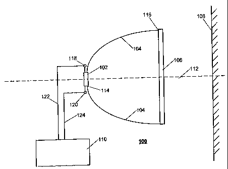
Referring now to the drawings, FIG. 1 illustrates one preferred
embodiment of a combined infrared source and sensor 100 including a
spectral source/bolometer 102, a concentrating reflector 104, a spectral
filter
106, a return reflector 108 and a driver/detector circuit 110. The
concentrating reflector 104 is disposed substantially symmetrically about an
axis 112 so as to form a first aperture 114 and a second aperture 116. The
source/bolometer 102 is disposed along the axis 112 at the first aperture 114
so as to direct the infrared radiation from the source/bolometer 102 along an
axis 112 toward the second aperture 116. The return reflector 108 is
disposed along the axis 112 such that the infrared radiation from the
source/bolometer 102 directed along the axis 112 is reflected back along the
axis 112 through the second aperture 116 toward the source/bolometer 102.
The spectral filter 106 is disposed along the axis 112 at the second aperture
116. Infrared radiation passing through the second aperture 116 (either from
the source/bolometer 102 to the return reflector 108, or vice versa) passes
through and may be modified by the spectral filter 106. The driver/detector
circuit 110 is electrically coupled to a first terniinal 118 and a second
terminal 120 of the source/bolometer 102 via a first electrical conductor 122
and a second electrical conductor 124, respectively.
The spectral source/bolometer 102 may include a filament, a thin-film
element or other infrared radiating components known to those in the art.
The first terminal 118 and the second terminal 120 are electrically coupled to
the source/bolometer 102 such that an external driver (e.g., the
CA 02312706 2000-06-05
WO 99/28729 PCT/US98/25771
6
driver/detector circuit 110) can apply a voltage across the source/bolometer
102 via the first terminal 120 and the second terminal 122, thereby inducing
current flow through the source/bolometer. In one preferred embodiment,
the surface of the source/bolometer may be textured so as to selectively
tailor the infrared emissions spectrum to substantially match the absorption
characteristics of the target gas to be detected.
In the illustrated embodiment of the invention, the concentrating
reflector 104 includes a parabolic reflector, although other reflector shapes
(e.g., spherical, conical and custom contoured) may be used to adequately
direct the infrared radiation from the source/bolometer 102 along the axis
112. Similarly, although the embodiment illustrated in FIG. 1 includes a flat
reflector, other reflector shapes may be use. The spectral filter 106 may
include any one of several conventional designs known to those in the art to
achieve tight spectral control of the infrared emission. In general, the
spectral filter 106 passes only infrared radiation that is within a
predetermined passband. The predetermined passband is chosen as a
function of the target gas to be detected.
The electrical resistance R of the source/bolometer 102 varies as a
function of its equilibrium temperature T, i.e., R = f{T}. The function f{T}
may be determined empirically or analytically for a particular
sourceJbolometer 102. For a given amount of input power applied to the
source/bolometer 102, the equilibrium temperature T of the
source/bolometer 102 is dependent upon how fast it cools, and the cooling
rate of the source/bolometer 102 is dependent on the optical absorption
characteristics of its immediate environment. In general, different gases are
known to each exhibit distinct optical absorption characteristics. The
spectral filter 106 may be selected such that the infrared source and sensor
100 forms a tuned cavity band emitter corresponding to the absorption
characteristics of the gas under study. Thus, the gas may be detected in the
presence of the source/bolometer 102 by monitoring the resistance R of the
source/bolometer 102.
CA 02312706 2000-06-05
WO 99/28729 PCT/US98/25771
7
FIG. 2 illustrates another embodiment of the present invention, that
forms an infrared gas monitoring component 200 of an integrated on-board
exhaust NOx meter (where x is a positive non-zero integer). This
embodiment utilizes silicon micro-machining technology to construct a
sensor that is radically simpler than conventional infrared absorption
instruments. This embodiment simplifies and reduces the cost of an infrared
absorption instrument by integrating the function of the infrared source and
infrared detector into a single self-supporting thin-film source/bolometer
102. The source/bolometer 102 includes inexpensive molded plastic optics
and a conventional spectral filter 106 to make a transistor-size sensor engine
202. Combined with a simple reflector plate to define the gas sampling
region, this sensor engine provides a complete gas sensor instrument which
is extremely inexpensive and which will approach the sensitivity of
conventional infrared absorption instruments.
The embodiment of FIG. 2 illustrates a novel, low-cost infrared gas
sensor using a thin-film sowce/bolometer 102 in an open path atmospheric
gas measurement. As described herein, the source/bolometer 102 reaches
radiative equilibrium with its surroundings at a slightly lower temperature if
gas absorption frustrates light re-imaging source/bolometer 102. The
concentrating reflector 104, in this case a compound parabolic concentrator,
defines a relatively narrow illumination cone (+/- 15 degrees about the axis
118) and the passive return reflector 108 is contoured to provide a pupil-
image of the spectral filter 106 onto itself. The entire sensor engine 202 can
be mounted in a substantially small package, e.g., on a TO-8 transistor
header.
Tight spectral control of the infrared emission is important in making
the source/bolometer 102 work well. The device is particularly effective if
the amount of radiation absorbed by gas molecules under study is
measurably large in terms of the overall thermal budget of the bolometer
surface. Thus, a tuned cavity band emitter is preferably constructed with
spectral resolution (dl/l) around 0.1, roughly the performance achieved to
date
CA 02312706 2000-06-05
WO 99/28729 PCT/US98/25771
8
with micromesh reflective filters. This increases the conversion efficiency to
nearly 15% for the NOx application. This level of surface topology (and
therefore spectral) control, is achieved through micro-electro-mechanical
systems (MEMS) technologies. An individual emitter die is packaged, together
with individual infiared detector pixel elements and thin film interference
filter
windows in TO-8 transistor cans using standard process equipment.
The embodiment illustrated in FIG. 2 uses drive and readout schemes
having a microprocessor controlled, temperature-stabilized driver to determine
resistance from drive current and drive voltage readings. The current and
voltage information shows that incidental resistances (temperature
coefficients in
leads and packages and shunt resistors, for instance) do not overwhelm the
small
resistance changes used as a measurement parameter. The Wheatstone bridge
300 shown in FIG. 3, a straightforward analog control circuit, is used to
drive the
source/bolometer 102 and detennine the incremental resistance values. The
Wheatstone bridge is simple and accurate, is substantially insensitive to
power
supply variations and is relatively insensitive to temperature. The circuit is
"resistor" programmable, but depends for stability on matching the ratio of
resistors. In one form of the invention, an adjacent "blind" pixel, i.e., an
identical bolometer element (a blind source/bolometer), filtered at some
different
waveband, is used as the resistor in the other leg of the bridge, allowing
compensation for instcument and component temperatures and providing only a
difference signal related to infiared absorption in the gas. The Wheatstone
bridge provides a simple computer interface, and since it is implemented with
relatively robust analog parts, it is not susceptible to radiation damage at
high
altitudes or in space. For the Wheatstone bridge 300 shown in FIG. 3, bridge
is
balanced when the ratio of the resistor pair RI and R2 is substantially equal
to
the ratio of the resistor pair R3 and R4 (i.e., R1/R2 = R3/R4), and to first
order,
temperature coefficients of Rl and R2 can be neglected if resistors are
matched.
The temperature coefficient of R3 is important but should have negligible
effect
across the relatively small change in temperature of the bolometer caused by
the
gas absorption. Preferably, the resistors are chosen so that the bridge is
CA 02312706 2000-06-05
WO 99/28729 PCT/US98/25771
9
substantially balanced at the target operating temperature. The estiniated
errors
from an analog readout of this circuit come from the amplifier input offset
and
input bias currents which introduce offset voltage or error term. FIG. 4 shows
a
test configuration that incorporates the Wheatstone bridge 300. Note that the
component reference designations FIG. 4 do not correspond to those in FIG. 3.
An optics test bed has been used to evaluate different configurations and
perfonn measurements of this embodiment. In an elevated ambient temperature
environment (e.g., automotive), the device is operated as instrumented tube
furnaces and to calibrate the infrared readings against a conventional gas
analyzer.
The invention may be embodied in other specific fonns without departing
from the spirit or essential characteristics thereof. The present embodiments
are
therefore to be considered in respects as illustrative and not restrictive,
the scope
of the invention being indicated by the appended claims rather than by the
foregoing description, and all changes which come within the meaning and
range of the equivalency of the claims are therefore intended to be embraced
therein.