Note: Descriptions are shown in the official language in which they were submitted.
CA 02313034 2000-06-02
TITLE OF THE INVENTION
OPTICAL AMPLIFIER
BACKGROUND OF THE INVENTION
Field of the Invention
The present invention relates to an optical amplifier mainly used in an
optical communication system and suitable for amplifying a wavelength-division
multiplexed optical signal having a band of I .5 ,u m.
Related Background Art
In optical fiber communication systems, rare earth doped optical fiber
amplifiers (referred to merely as "optical amplifiers" hereinafter) have
remarkably been developed. Particularly, a D-WDM system in which a wide
amplifying band of the optical amplifier is utilized and a communication
capacity is increased by using wavelength-division multiplexed optical signals
obtained by multiplexing a plurality of optical signals in the amplifying band
has mainly been progressed. However, although the optical amplifier has the
wide amplifying band, an amplifying property thereof has wavelength
dependency, input intensity dependency and temperature dependency.
Thus, when the wavelength-division multiplexed optical signals are
amplified collectively, there arises a problem regarding difference in gain
between the respective different optical signal wavelengths (referred to as
"channels" hereinafter). That is to say, in the D-WDM system, when the
optical amplifiers are connected in a mufti-stage fashion, the gain
differences
between the channels are accumulated, thereby causing great output signal
intensity difference ultimately. Since the transmission property of the entire
optical transmitting system is limited by a channel having minimum output
signal intensity, even when there are channels having greater output signal
intensity, the transmission property of the entire optical transmitting system
will
i
CA 02313034 2000-06-02
be reduced.
To solve this problem, various techniques have been developed. As
one of these techniques, there is means for controlling a temperature of the
entire rare earth doped optical fibers to keep the temperature constant in
order to
eliminate the temperature dependency. However, the means for controlling the
temperature of the rare earth doped optical fibers increases power consumption
and makes the entire system bulky, and, increase in the used temperature range
results in additional increase in power consumption.
Further, there is gain constant control means for keeping the gain
constant by adjusting output intensity in accordance with input intensity
after
gain spectrum is flattened by inserting a correction filter into an optical
amplifier portion in order to eliminate the wavelength dependency from the
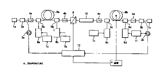
amplifying property. Fig. 44 shows an example of an optical amplifier
utilizing such means. In the optical amplifier shown in Fig. 44, optical fiber
amplifiers are connected in a two-stage fashion. The optical amplifier
comprises an input optical connector la, an output optical connector lb,
optical
couplers or beam sputters 2a, 2b, 2c, 2d, optical monitors PD 3a, 3b, 3c, 3d,
optical isolators 4a, 4b, 4c, 4d, pumping light/optical signal wavelength-
division multiplexers Sa, Sb, Sc, pumping light sources 6a, 6b, 6c, rare earth
doped optical fibers (optical fiber amplifiers) 7a, 7b, an optical variable
attenuator 8, and optical signal gain constant pumping light source control
circuits 9a, 9b. In this optical amplifier, a part of input optical signal
outputted from the input optical connector 1 a is picked up by the beam
splitter
2a and light intensity thereof is measured by the optical monitor PD 3a. The
optical signal passes through the optical isolator 4a and is incident on the
optical fiber amplifier 7a which is now maintained in a pumping condition by
the
pumping light source 6a. In this optical fiber amplifier, the optical signal
is
subjected to optical amplification by stimulated emission. The optical-
amplified optical signal passes through the optical isolator 4b, and a part of
the
2
CA 02313034 2000-06-02
light is picked up by the beam sputter 2b and light intensity thereof is
measured
by the optical monitor PD 3b. The pumping light source 6a is adjusted by the
optical signal gain constant pumping light source control circuit (AGC) 9a so
that a ratio between the input optical signal of the optical monitor PD 3a and
the
output optical signal of the optical monitor PD 3b becomes a constant value.
The optical signal passed through the first stage passes through the optical
variable attenuator 8 and is incident on the second stage. The second stage is
operated in the similar manner to the first stage, so that the signals of the
optical
monitors PD 3c, 3d are compared by the optical signal gain constant pumping
light source control circuit (AGC) 9b, and the pumping light sources 6b, 6c
are
controlled so that a ratio therebetween becomes a constant value. As a result,
even if the light intensity of the input signal is changed, gain spectrums of
the
optical fiber amplifiers in the first and second stages are kept constant.
However, in the optical amplifier utilizing the gain constant control
means as shown in Fig. 44, since the intensity of the pumping light is varied
with the light intensity of the input signal, in a small input optical signal
area
within the operation input optical signal intensity range, the intensity of
the
pumping light becomes small, thereby deteriorating noise figure. Further,
since the intensity of the pumping light is greatly changed, the first stage
of the
gain constant control requires forward pumping or bi-directional pumping.
In consideration of the above, an object of the present invention is to
provide an optical amplifier of multi-stage type having a plurality of rare
earth
doped optical fibers and in which temperature dependency of gain spectrum can
be compensated so as to be operated with constant gain spectrum regardless of
used temperature. Another object of the present invention is to provide an
optical amplifier which can be operated with constant gain spectrum regardless
of intensity of input optical signal, insertion loss of parts between stages
and
light intensity of output optical signal. A further object of the present
invention is to provide an optical amplifier in which noise figure is improved
in
3
CA 02313034 2000-06-02
a small optical signal area within an operation input optical signal range,
and a
gain configuration is kept constant regardless of intensity of input optical
signal, and output variable control can be performed.
SUMMARY OF THE INVENTION
According to a first aspect of the present invention, there is provided
an optical amplifier having a plurality of rare earth doped optical fibers in
a
mufti-stage and comprising one or more optical variable attenuator means, and
an attenuation amount control means for changing an optical attenuation amount
of the optical variable attenuator means on the basis of temperature of the
rare
earth doped optical fibers or an environmental temperature.
According to a second aspect of the present invention, there is
provided an optical amplifier having a plurality of rare earth doped optical
fibers in a mufti-stage and comprising, a replaceable optical part between the
rare earth doped optical fibers, one or more optical variable attenuator
means,
and an attenuation amount control means for changing an optical attenuation
amount of the optical variable attenuator means on the basis of temperature of
the rare earth doped optical fibers or an environmental temperature.
According to a third aspect of the present invention, in the optical
amplifier according to the first or second aspect, the attenuation amount
control
means has an optical attenuation amount table associated with the temperature,
and the optical attenuation amount of the optical variable attenuator means is
changed on the basis of the optical attenuation amount table.
According to a fourth aspect of the present invention, in the optical
amplifier according to the third aspect, when an equation obtained by applying
the regression line based on the method of least squares to the optical
attenuation amount table is represented by "optical attenuation amount -
coefficient A [dB/°C ] X temperature [°C ] + any coefficient",
the coefficient A is
selected to be within a range from -0.16 [dB/°C] to + 0.26
[dB/°C].
a
CA 02313034 2000-06-02
According to a fifth aspect of the present invention, in the optical
amplifier according to the third aspect, a wavelength band of optical signal
inputted to the optical amplifier is 1580 to 1590 nm, and, when an equation
obtained by applying the regression line based on the method of least squares
to
the optical attenuation amount table is represented by "optical attenuation
amount = coefficient A [dB/°C ] X temperature [°C ] + any
coefficient", the
coefficient A is selected to be within a range from -0.16 [dB/°C ] to -
0.04
[dB/°C ].
According to a sixth aspect of the present invention, in the optical
amplifier according to any one of first to fifth aspects, the attenuation
amount
control means changes the optical attenuation amount of the optical variable
attenuator means by using one or plural or all of intensity of input optical
signal
to the optical amplifier, an insertion loss amount of the replaceable optical
part
and intensity of output light from the optical amplifier, as well as the
temperature.
According to a seventh aspect of the present invention, there is
provided an optical amplifier having a plurality of rare earth doped optical
fibers in a mufti-stage and comprising one or more externally controllable
optical variable attenuator means, and an optical attenuation amount of the
optical variable attenuator means is varied with intensity of input optical
signal
to the optical amplifier and intensity of output light from the optical
amplifier.
According to an eighth aspect of the present invention, in the optical
amplifier according to the seventh aspect, an optical fiber amplifier in a
first
stage is subjected to pumping light intensity constant control or pumping
current
constant control, and optical fiber amplifiers in stages other than the first
and
last stages are subjected to any control other than gain constant control, and
gain spectrum of the entire optical amplifier is made constant by controlling
an
optical fiber amplifier in the last stage and the optical variable attenuator
means
between the optical fiber amplifier stages.
CA 02313034 2000-06-02
According to a ninth aspect of the present invention, in the optical
amplifier according to the seventh or eighth aspect, it comprises an optical
attenuation amount table associated with the intensity of input optical signal
to
the optical amplifier and the intensity of output optical signal from the
optical
amplifier, and the optical attenuation amount is changed in accordance with
the
table.
According to a tenth aspect of the present invention, in the optical
amplifier according to the ninth aspect, a relationship between the intensity
of
input optical signal to the optical amplifier, intensity of output optical
signal
from the optical amplifier and optical attenuation amount of the optical
variable
attenuator means is represented by "optical attenuation amount = coefficient A
X (intensity of output optical signal from the optical amplifier - intensity
of
input optical signal to the optical amplifier) [dB] + any coefficient", and
the
coefficient A has a value within a range from - 0.8 [dB/dB] to - 1.1 [dB/dB].
In the optical amplifier according to the present invention, the rare
earth doped optical fibers in the last stage may be subjected to output
constant
control.
In the optical amplifier according to the present invention, the rare
earth doped optical fibers in the first stage may be subjected to pumping
light
output constant control.
In the optical amplifier according to the present invention, the
attenuation amount control means may have an optical attenuation amount table
associated with the intensity of input optical signal to the optical
amplifier,
insertion loss amount of the replaceable optical part and intensity of output
optical signal from the optical amplifier, and the optical attenuation amount
of
the optical variable attenuator means may be changed on the basis of
information derived from the table and the temperature.
In the optical amplifier according to the present invention, when an
equation obtained by applying the regression line based on the method of least
6
CA 02313034 2000-06-02
squares to the optical attenuation amount table associated with the intensity
of
input optical signal to the optical amplifier, insertion loss amount of the
replaceable optical part and intensity of output optical signal from the
optical
amplifier is represented by "optical attenuation amount = coefficient B
[dB/dB]
x (intensity of output optical signal from the optical amplifier - intensity
of
input optical signal to the optical amplifier + insertion loss amount of the
replaceable optical part)[dB] + any coefficient", the coefficient B may be
selected to be within a range from -0.8 [dB/dB] to - I .2 [dB/dB].
BRIEF DESCRIPTION OF THE DRAWINGS
Fig. 1 is a circuit diagram showing an optical amplifier according to a
first embodiment of the present invention;
Fig. 2 is a circuit diagram showing an optical amplifier according to a
second embodiment of the present invention;
Fig. 3 is a graph showing a relationship between gain deviation and
internal average signal gain in the amplifier of Fig. 1;
Fig. 4 is a graph showing a relationship between gain deviation and
EDF temperature in the amplifier of Fig. 1;
Fig. 5 is a graph showing a gain spectrum temperature property in an L
band of the amplifier of Fig. l, in a non-corrected condition;
Fig. 6 is a graph showing the gain spectrum temperature property in
the L band of the amplifier of Fig. l, in a corrected condition;
Fig. 7 is a graph showing an example of temperature correction
effected by an optical variable attenuator to obtain the property of Fig. 6;
Fig. 8 is a graph showing a gain spectrum input optical signal
intensity property in the L band of the amplifier of Fig. l, in a condition
that
input optical signal intensity correction is not effected;
Fig. 9 is a graph showing the gain spectrum input optical signal
intensity property in the L band of the amplifier of Fig. 1, in a condition
that
z
CA 02313034 2000-06-02
input optical signal intensity correction is effected;
Fig. 10 is a graph showing an example of input optical signal intensity
correction effected by an optical variable attenuator to obtain the property
of
Fig. 9;
Fig. 11 is a graph showing an example that temperature correction and
input optical signal intensity correction are both effected by an optical
variable
attenuator;
Fig. 12 is a graph showing a relationship between an optical variable
attenuator setting value table and linear approximation coefficient A for
temperature correction;
Fig. 13 is a graph a relationship between an optical variable
attenuator setting value table and gain flatness for temperature correction;
Fig. 14 is a graph a relationship between an optical variable
attenuator setting value table and a gain flatness increasing amount for
temperature correction;
Fig. 15 is a graph showing a relationship between an optical variable
attenuator setting value table and linear approximation coefficient B for
input
optical signal intensity correction;
Fig. 16 is a graph showing a relationship between an optical variable
attenuator setting value table and gain flatness for input optical signal
intensity
correction;
Fig. 17 is a graph showing a relationship between an optical variable
attenuator setting value table and a gain flatness increasing amount for input
optical signal intensity correction;
Fig. 18 is a graph showing an output wavelength property at a
temperature of - 5 °C ;
Fig. 19 is a graph showing an output wavelength property at a
temperature of 25°C ;
Fig. 20 is a graph showing an output wavelength property at a
8
CA 02313034 2000-06-02
temperature of 50°C ;
Fig. 21 is a graph showing an output wavelength property at a
temperature of 70°C ;
Fig. 22 is a graph showing an example of correction effected by an
optical variable attenuator to obtain the output wavelength property of Fig.
21
from Fig. 18;
Fig. 23 is a graph showing a relationship between an optical variable
attenuator setting value table and linear approximation coefficient A for
temperature correction, in a C band;
Fig. 24 is a graph showing a relationship between an optical variable
attenuator setting value table and gain flatness for temperature correction,
in the
C band;
Fig. 25 is a graph showing a relationship between an optical variable
attenuator setting value table and a gain flatness increasing amount for
temperature correction, in the C band;
Fig. 26 is a graph showing a gain spectrum temperature property in the
C band of the amplifier of Fig. 2, in a condition that temperature correction
is
not effected;
Fig. 27 is a graph showing a gain spectrum temperature property in the
L band of the amplifier of Fig. 2, in a condition that temperature correction
is
effected;
Fig. 28 is a graph showing an example of temperature correction
effected by an optical variable attenuator to obtain the property of Fig. 27;
Figs. 29A to 29C are views showing various optical parts;
Fig. 30 is an explanatory view showing an optical amplifier according
to a third embodiment of the present invention;
Fig. 31 is an explanatory view showing an optical amplifier according
to a fourth embodiment of the present invention;
Fig. 32 is a graph showing a first example of a 1530 nm band EDFA
9
CA 02313034 2000-06-02
gain spectrum property in the optical amplifier of Fig. 31;
Fig. 33 is a graph showing a first example of a 1530 nm band EDFAn
optical variable attenuator correction value in the optical amplifier of Fig.
31;
Fig. 34 is a graph showing a second example of a 1530 nm band EDFA
gain spectrum property in the optical amplifier of Fig. 31;
Fig. 35 is a graph showing a second example of a 1530 nm band
EDFAn optical variable attenuator correction value in the optical amplifier of
Fig. 31;
Fig. 36 is a graph showing a first example of a 1550 nm band EDFA
gain spectrum property in the optical amplifier of Fig. 31;
Fig. 37 is a graph showing a first example of a 1550 nm band EDFA
optical variable attenuator correction value in the optical amplifier of Fig.
31;
Fig. 38 is a graph showing a second example of a 1550 nm band EDFA
gain spectrum property in the optical amplifier of Fig. 31;
Fig. 39 is a graph showing a second example of a 1550 nm band EDFA
optical variable attenuator correction in the optical amplifier of Fig. 31;
Fig. 40A is a view for explaining insertion when a dispersion
compensating fiber is used as a replaceable optical part, Fig. 40B is a view
for
explaining insertion when an optical ADM is used as a replaceable optical
part,
and Fig. 40C is a view for explaining insertion when a combination of optical
fiber grating and optical circulator is used as a replaceable optical part;
Fig. 41 is a graph showing an example of an optical variable
attenuator setting value table for effecting correction regarding change in
input
optical signal intensity;
Fig. 42 is a graph showing an example of a relationship between an
optical variable attenuator setting table and gain flatness;
Fig. 43 is a graph showing an example of a relationship between an
input signal intensity correcting optical variable attenuator and linear
approximation coefficient A; and
io
CA 02313034 2000-06-02
Fig. 44 is an explanatory view showing an example of a conventional
two-stage optical amplifier.
BEST MODE FOR CARRYING OUT THE INVENTION
(First embodiment)
Fig. I shows an optical amplifier according to a first embodiment of
the present invention. The optical amplifier is of two-stage type and
comprises
an input optical connector la, an output optical connector lb, optical
couplers
or beam sputters 2a, 2b, optical signal monitors PD 3a, 3b, optical isolators
4a,
4b, 4c, 4d, pumping light/optical signal wavelength-division multiplexers Sa,
Sb, Sc, Sd, pumping light sources 6a, 6b, 6c, 6d, pumping light output
constant
control circuits (APC) 7a, 7b, 7c, rare earth doped optical fibers 8a, 8b, an
optical variable attenuator (optical variable attenuator means) 9, an optical
part
(replaceable optical part) 10, an optical signal output constant control
circuit
11, and a calculation control circuit (attenuation amount control means) 12.
In Fig. l, a part of optical signal (wavelength-division multiplexed
optical signal) outputted from the input optical connector la is picked up by
the
optical coupler or beam sputter 2a and light intensity thereof is measured by
the
optical signal monitor 3a. On the other hand, the optical signal passed
through
the optical coupler or beam sputter 2a passes through the optical isolator 4a
and
the pumping light/optical signal wavelength-division multiplexes Sa and is
incident on the rare earth doped optical fiber 8a which is now maintained in a
pumping condition by pumping light generated by the pumping light source 6a
(output of which is kept constant by the pumping light output constant control
circuit (APC) 7a) and combined by the pumping light/optical signal wavelength-
division multiplexes Sa and by pumping light generated by the pumping light
source 6b (output of which is kept constant by the pumping light output
constant
control circuit (APC) 7b) and combined by the pumping light/optical signal
wavelength-division multiplexes Sb. In this optical fiber, the optical signal
is
m
CA 02313034 2000-06-02
subjected to optical amplification by stimulated emission. The optical-
amplified optical signal is incident on the optical isolator 4b. The optical
signal passed through the optical isolator 4b is attenuated by the optical
variable
attenuator 9 an optical attenuation amount of which is variably controlled and
is
incident on the optical part 10. The optical signal passed through the optical
part 10 is directed to the subsequent second stage optical amplifying portion,
where the optical signal is amplified. That is to say, the optical signal
passed
through the optical isolator 4c and the pumping light/optical signal
wavelength-
division multiplexes Sc is incident on the rare earth doped optical fiber 8b
which
is now maintained in a pumping condition by pumping light generated by the
pumping light source 6c (output of which is kept constant by the pumping light
output constant control circuit (APC) 7c) and combined by the pumping
light/optical signal wavelength-division multiplexes Sc and by pumping light
generated by the pumping light source 6d (which is controlled by the optical
signal output constant control circuit 11 to keep the optical signal output of
the
entire optical amplifier constant) and combined by the pumping light/optical
signal wavelength-division multiplexes Sd. In this optical fiber, the optical
signal is subjected to optical amplification by stimulated emission. The
optical-amplified is incident on the optical isolator 4d. A part of the
optical
signal passed through the optical isolator 4d is picked up by the optical
coupler
or beam splitter 2b and light intensity thereof is measured by the optical
signal
monitor 3b. The output optical connector lb emits the amplified optical
signal. The light intensities measured in the optical signal monitors 3a, 3b
are
converted into control signals and are inputted to the calculation control
circuit
12, together with a signal from a temperature sensor (not shown).
The optical part (replaceable optical part) 10 shown in Fig. 1 can be
used to be inserted between the optical amplifier stages when it is desired to
impart a dispersion compensating function or an optical AMD (add-drop-
multiplexer) function to the amplifier. The optical part may be, for example,
a
12
CA 02313034 2000-06-02
Dispersion Compensating Fiber (DCF) 10 shown in Fig. 29A, an optical AMD
(add-drop-multiplexer) 10 constituted by a demultiplexer 51 and an optical
switch 50 as shown in Fig. 29B or a combination of a fiber grating 52 and an
optical circulator 53. Incidentally, in Fig. 1, the optical part 10 is
inserted
between the rare earth doped optical fibers 8a constituting the preceding
stage
amplifying portion and the rare earth doped optical fibers 8b constituting the
following stage amplifying portion. If the dispersion compensating function
and the optical AMD function are not required, the optical part 10 can be
eliminated.
The calculation control circuit 12 shown in Fig. 1 includes an optical
attenuation amount table (Figs. 7, 10, 11, 12 and 15) (which will be fully
described later) for changing the attenuation amount of the optical variable
attenuator 9 and is adapted to receive the signals from the temperature sensor
(not shown) and the optical signal monitors PD 3a, 3b to change the optical
attenuation amount of the optical variable attenuator 9 on the basis of EDF
temperature, input optical signal intensity, insertion loss amount of the
optical
part (this loss amount is also inputted to the calculation control circuit 12
as
information) and output optical signal intensity. Incidentally, although the
temperature sensor can most preferably detect the EDF temperature, a sensor
for
detecting a temperature of a frame of the optical amplifier or a temperature
of an
environment where the optical amplifier is installed may be used. The
temperature information may be information from factors reflecting change in
temperature around the optical amplifier (such as voltage applied to a
temperature-adjusting Peltier element for a pumping laser), as well as
information from the temperature sensor.
The optical variable attenuator 9 shown in Fig. 1 is an optical part in
which an optical attenuation amount thereof is changed by an external signal
(control signal from the calculation control circuit 12). Incidentally, if
other
optical parts (optical part 10 shown in Fig. 1 and other optical parts) have a
13
CA 02313034 2000-06-02
property that the light loss amount is changed in accordance with the
temperature, the value of the optical variable attenuator 9 can be reduced or
be
made to zero (0). In this case, the temperature correcting optical variable
attenuator value becomes a sum of "temperature changing amount of other
optical part" and "new temperature correcting optical variable attenuator
value".
(Operating principle)
Now, an operating principle of the optical amplifier according to the
present invention will be described. Here, it is assumed that each of the
pumping light sources 6a, 6b, 6c, 6d shown in Fig. 1 has a band of 1480 nm,
each
of the rare earth doped optical fibers 8a, 8b is an erbium doped silica fiber,
the
optical part 10 is a part having an insertion loss amount of 2 dB, and the
optical
amplifier is constituted by erbium doped silica fiber amplifiers (EDFA) each
having a band of 1570 to 1600 nm. Fig. 3 shows a relationship between gain
deviation and EDFA internal average signal gain in the optical amplifier. The
abscissa indicates EDFA internal average signal gain Gave represented by the
following equation, and the ordinate indicates gain deviation 0 G represented
by 0 G = G, -GN (1 and N are channel number of the optical signal, and 1
denotes the shortest wavelength light and N denotes the longest wavelength
light). For example, when eight wavelength lights are multiplexed, N becomes
8.
P °t,r - p rn
N exp ; 10
G°"e =10 x logo E N + ATT + ISL
r=1
Where, the variables in the above equation are as follows:
m
CA 02313034 2000-06-02
Ga"e is EDFA internal average signal gain [dB]
P,'° is input intensity of i-channel
P, °°' is output intensity of i-channel
ATT is an attenuation amount of the optical variable
attenuator (positive in the attenuating direction).
ISL is loss amount of replaceable optical part (positive in
the attenuating direction)
Various points in Fig. 3 indicate a relationship between the EDFA
internal average signal gain Gave and the gain deviation D G when the input
intensity P;'°, output intensity P; °°', attenuation
amount ATT and loss amount ISL
are variously changed and the results are shown by different marks at EDF
temperatures of -5°C, 25°C, 50°C and 70°C,
respectively. Further, regression
line equations sought by the method of least squares and regression lines are
also shown for respective temperatures. From, Fig. 3, it can be seen that even
if the EDF temperature is changed, the gain deviation D G can be kept constant
by changing the EDFA internal average signal gain Ge°e.
Fig. 4 shows a relationship between the gain deviation 0 G and the
EDF temperature property. As shown by the regression lines for the respective
EDFA internal average signal gains Ge"e (33.5 dB, 35.5 dB, 38.5 dB, 4I.7 dB),
the change in gain deviations 0 G with respect to the EDF temperature are
substantially linear. That is to say, when the gain deviation D G is kept
constant with respect to the change in EDF temperature, the relationship
between the EDF temperature and the EDFA internal average signal gain Ga"e
becomes substantially linear. When the input intensity P;'°, output
intensity
P,°°', gain deviation D G and loss amount ISL are fixed, in
order to keep the
EDFA internal average signal gain Ga''e constant with respect to the change in
EDF temperature, an amount corresponding to the change in EDFA internal
average signal gain Ga~e may be cancelled by the attenuation amount ATT of the
CA 02313034 2000-06-02
optical variable attenuator 9. Further, From Fig. 3, it can be seen that,
regarding the same EDF temperature, the operation in which the gain deviation
D G is fixed can be realized by keeping the EDFA internal average signal gain
Ga"e constant. Thus, by controlling the attenuation amount ATT of the same
optical variable attenuator 9 so that the gain deviation 0 G is kept constant
by
changing the EDFA internal average signal gain Ga"e with respect to the change
in EDF temperature and that the EDFA internal average signal gain Ga"e is kept
constant with respect to the change in input intensity P;'", output intensity
P;°°'
and loss amount ISL, the operation in which the gain deviation D G is fixed
can
always be realized.
Figs. 5 to 11 show the operation property of the said optical amplifier.
Among them, Figs. 5 to 7 show change and effect of the property regarding
presence/absence of the temperature correction. In all of Figs. 5 to 11, the
input optical signal is obtained by multiplexing eight wavelength lights
equidistantly distributed in the wavelength band of 1570 nm to 1600 nm and has
intensity of - 12.5 dBm/ch (- 12.5 dBm per one wave; -3.5 dBm in total for
eight waves) and output level of + 15.5 dBm/ch (- 12.5 darn per one wave; +
24.5 dBm in total for eight waves), and output of the entire EDFA is + 24.5
dBm.
Further, the change in temperature is applied to only the erbium doped silica
fibers (EDF), and temperatures of other constructural parts are kept constant.
Fig. 5 shows the gain spectrum wavelength property of the optical
amplifier (with no temperature correction), i.e., the property obtained when
the
optical attenuation amount ATT of the optical variable attenuator 9 is fixed
to
8.5 dB and the temperature control is not effected. From Fig. 5, it can be
seen
that, when the EDF temperature is changed to -5°C, 25°C,
50°C and 70°C, the
gain wavelength property is greatly changed.
Fig. 6 shows the gain spectrum wavelength property (with temperature
correction), i.e., the property obtained when the temperature correction is
effected by changing the optical attenuation amount ATT of the optical
variable
16
CA 02313034 2000-06-02
attenuator 9 as shown in Fig. 7 by the calculation control circuit 12. From
Fig.
6, it can be seen that, even when the EDF temperature is changed to -
5°C, 25°C
50°C and 70°C , the wavelength dependency of the gain is not so
changed
greatly.
Fig. 7 shows a relationship between the EDF temperature and the
optical variable attenuator correction amount, and inclination of the
regression
line sought by the method of least squares is -0.103. As a result, optical
attenuation amount temperature coefficient (coefficient A) becomes - 0.103
[dB/°C ].
Figs. 8 to 10 show change and effect of the property regarding
presence/absence of the input optical signal intensity correction. Fig. 8
shows
the gain spectrum property (with no input optical signal intensity
correction),
i.e., the property obtained when the optical attenuation amount ATT of the
optical variable attenuator 9 (Fig. 1) is fixed to 8.5 dB and the input
optical
signal intensity control is not effected. The EDF temperature is fixed to
25°C .
From Fig. 8, it can be seen that, when the input level to the optical
amplifier is
changed to -9 dBm/ch, - 11 dBm/ch, - 12.5 dBm/ch, - 14 dBm/ch and
- 16.5 dB/ch, the gain wavelength property is greatly changed accordingly.
Fig. 9 shows the gain spectrum property (with input optical signal
intensity correction), i.e., the property obtained when the input optical
signal
intensity correction is effected by changing the optical attenuation amount
ATT
of the optical variable attenuator 9 as shown in Fig. 10 in accordance with
the
input optical signal intensity by the calculation control circuit 12. The EDF
temperature is fixed to 25°C. From Fig. 9, it can be seen that, when
the input
optical signal intensity correction shown in Fig. 10 is effected, even if the
input
level is changed, the change in gain wavelength property can be reduced.
Fig. 10 shows a relationship between the input optical signal intensity
and the correction amount of the optical variable attenuator 9, and
inclination of
the regression line sought by the method of least squares is 1Ø In this
case,
m
CA 02313034 2000-06-02
optical attenuation amount input optical signal intensity coefficient
(coefficient
B) becomes - 1.00 [dB/dB]. The reason for inverting the sign is that a
relationship "optical attenuation amount = coefficient B [dB/dB] x (output
optical signal intensity - input optical signal intensity + insertion loss of
optical part)[dB] + any coefficient (C)" becomes "optical attenuation amount =
coefficient B [dB/dB] x ( - input optical signal intensity) [dB] + any
coefficient (C')" under a condition that the output optical signal intensity
and
the insertion loss of the optical part are constant.
Fig. 11 shows the correction amount of the optical variable attenuator
9 corresponding to change in both temperature and input optical signal
intensity.
That is to say, an example of correction of the optical variable attenuator 9
effective when both the temperature and the input optical signal intensity are
changed.
Fig. 12 shows several examples of setting value tables of the optical
variable attenuator 9, i.e., setting value tables for effecting correction
with
respect to the change in temperature. Each of the setting value tables of the
optical variable attenuator 9 is represented by the regression line based on
the
method of least squares; i.e., coefficient A in an equation "optical variable
attenuator correction amount - coefficient A x temperature [ °C ] + any
coefficient". The setting value table given by coefficient A = 0.0 corresponds
to the example shown in Fig. 5, and the setting value table given by
coefficient
A = -0.10 corresponds to the example shown in Fig. 6. Further, each setting
value table of the optical variable attenuator 9 is set to be 8.5 dB at a
temperature of 25°C .
Fig. 13 shows a relationship between temperature correction tables of
the optical variable attenuator and gain flatness. More specifically, Fig. 13
shows change in gain flatness (= G'"a'-Gm'°) when the input optical
signal
intensity is constant (_ - 12.5 dBm/ch)(- 12.5 dBm per one wave; - 3.5 dBm
in total for eight waves), the output optical signal intensity is constant (_
+ 15.5
is
CA 02313034 2000-06-02
dBm/ch)(+ 15.5 dBm per one wave; + 24.5 dBm in total for eight waves), and the
EDF temperature is changed up to - 5 °C to 50°C in each
optical variable
attenuator setting table of Fig. 12. Where, G'"a' is maximum gain among all of
the channels, and Gm'n is minimum gain among all of the channels.
Based on the gain flatness = 1.3 dB at the EDF temperature of 25°C
(as a reference), when it is checked how much the gain flatness is increased
within the temperature range from -5°C to 50°C, in case of
coefficient A =
-0.10, the gain flatness becomes 0 dB, and, in case of coefficient A = + 0.02,
the gain flatness becomes 2.7 dB.
Fig. 14 shows a relationship between temperature correction tables of
the optical variable attenuator and gain flatness increasing amounts. More
specifically, Fig. 14 shows how much the worst value of the gain flatness is
increased when the input optical signal intensity is constant (_ - 12.5
dBm/ch)(
- 12.5 dBm per one wave; - 3.5 dBm in total for eight waves), the output
optical signal intensity is constant (_ + 15.5 dBm/ch)(+ 15.5 dBm per one
wave;
+ 24.5 dBm in total for eight waves), and the EDF temperature is changed up to
-5°C to 50°C in each optical variable attenuator setting value
table of Fig. 12.
In this case, the gain flatness = 1.3 dB at the EDF temperature of 25°C
is used
as a reference. In case of coefficient A = -0.10, regardless of the change in
EDF temperature, the increasing amount for maintaining the gain flatness to
1.3
dB becomes 0 dB. The values shown in Fig. 14 are equal to gain flatness
guaranteed minimum values within the EDF temperature range from -5°C to
+
50°C when the gain flatness is 0 dB. In Fig. 14, plots indicate actual
measured
values, and a curve is an approximation curve. It can be seen that, as the
linear
approximation coefficient A is changed, the gain flatness is worsened
(increased). When it is assumed that an upper limit of the gain flatness
increasing amount is 1 dB, an allowable range for the coefficient A becomes
-0.16 to -0.04 [dB/°C ].
Fig. 15 shows a different example of optical variable attenuator
19
CA 02313034 2000-06-02
setting value tables for effecting correction with respect to the change in
input
optical signal intensity. Each of the setting value tables of the optical
variable
attenuator 9 is represented (by applying the regression line based on the
method
of least squares to the table) by coefficient B in the regression line
equation
"optical variable attenuator correction amount (optical attenuation amount) _
coefficient B [dB/dB] X (output optical signal intensity - input optical
signal intensity + insertion loss of optical part) + any coefficient". The
setting
value table given by coefficient B = 0.0 corresponds to the example shown in
Fig. 8, and the setting value table given by coefficient B = - 1.0 corresponds
to
the example shown in Fig. 9. Incidentally, each of the setting value tables of
the optical variable attenuator is set so that it becomes 8.5 dB when the
input
optical signal intensity is - 12.5 dBm/ch (- 12.5 dBm per one wave; -3.5
dBm in total for eight waves), the output optical signal intensity is + 15.5
dBm/ch (- 12.5 dBm per one wave; + 24.5 dBm in total) and the insertion loss
amount of the optical part is 3 dB.
Fig. 16 shows a relationship between the setting value tables of the
optical variable attenuator and the gain flatness for temperature correction.
More specifically, Fig. 16 shows how much the gain flatness (= Gme~-
Gm'°) is
changed when the EDF temperature is constant (= 25 of °C ), the output
optical
signal intensity is constant (_ + 15.5 dBm/ch)(- 12.5 dBm per one wave; + 24.5
dBm in total), and the input optical signal intensity is changed from - 16
dBm/ch to - 9 dBm/ch (from - 16 dBm to - 9 dBm/ch per one wave; from -
7 dBm to + 0 dBm in total for eight waves) in each setting value tables of the
optical variable attenuator of Fig. 15. Based on the gain flatness = 1.3 dB at
the EDF temperature of 25°C (as a reference), when it is checked how
much the
gain flatness is increased within the input optical signal intensity range
from -
16 dBm/ch to -9dBm/ch, in case of coefficient B = - 1.0, the gain flatness
becomes 0 dB, and, in case of coefficient B = -2.0, the gain flatness becomes
2.8 dB.
CA 02313034 2000-06-02
Fig. 17 shows a relationship between the input optical signal intensity
correction optical variable attenuator and the linear approximation
coefficient
B. More specifically, Fig. 17 shows how much the worst value of the gain
flatness (= Gma'-Gm'°) is increased when the EDF temperature is
constant (= 25
°C ), the output optical signal intensity is constant (_ + 15.5
dBm/ch)(- 12.5
dBm per one wave; + 24.5 dBm in total), and the input optical signal intensity
is
changed from - 16 dBm/ch to -9 dBm/ch (from - 16 dBm to -9 dBm/ch per
one wave; from -7 dBm to + 0 dBm in total for eight waves) in each setting
value table of the optical variable attenuators of Fig. 15. In this case, the
gain
flatness = 1.3 dB at the input optical signal intensity of - 12.5 dBm/ch is
used
as a reference. In case of coefficient B = -1.0, regardless of the input
optical
signal intensity, the increasing amount for maintaining the gain flatness to
1.3
dB becomes 0 dB. The values shown in Fig. 17 are equal to gain flatness
guaranteed minimum values within the input optical signal intensity range from
- 16 dBm/ch to -9 dBm/ch when the gain flatness is 0 dB. In Fig. 17, plots
indicate actual measured values, and a curve is an approximation curve. It can
be seen that, as the linear approximation coefficient B is changed, the gain
flatness is worsened (increased). When it is assumed that an upper limit of
the
gain flatness increasing amount is 0.25 dB, an allowable range for the
coefficient B becomes - 1.1 to -0.8 [dB/dB].
Figs. 18 to 21 show an output wavelength property when the optical
variable attenuator is controlled as shown in Fig. 22 by the calculation
control
circuit 12. Fig. 18 shows a wavelength property of the output optical signal
when the EDF temperature is fixed to - 5 °C , the input level is fixed
to - 12.5
dBm/ch and the output level (in total for eight waves) is changed to + 24.5
dBm,
+ 23.0 dBm and + 21.0 dBm. It can be seen that similar wavelength property is
maintained at the output levels of + 24.5 dBm, + 23.0 dBm and + 21.0 dBm.
Fig. 19 shows a wavelength property of the output optical signal when
the EDF temperature is fixed to 25°C, the input level is fixed to -
12.5 dBm/ch
zi
CA 02313034 2000-06-02
and the output level (in total for eight waves) is changed to + 24.5 dBm, +
23.0
dBm and + 21.0 dBm. It can be seen that similar wavelength property is
maintained at the output levels of + 24.5 dBm, + 23.0 dBm and + 21.0 dBm.
Fig. 20 shows a wavelength property of the output optical signal when
the EDF temperature is fixed to 50°C, the input level is fixed to -
12.5 dBm/ch
and the output level (in total for eight waves) is changed to + 24.5 dBm, +
23.0
dBm and + 21.0 dBm. It can be seen that similar wavelength property is
maintained at the output levels of + 24.5 dBm, + 23.0 dBm and + 21.0 dBm.
Fig. 21 shows a wavelength property of the output optical signal when
the EDF temperature is fixed to 70°C , the input level is fixed to -
12.5 dBm/ch
and the output level (in total for eight waves) is changed to + 24.5 dBm, +
23.0
dBm and + 21.0 dBm. It can be seen that similar wavelength property is
maintained at the output levels of + 24.5 dBm, + 23.0 dBm and + 21.0 dBm.
Fig. 22 shows the setting tables on the basis of which the optical
variable attenuator is controlled by the calculation control circuit 12. The
setting tables serve to compensate both the change in temperature and the
change in output optical signal intensity. When the regression lines of the
setting tables are sought by the method of least squares, inclination of each
regression line y becomes - 1.0 and the coefficient B becomes -1Ø
(Second embodiment)
Fig. 2 shows an optical amplifier according to a second embodiment of
the present invention. The optical amplifier is of two-stage type and
comprises
an input optical connector la, an output optical connector lb, optical
couplers
or beam splitters 2a, 2b, optical signal monitors PD 3a, 3b, optical isolators
4a,
4b, 4c, 4d, pumping light/optical signal wavelength-division multiplexers 5,
12a, 12b, pumping light sources 6, 13a, 13b, a pumping light output constant
control circuits (APC) 7, rare earth doped optical fibers 8a, 8b, an optical
variable attenuator 9, an optical part (optical filter part) 10, an optical
part
(replaceable optical part) 11, an optical signal output constant control
circuit
22
CA 02313034 2000-06-02
(ALC) 14, and a calculation control circuit 15.
In Fig. 2, a part of optical signal outputted from the input optical
connector 1 a is picked up by the optical coupler or beam splitter 2a and
light
intensity thereof is measured by the optical signal monitor 3a. On the other
hand, the optical signal passed through the optical coupler or beam splitter
2a
passes through the optical isolator 4a and is incident on the rare earth doped
optical fiber 8a which is now maintained in a pumping condition by pumping
light generated by the pumping light source 6 (output of which is kept
constant
by the pumping light output constant control circuit (APC) 7) and combined by
the pumping light/optical signal wavelength-division multiplexes 5. In this
optical fiber, the optical signal is subjected to optical amplification by
stimulated emission. The optical-amplified optical signal is incident on the
optical isolator 4b. The optical signal passed through the optical isolator 4b
and the optical filter part 10 is attenuated by the optical variable
attenuator 9 an
optical attenuation amount of which is variably controlled and is incident on
the
replaceable optical part 11. The optical signal passed through the replaceable
optical part 11 is directed, through the optical isolator 4c, to the
subsequent
second stage optical amplifying portion, where the optical signal is
amplified.
That is to say, the optical signal passed through the optical isolator 4c and
the
pumping light/optical signal wavelength-division multiplexes 12a is incident
on
the rare earth doped optical fiber 8b which is now maintained in a pumping
condition by pumping light generated by the pumping light source 13a (which is
controlled to keep the optical signal output of the entire optical fiber
amplifiers
constant by ALC 14) and combined by the pumping light/optical signal
wavelength-division multiplexes 12a and by pumping light generated by the
pumping light source 13b (which is also controlled to keep the optical signal
output of the entire optical fiber amplifiers constant) and combined by the
pumping light/optical signal wavelength-division multiplexes 12b. In this
optical fiber, the optical signal is subjected to optical amplification by
23
CA 02313034 2000-06-02
stimulated emission. The optical-amplified is incident on the optical isolator
4d. A part of the optical signal passed through the optical isolator 4d is
picked
up by the optical coupler or beam splitter 2b and light intensity thereof is
measured by the optical signal monitor 3b. The output optical connector lb
emits the amplified optical signal. The light intensities measured in the
optical
signal monitors 3a, 3b are converted into control signals and are inputted to
the
calculation control circuit 15, together with a signal from a temperature
sensor
(not shown).
The calculation control circuit 15 shown in Fig. 2 includes optical
attenuation amount tables as shown in Figs. 23 and 28 and is adapted to
receive
the signals from the temperature sensor (not shown) and the optical signal
monitors PD 3a, 3b to change the optical attenuation amount of the optical
variable attenuator 9 on the basis of the temperature and the optical signal
level.
Fig. 23 shows several examples of setting value tables of the optical
variable attenuator 9 of the optical amplifier of Fig 2 (having gain band of
1545
nm to 1560 nm), i.e., setting value tables for effecting correction with
respect to
the change in temperature. Each of the setting value tables of the optical
variable attenuator 9 is represented by the regression line based on the
method
of least squares; i.e., coefficient A in an equation "optical variable
attenuator
correction amount = coefficient A X temperature [°C ] + any
coefficient". The
setting value table given by coefficient A = 0.0 corresponds to the setting
value
table shown in Fig. 26, and the setting value table given by coefficient A = +
0.05 corresponds to the setting value table shown in Fig. 27. Further, each
setting value table of the optical variable attenuator 9 is set to be 5.4 dB
at a
temperature of 25°C .
Fig. 24 shows a relationship between temperature correction tables of
the optical variable attenuator and gain flatness. More specifically, Fig. 24
shows change in gain flatness (= Gma~ - Gmin) when the input optical signal
intensity is constant (_ -24 dBm/ch)(- 24 dBm per one wave; -15 dBm in
24
CA 02313034 2000-06-02
total for eight waves), the output optical signal intensity is constant (_
+0.0
dBm/ch)(+ 0.0 dBm per one wave; + 9.0 dBm in~total for eight waves), and the
EDF temperature is changed up to - 0 °C to 65 °C in each
optical variable
attenuator setting value table of Fig. 23. Based on the gain flatness = 0.4 dB
at
the EDF temperature of 25°C (as a reference), when it is checked how
much the
gain flatness is increased within the temperature range from -0°C to
65°C, in
case of coefficient A = + 0.05, the gain flatness becomes 0 dB, and, in case
of
coefficient A = + 0.20, the gain flatness becomes 0.6 dB.
Fig. 25 shows a relationship between temperature correction tables of
the optical variable attenuator and gain flatness increasing amounts. More
specifically, Fig. 25 shows how much the worst value of the gain flatness (=
GmaX
-G""n) is increased when the input optical signal intensity is constant (_ -24
dBm/ch)( - 24 dBm per one wave; - 15 dBm in total for eight waves), the
output optical signal intensity is constant (_ + 0.0 dBm/ch)(+ 0.0 dBm per one
wave; + 9.0 dBm in total for eight waves), and the EDF temperature is changed
up to -0°C to 65°C in each optical variable attenuator setting
value table of
Fig. 23. In this case, the gain flatness = 0.4 dB at the EDF temperature of
25°C
is used as a reference. In case of coefficient A = + 0.05, regardless of the
change in EDF temperature, the increasing amount for maintaining the gain
flatness to 0.4 dB becomes 0 dB. The values shown in Fig. 25 are equal to gain
flatness guaranteed minimum values within the EDF temperature range from -0
°C to + 65°C when the gain flatness is 0 dB. In Fig. 25, plots
indicate actual
measured values, and a curve is an approximation curve. It can be seen that,
as
the linear approximation coefficient A is changed, the gain flatness is
worsened
(increased). When it is assumed that an upper limit of the gain flatness
increasing amount is I dB, an allowable range for the coefficient A becomes
- 0. 16 to 0.26 [dB/°C].
Fig. 26 shows the gain spectrum temperature property, i.e., the
property obtained when the attenuation amount of the optical variable
attenuator
CA 02313034 2000-06-02
is fixed to 5.4 dB and the temperature control is not effected. In this case,
it
can be seen that, when the EDF temperature is changed to 0°C,
25°C and 65°C,
the gain wavelength property is changed. Incidentally, the input level to the
optical amplifier is -24.0 dBm/ch, and the output level is + 15.5 dBm/ch.
Fig. 27 shows the gain spectrum temperature property, i.e., the
property obtained when the temperature correction is effected by changing the
attenuation amount of the optical variable attenuator as shown in Fig. 28 in
accordance with the temperature. In this case, it can be seen that, even when
the EDF temperature is changed to 0 °C , 25 °C and 65 °C
, the wavelength
dependency of the gain is not almost changed. Incidentally, the input level to
the optical amplifier is -24.0 dBm/ch, and the output level is 0.0 dBm/ch. As
can be seen from the comparison with Fig. 26 (with no temperature correction),
the wavelength dependency of the gain is improved.
Fig. 28 shows an example of setting tables of the optical variable
attenuator used by the calculation control circuit 12. As can be seen from the
regression line and the regression equation shown in Fig. 28, an inclination
of
the line is 0.05. The input level to the optical amplifier is -24.0 dBm/ch,
and
the output level is 0.0 dBm/ch.
In the above-mentioned embodiments, while an example that only the
rare earth doped fibers are considered with respect to the temperature was
explained, in the entire optical amplifier, since the light loss amount of the
optical part used and the temperature dependency of the wavelength property
are
added, it is considered that a numerical value table for optical amplifier
temperature v.s. optical attenuation amount obtained by adding correction
value
to the above-mentioned equation be provided and control be effected on the
basis of such a table in order to perform higher accurate control.
Alternatively,
the operation may be performed while adding any inclination to the gain
property by deviating the control value by a given amount.
Regarding the optical attenuation amount of the optical variable
26
CA 02313034 2000-06-02
attenuator used by the calculation control circuit, if there is change in
light
intensity of the input optical signal to the optical amplifier, light
intensity of
the output optical signal from the optical amplifier and/or insertion loss
amount
of the optical part, as well as the change in temperature, tables for
correcting
such factors, i.e., in addition to an optical attenuation amount table for
temperature correction, an optical attenuation amount table for input optical
signal intensity correction, an optical attenuation amount table for output
optical signal intensity correction and an optical attenuation amount table
for
insertion loss amount correction may be prepared and the optical attenuation
amount of the optical variable attenuator may be controlled by overlapping
such
tables. For example, the control can be effected by overlapping the optical
attenuation amount table for temperature correction with the optical
attenuation
amount table for input optical signal intensity correction, output optical
signal
intensity correction or insertion loss amount correction, and, when an
equation
obtained by applying the regression lines based on the method of least squares
to
both tables is represented by "optical attenuation amount = coefficient A X
temperature [°C] + coefficient B X (optical amplifier output optical
signal
intensity - optical amplifier input optical signal intensity + optical part
insertion loss amount) [dB] + any coefficient", by selecting so that the
coefficient A becomes -0.16 [dB/°C] to -0.04 [dB/°C] and the
coefficient B
becomes -0.8 [dB/dB] to - 1.2 [dB/dB], the change in gain spectrum of the
optical amplifier can be reduced regardless of the change in EDF temperature,
input optical signal intensity, output optical signal intensity and insertion
loss
amount.
(Third embodiment)
Fig. 30 shows an optical amplifier according to a third embodiment of
the present invention. The optical amplifier is constituted by connecting rare
earth doped optical fibers (optical fiber amplifiers) 3a, 3b, 3c in a three-
stage
27
CA 02313034 2000-06-02
fashion and comprises an input optical connector 1 a, an output optical
connector
1 b, an input optical signal monitor 2a, an output optical signal monitor 2b,
pumping light sources 4a, 4b, 4c, a pumping light source current constant
control circuit (ACC) or constant output control circuit (APC) 5, an optical
signal output constant control circuit (ALC) 6, an optical variable attenuator
(ATT) 7, and a calculation control circuit 8 for controlling the optical
variable
attenuator 7.
The calculation control circuit 8 includes optical attenuation amount
tables for changing the attenuation amount of the optical variable attenuator
7
and is adapted to receive the signals from the input optical signal monitor 2a
and
the output optical signal monitor 2b to change the optical attenuation amount
of
the optical variable attenuator 7 on the basis of these signals.
In the optical amplifier shown in Fig. 30, light intensity of light
outputted from the input optical connector la is measured by the input optical
signal monitor 2a, and the light is subjected to optical amplification by
stimulated emission in the optical fiber amplifier 3a pumped by the pumping
light source 4a controlled to the constant current or constant light intensity
by
means of the constant output control circuit 5. The optical signal passes
through the optical variable attenuator 7 and is subjected to optical
amplification in the optical fiber amplifier 3b pumped by the pumping light
source 4b controlled by any controlling method and then is subjected to light
amplification in the last stage optical fiber amplifier 3c pumped by the
pumping
light source 4c. Then, the optical signal passes through the output optical
signal monitor 2b and is emitted from the output optical connector lb. In this
case, the output optical signal measured in the output optical signal monitor
2b
is inputted to the optical signal output constant control circuit (ALC) 6, so
that
the pumping light source 4c is controlled so that output thereof becomes a
predetermined value. At the same time, the signals from the input optical
signal monitor 2a and the output optical signal monitor 2b are inputted to the
zs
CA 02313034 2000-06-02
calculation control circuit 8, so that the optical variable attenuator 7 is
controlled as follows:
Optical attenuation amount - coefficient A X (optical amplifier
output optical signal intensity - optical amplifier input optical signal
intensity)[dB] + any coefficient
Here, coefficient A = 0.8 [dB/dB] to - 1.1 [dB/dB] is satisfied.
As is in Fig. 31, if there are any optical part between the optical fiber
amplifier stages, the above equation can be expanded as the following
equation:
Optical attenuation amount - coefficient A X (optical amplifier
output optical signal intensity - optical amplifier input optical signal
intensity + insertion loss of optical part)[dB] + any coefficient
In Figs. 30 and 31, a plurality of optical variable attenuators may be
provided. In such a case, the following equation is adopted:
Total optical attenuation amount = coefficient A x (optical amplifier
output optical signal intensity - optical amplifier
input optical signal intensity + insertion loss of optical
part)[dB] + any coefficient
Thus, even when the input optical signal intensity is changed and the
setting value of the output optical signal intensity is altered, the operation
in
which the gain spectrum is kept constant can be performed.
Fig. 41 shows an example of setting value tables of the optical
variable attenuator (in the calculation control circuit 8 of Fig. 30) for
effecting
correction with respect to the change in input optical signal intensity. Each
of
the setting value tables of the optical variable attenuator is represented by
using
coefficient A from a regression line equation "optical variable attenuator
correction amount (optical attenuation amount) - coefficient A [dB/dB] X
(output optical signal intensity - input optical signal intensity + optical
part
insertion loss amount) [dB] + any coefficient" obtained by applying the
regression line based on the method of least squares. The optical variable
29
CA 02313034 2000-06-02
attenuator setting value table is set so that it becomes 8.5 dB when the input
optical signal intensity is - 12.5 dBm/ch (- 12.5 dBm per one wave; -3.5
dBm in total for eight waves), the output optical signal intensity is + 15.5
dBm/ch (- 12.5 dBm per one wave; + 24.5 dBm in total for eight waves) and the
insertion loss amount of the optical part is 3 dB.
Fig. 42 shows a relationship between the optical variable attenuator
setting value tables and the gain flatness. More specifically, Fig. 42 shows
how much the gain flatness (= G'"a'-G'""') is changed when the EDF temperature
is constant (= 25°C), the output optical signal intensity is constant
(_ + 15.5
dBm/ch)(- 12.5 dBm per one wave; + 24.5 dBm in total), and the input optical
signal intensity is changed from - 16 dBm/ch to -9 dBm/ch (from - 16 dBm
to -9 dBm per one wave; from -7 dBm to + 10 dBm in total for eight waves)
in each optical variable attenuator setting value table of Fig. 41. Based on
the
gain flatness = 1.3 dB at the EDF temperature of 25°C (as a reference),
when it
is checked how much the gain flatness is increased within the input optical
signal intensity range from - 16 dBm to -9dBm, in case of coefficient A =
- 1.0, the gain flatness becomes 0 dB, and, in case of coefficient A = -2.0,
the
gain flatness becomes 2.8 dB.
Fig. 43 shows a relationship between the input optical signal intensity
correction optical variable attenuator and the linear approximation
coefficient
A. More specifically, Fig. 43 shows how much the worst value of the gain
flatness (= G'"a'-G""n) is increased when the EDF temperature is constant (=
25
°C), the output optical signal intensity is constant (_ + 15.5 dBm/ch)(-
12.5
dBm per one wave; + 24.5 dBm in total), and the input optical signal intensity
is
changed from - 16 dBm/ch to -9 dBm/ch (from - 16 dBm to -9 dBm per one
wave; from -77 dBm to + 0 dBm in total for eight waves) in each optical
variable attenuator setting value table of Fig. 41. In this case, the gain
flatness
- 1.3 dB at the input optical signal intensity of 12.5 dBm/ch is used as a
reference. In case of coefficient A = - 1.0, regardless of the input optical
CA 02313034 2000-06-02
signal intensity, the increasing amount for maintaining the gain flatness to
1.3
dB becomes 0 dB. The values shown in Fig. 43 are equal to gain flatness
guaranteed minimum values within the input optical signal intensity range from
- 16 dBm/ch to -9 dBm/ch when the gain flatness is 0 dB. In Fig. 43, plots
indicate actual measured values, and a curve is an approximation curve. It can
be seen that, as the linear approximation coefficient A is changed, the gain
flatness is worsened (increased). When it is assumed that an upper limit of
the
gain flatness increasing amount is 0.25 dB, an allowable range for the
coefficient A becomes - 1.1 to -0.8 [dB/dB].
Noise figure NF of the entire optical amplifier of Fig. 30 is
represented as follows:
NF = NF 1 + (NF2 - a )l a G
Where, NF1 is noise figure of the first stage of the optical amplifier, NF2 is
total noise figure of stages of the optical amplifier other than the first
stage, a is
a loss amount between the stages, and G is gain of the first stage of the
optical
amplifier (all are linear scale).
In the control system of the optical amplifier of Fig. 30, even if the
input optical signal intensity becomes small, it is not required that the
pumping
light intensity of the first stage optical fiber amplifier which is
preferential to
the noise index of the entire optical amplifier be reduced, and, further,
since the
gain becomes great at small input optical signal intensity, the noise figure
can
be reduced.
(Fourth embodiment)
Fig. 31 shows an optical amplifier according to a fourth embodiment
of the present invention. The optical amplifier is of multi-stage type and
comprises an input optical connector 1 a, an output optical connector 1 b,
optical
couplers or beam splitters 2a, 2b, 2c, 2d, monitors PD 3a, 3b, 3c, 3d, optical
isolators 4a, 4b, 4c, 4d, 4e, 4f, pumping light/optical signal wavelength-
division
si
CA 02313034 2000-06-02
multiplexers Sa, Sb, lla, llb, pumping light sources 6a, 6b, 12a, 12b, pumping
light source control circuits (APC, ALC) 7a, 7b, 13a, 13b, optical fiber
amplifiers 8a, 8b, 8c, 8d, optical filters 9a, 9b, an electrically-powered
optical
variable attenuator 10, and an electrically-powered calculation control
circuit
1 S for controlling the optical variable attenuator, and a replaceable optical
part
14 having limitation to input optical signal intensity is inserted between
stages.
Similar to the calculation control circuit 8 of Fig. 30, the above
calculation control circuit 15 includes optical attenuation amount tables for
changing the attenuation amount of the optical variable attenuator 10 of Fig.
31
and is adapted to receive the signals from the monitors PD 3a, 3b, 3c, 3d to
change the optical attenuation amount of the optical variable attenuator 10 on
the basis of these signals.
The said replaceable optical part 14 is used when it is desired to
impart a dispersion compensating function or an optical ADM (add-drop-
multiplexer; optical add-drop-module) function to the optical amplifier. The
optical part 14 may be, for example, a dispersion compensating fiber 14 as
shown in Fig. 40A, an optical ADM 14 comprised of a combination of a
demultiplexer 51 and an optical switch SO as shown in Fig. 40B, or a part 14
comprised of a combination of a fiber grating 52 and an optical circulator 53.
The dispersion compensating fiber 14 (Fig. 40A), optical AMD 14 (Fig. 40B)
and part 14 comprised of the combination of the fiber grating 52 and the
optical
circulator 53 (Fig. 40C) are inserted between the ATT 30 and the following
stage
optical fiber amplifier group 40.
In Fig. 31, a part of optical signal outputted from the input optical
connector la is picked up by the beam splitter 2a and light intensity thereof
is
measured by the monitor PD 3a. The optical signal passes through the optical
isolator 4a and is incident on the optical fiber amplifier 8a which is pumped
by
the pumping light source 6a controlled by the pumping light source control
circuit (APC) 7a. In this optical fiber amplifier, the optical signal is
subjected
32
CA 02313034 2000-06-02
to optical amplification by stimulated emission. The optical-amplified optical
signal passes through the optical isolator 4b and is attenuated for each
wavelength by the optical filter 9a. Thereafter, the optical signal is
incident on
the electrically-powered optical variable attenuator 10. The light passed
through the electrically-powered optical variable attenuator 10 is incident on
the optical fiber amplifier 8b which is pumped by the pumping light source 12a
controlled by the pumping light source control circuit (ALC) 13a, where the
light is optical-amplified. The optical signal passes through the optical
isolator 4c, and then, a part of the optical signal is picked up by the beam
splitter 2b and light intensity thereof is measured by the monitor PD 3b.
The optical signal passed through the beam sputter 2b passes through
the relpaceable optical part 14 and is incident on the beam splitter 2c, where
a
part of the light is picked up and light intensity thereof is measured by the
monitor PD 3c. The optical signal passed through the optical isolator 4d is
optical-amplified by the optical fiber amplifier 8c which is pumped by the
pumping light source 6b controlled by the pumping light source control circuit
(APC) 7b. Thereafter, the optical signal passes through the optical filter 9b
and is subjected to gain spectrum correction. The optical signal passes
through
the optical isolator 4e and is incident on the final stage optical fiber
amplifier
8d which is pumped by the pumping light source 12b controlled by the pumping
light source control circuit (ALC) 13b, where the light is optical-amplified.
Then, the light is incident on the optical isolator 4f. A part of the optical
signal passed through the optical isolator 4f is picked up by the beam sputter
2d
and the optical signal is emitted from the output optical connector lb.
In the above-mentioned operation, the pumping light source 12a is
controlled by the pumping light source control circuit 13a so that input light
intensity to the optical part 14 does not exceed a predetermined limit value
and a
value of the monitor PD 3b becomes constant. The last-stage pumping light
source 12b is also controlled by the pumping light source control circuit
(ALC)
33
CA 02313034 2000-06-02
13b so that a value of the monitor PD 3d becomes constant.
Here, as mentioned above, by setting the control value of the
electrically-powered optical variable attenuator 10 to satisfy "optical
attenuation amount = A x (output optical signal intensity [dBm] detected by
monitor PD 3d - input optical signal intensity [dBm] detected by monitor PD 3a
+ optical part input optical signal intensity [dBm] detected by monitor PD 3b -
optical part output optical signal intensity [dBm] detected by monitor PD 3c)
+
any coefficient", output having given gain configuration can be obtained,
regardless of the change in input optical signal intensity and the setting
value of
the output optical signal intensity. In actual, the electrically-powered
optical
variable attenuator 10 can sometimes have negligible wavelength dependency of
insertion loss and, if a change width of the input optical signal intensity is
great,
error may be generated between the actual signal gain value (value "output
optical signal intensity - input optical signal intensity") and the measured
value (value of output monitor PD - value of input monitor PD). Further, in
order to achieve higher accurate control, numerical table obtained by adding a
certain correction value to the above-mentioned equation may be provided, and
control may be effected on the basis of such a table.
Figs. 32 to 35 show properties of an erbium doped silica fiber
amplifier (EDFA) having 1530 nm band in which the pumping light/optical
signal wavelength-division multiplexers Sa, Sb are pumping light sources
having
980 nm band, the pumping light sources 6a, 6b are pumping light sources having
1480 nm band, the optical fiber amplifiers 8a, 8b, 8c, 8d are erbium doped
silica
fibers, the calculation control circuit 15 is an optical part having an
optical
attenuation amount of 15 dB in the optical amplifier of Fig. 31. The input
optical signal is obtained by multiplexing eight wavelengths to 1530 nm to
1543
nm, and the output of the entire EDFA is set to + 22 dBm and + l9dBm.
Fig. 32 shows the gain spectrum at the output of + 22 dBm and Fig. 33
shows input optical signal v.s. optical attenuation amount control. In this
case,
34
CA 02313034 2000-06-02
the optical attenuation amount input optical signal intensity coefficient
(coefficient A) is - 1.00 [dB/dB]. Fig. 34 shows the gain spectrum at the
output of + 19 dBm and Fig. 35 shows input optical signal intensity v.s.
optical
attenuation amount control.
Figs. 36 to 39 show properties of an erbium doped silica fiber
amplifier (EDFA) having 1550 nm band in which the pumping light/optical
signal wavelength-division multiplexers Sa, Sb are pumping light sources
having
980 nm band, the pumping light sources 6a, 6b are pumping light sources having
1480 nm band, the optical fiber amplifiers 8a, 8b, 8c, 8d are erbium doped
silica
fibers, the electrically-powered attenuator calculation control circuit 15 is
an
optical part having an optical attenuation amount of 1 S dB in the optical
amplifier of Fig. 31. The input optical signal is obtained by multiplexing
eight
wavelengths to 1547 nm to 1561 nm, and the output of the entire EDFA is set to
+ 22 dBm and + l9dBm.
Fig. 36 shows the gain spectrum at the output of + 22 dBm and Fig. 37
shows input optical signal intensity v.s. optical attenuation amount control.
In
this case, the optical attenuation amount input optical signal intensity
coefficient (coefficient A) is - 1.00 [dB/dB]. Fig. 38 shows the gain spectrum
at the output of + 19 dBm and Fig. 39 shows input optical signal intensity
v.s.
optical attenuation amount control.
Industrial Availability
According to the optical amplifier of the present invention, since the
optical attenuation amount of the optical variable attenuator means is changed
on the basis of the temperature of the rare earth doped fibers or the
environmental temperature to compensate the temperature dependency of the
optical amplifier, amplification of the wavelength-division multiplexed
optical
signal can be effected while substantially suppressing gain spectrum
temperature fluctuation.
CA 02313034 2000-06-02
According to the optical amplifier of the present invention, if the
replaceable optical part is disposed between the rare earth doped optical
fibers,
since the optical attenuation amount of the optical variable attenuator means
is
changed on the basis of the temperature of the rare earth doped fibers or the
environmental temperature to compensate the temperature dependency of the
optical amplifier, amplification of the wavelength-division multiplexed
optical
signal can be effected while substantially suppressing gain spectrum
temperature fluctuation.
According to the optical amplifier of the present invention, if the
input optical signal intensity is changed and the setting of the output
optical
signal intensity is altered, the optical amplification can be achieved while
keeping the gain spectrum constant.
According to the optical amplifier of the present invention, also in a
small input signal area within the operating input optical signal intensity
range,
since the pumping light intensity in the first stage optical fiber amplifier
which
is preferential to the noise figure of the entire optical amplifier is not
required
to be reduced and the gain can be increased regarding the small input signal,
the
noise figure can be reduced.
36