Note: Descriptions are shown in the official language in which they were submitted.
CA 02313155 2000-06-29
FP00-0068-00
TITLE OF THE INVENTION
Group III-V Nitride Semiconductor Growth Method and
Vapor Phase Growth Apparatus
BACKGROUND OF THE ~1ENTION
Field of the Invention
The present invention relates to a growth method and
vapor phase growth apparatus for group III-V nitride
semiconductors such as gallium nitride (GaN).
Related Background Art
Conventionally known as a method of growing group III-v
nitride semiconductors such as GaN are, for example, a hydride
vapor phase epitaxy method (HYPE method) published in
Japanese Patent Application Laid-Open No. HEI 10-215000 and
an organic metal vapor phase epitaxy method (OMVPE method)
published in Japanese Patent Application Laid-Open No. SHO
61-179527.
For growing gallium nitride (GaN) by the hydride vapor
phase epitaxy method, (1) ammonia (NH3) as a material gas
for nitrogen ( N ) . ( 2 ) hydrogen chloride ( HC1 J for generating
gallium chloride ( GaCl ) as a material gas for gallium ( Ga ) ,
and (3) hydrogen (Hz) as a carrier gas are continuously
introduced into a zeaction ampoule in which a boat containing
Ga is disposed. As GaCl, which is generated by a reaction
between HC1 and Ga, reacts with Nx3, gallium nitride (GaN)
grows on a seed crystal. According to this method, a large
1
CA 02313155 2000-06-29
FP00-0068-00
amount of material gases can be continuously supplied into
the reaction ampoule, whereby the reaction rate can be
improved as compared with the case using a so-called closed
ampoule method in which no material gases are supplied from
the outside.
For growing gallium nitride ( GaN ) by the organic metal
vapor phase epitaxy method, (1) an organic metal such as
trimethyl gallium ( TMG ) and ( 2 ) ammonia ( NHs ) are introduced
as material gases into a reaction ampoule, whereas hydrogen
or nitrogen is introduced therein as a carrier gas . As TMG
and NH3 react with each other, gallium »itride (GaN) grows
on a seed crystal. According to this method, all the
materials can be introduced into the reaction ampoule in
the form of gas, whereby the film thickness can be controlled
more precisely as compared with the hydride vapor epitaxy
growth method.
SUMMARY OF THE INVEN'T'ION
However, the above-mentioned conventional hydride
vapor epitaxy growth method and organic metal vapor phase
epitaxy method have problems as follows. Namely, if group
III-V compound seiriiconductars such as GaN are grown by the
hydride vapor phase epitaxy method and organic metal vapor
phase epitaxy method, then chlorine and hydxogen, which are
no components of the group III-V compound semiconductors,
will remain in the reaction ampoule as HCl, NHS, H2, and the
2
CA 02313155 2000-06-29
FP00-0068-00
like, which are required to be let out of the reaction ampoule
via an outlet. Namely, a so-called open ampoule method is
employed in the hydride vapor epitaxy growth method and the
organic metal vapor epitaxy growth method. As a consequence,
most of the materials do not contribute to the growth and
are discarded, whereby these methods are problematic in that
the material efficiency is low. Also, for discarding a large
amount of HC1, NH3, Hz, and the like, a large-scale
detoxification system is needed, which increases the cost.
Namely, these methods are not suitable for making single
crystals at a low cost.
In the so-called closed ampoule method, on the other
hand, byproducts and the like are not let out, whereby the
material efficiency is not so low as that in the hydride
vapor epitaxy growth method and the organic metal vapor
epitaxy growth method. However, while the growth rate has
been required to improve in the field of making III-v compound
semiconductors in recent years, no improvement in growth
rate is expected in the closed ampoule method in which no
material gases are supplied fromthe outside, since the amount
of transportation of material gases is small.
In view of such circumstances, it is an object of the
present invention to provide a group III-V nitride
semiconductor growth method and vapor phase growth apparatus
2S having a high material efficiency and a high growth rate.
zn one aspect, the present invention provides a group
3
CA 02313155 2000-06-29
FP00-0068-00
III-v nitride semiconductor growth method for growing a group
III-V nitride semiconductor on a seed crystal disposed within
a reaction ampoule, the method comprising the steps of
plasma-exciting nitrogen continuously introduced into the
reaction ampoule and evaporating a group III element disposed
within the reaction ampoule; and causing thus plasma-excited
nitrogen and evaporated group III element to react with each
other, so as to grow the III-V nitride semiconductor on the
seed crystal.
In the group III-v nitride semiconductor growth method
in accordance with this aspect of the present invention,
nitrogen (Nz ) introduced into the reaction ampoule is excited
so as to attain a plasma state, whezeas a group III (group
3B ) element such as gallium ( Ga ) , fvr example, is evaporated
within the reaction ampoule. As thus plasma-excited
nitrogen and evaporated group III element react with each
other, a group III-V nitride semiconductor such as gallium
nitride (GaN) , for example, can be grown on the seed crystal.
Here, since nitrogen is excited so as to attain a plasma
state in this aspect of the present invention, it is more
likely to react with the group III element ~ns compared with
a nitrogen molecule state in which the bonding strength
between atoms is higher, and it can successively be introduced
into the reaction ampoule unlike the case employing the closed
ampoule method, whereby the growth rate of group III--v nitride
semiconductor can be enhanced. Also, in this aspect of the
4
CA 02313155 2000-06-29
FP00-0068-00
r
present invention, only the group III element and nitrogen
are used for growing the group III-V nitride semiconductor,
and all the group III element and nitrogen contribute to
growing the group III-v nitride semiconductor. Namely, nv
byproducts are generated upon grossing the group III-V nitride
semiconductor, whereby it is unnecessary to let out gases
from within the reaction ampoule, whereby the material
efficiency can be improved.
Preferably, in this aspect of the present invention,
positive and negative pulsed voltages are alternately applied
between two electrodes, so as to plasma-excite nitrogen
between the electrodes.
In this case, since the positive and negative pulsed
voltages are applied between the electrodes, an intermittent
signal with a break between individual pulses is generated,
whereby, as compared with the case where a continuous sine
wave of high-frequency voltage is applied, the discharging
phenomenon would not yield corona discharge, and nitrogen
is more likely to be plasma-excited.
In another aspect, the present invention provides a
group III-V nitride semiconductor growth method for growing
a group III-V nitride semiconductor on a seed crystal disposed
within a reaction ampoule, the method comprising the steps
of causing nitrogen continuously introduced into the reaction
ampoule to react with hydrogen within the reaction ampoule
upon plasma excitation, so as to generate a hydride of nitrogen,
S
CA 02313155 2000-06-29
FP00-006800
and causing the hydride of nitrogen and a group III element
evaporated within the reaction ampoule to react with each
other, so as to grow the group III-V nitride semiconductor
on the seed crystal; and then causing hydrogen generated
upon growing the group III-V nitride semiconductor and
nitrogen continuously introduced into the reaction ampoule
to react with each other upon plasma excitation, so as to
generate a hydride of nitrogen.
In the group III-V nitride semiconductor growth method
in accordance with this aspect of the present invention,
nitrogen continuously introduced into the reaction ampoule
is caused to react with hydrogen within the reaction ampoule
by plasma excitation, so as to generate a hydride of nitrogen
such as NH, NHz, NHs, or the like . Within the reaction ampoule,
on the other hand, a group III element such as gallium, for
example, is evaporated. Then, the hydride of nitrogen and
thus evaporated group III element react with each other,
so that a group III-v nitride semiconductor such as gallium
nitride grows on the seed crystal. Here, in this aspect of
the present invention, since nitrogen diffuses into the
vicinity of the seed crystal as a hydride such as NHx (X =
1 to 3) and reacts with the group III element, it is more
likely to react With the group III element as compared with
a nitrogen molecule state in which the bonding strength
between atoms is higher, and it can successively be introduced
into the reaction ampoule by an amount equal to that required
6
CA 02313155 2000-06-29
FP00-0068-00
for the reaction unlike the case employing the closed ampoule
method, whereby the growth rate of group IrI-V nitride
semiconductor can be enhanced.
When a group III-V nitride semiconductor is grown upon
the reaction between the hydride of nitrogen and the group
III element, hydrogen which is no component of the group
III-V nitride semiconductor is generated. Then, this
hydrogen and nitrogen introduced into the reaction ampoule
are caused to react with each other by plasma excitation,
so as to generate again a hydride of nitrogen such as NH.
Thereafter, this hydride of nitrogen and the evaporated group
III element are caused to react with each other, whereby
the group III-V nitride semiconductor can further be grown
on the seed crystal. Namely, since hydrogen, which is no
component of the group III-V nitride semiconductor, can
repeatedly be utilized as being circulated within the
reaction ampoule, it is unnecessary to let out gases from
within the reaction ampoule, whereby the material efficiency
can be improved in this aspect of the present invention.
ZO Preferably, in this aspect of the present invention,
positive and negative pulsed voltages are alternately applied
between two electrodes, so as to cause nitrogen and hydrogen
to react with each other upon plasma excitation between the
electrodes.
Z5 In this case, since the positive and negative pulsed
voltages are applied between the electrodes, an intermittent
7
CA 02313155 2000-06-29
FP00-0068-00
signal with a break between individual pulses is generated,
whereby, as compared with the case Where a continuous sine
wave of high-frequency voltage is applied, the discharging
phenomenon would not yield corona discharge, and nitrogen
and hydrogen are more likely to react with each other upon
plasma excitation.
In another aspect, the present invention provides a
group III-V nitride semiconductor growth method for growing
a group III-v nitride semiconductor on a seed crystal disposed
Within a reaction ampoule, the method comprising the steps
of causing a group III element disposed within the reaction
ampoule and a halogen molecule or halide to react with each
other, so as to generate a halide of the group III element,
and causing the halide of the group III element and
plasma-excited nitrogen to react with each other, so as to
grow the group IIL-V nitride semiconductor on the seed
crystal; and then causing the halogen molecule or halide
generated when growing the group III-V nitride semiconductor
and the group III element disposed within the reaction ampoule
to react with each other, so as to generate a halide of the
group III element.
In the group II I-~ nitride semiconductor growth method
in accordance with this aspect of the present invention,
while nitrogen introduced into the reaction ampoule is
excited so as to attain a plasma state, a group III element
such as gallium disposed within the reaction ampoule and
8
CA 02313155 2000-06-29
FP00-0068-00
a halogen molecule such as Clz or a halide such as HC1 are
caused to react with each other, so as to generate a halide
of the group III element such as gallium chloride (GaCl).
As plasma-excited nitrogen and the halide of group III element
are caused to react with each other, a group III-V nitride
semiconductor such as gallium nitride, for example, can be
grown on the seed crystal. Here, since nitxogen is excited
so as to attain a plasma state, it is more likely to react
with the group III element as compared with a nitrogen molecule
state in which the bonding strength between atoms is higher,
and it can successively be introduced into the reaction
ampoule unlike the case employing the closed ampoule method,
whereby the growth rate of group III-V nitride semiconductor
can be enhanced. Further, since the group III element such
as Ga is transported as a halide such as GaCl having a high
equilibrium vapor pressure to the vicinity of the seed crystal,
its transportation speed is faster than that in the case
where the group III element is evaporated so as to reach
the vicinity of the seed crystal, whereby the growth rate
of group III-V nitride semiconductor can be enhanced.
When the group III-V nitride semiconductor is grown
by the reaction between plasma-excited nitrogen and the
halide of group III element, a halogen which is no component
of the group III-V nitride semiconductor is generated as
a halogen molecule or halide. Then, this halogen molecule
or halide and the group III element such as gallium disposed
9
CA 02313155 2000-06-29
FP00-0068-00
within the reaction ampoule react with each other, so as
to generate a halide of.the group ZII element again.
Thereafter, this halide of group III element and
plasma-excited nit=open can be caused to react with each
other, so as to further grow the group III-V nitride
semiconductor on the seed crystal. Namely, since a halogen,
which is no component of the group III-v nitride semiconductor,
can repeatedly be utilized as being circulated within the
reaction ampoule, it is unnecessary to let out gases from
within the reaction ampoule, whereby the material efficiency
can be improved in this aspect of the present invention.
Preferably, in this aspect of the present invention.
positive and negative pulsed voltages are alternately applied
between two electrodes, so as to plasma-excite nitrogen
between the electrodes.
In this case, since the positive and negative pulsed
voltages are applied between the electrodes, an intermittent
signal with a break between individual pulses is generated,
whereby. as compared With the case where a continuous sine
wave of high-frequency voltage is applied, the discharging
phenomenon would not yield corona discharge, and nitrogen
is more likely to be plasma-excited.
In another aspect, the present invention provides a
group III-v nitride semiconductor growth method for growing
a group III-V nitride semiconductor on a seed crystal disposed
within a reaction ampoule, the method comprising the steps
CA 02313155 2000-06-29
FP00-0068-00
of causing nitrogen introduced into the reaction ampoule
and hydrogen within the reaction ampoule. to react with each
other upon plasma excitation, so as to generate a hydride
of nitrogen, and also causing a group III element disposed
within the reaction ampoule and a halogen molecule or halide
to react with each other, so as to generate a halide of the
group IIZ element, and causing the hydride of nitrogen and
the halide of group III element to react with each other,
so as to grow the group III-V nitride semiconductor on the
seed crystal; and then causing the halogen molecule or halide
generated upon growing the group III-V nitride semiconductor
and the group III element disposed within the reaction ampoule
to react with each other, so as to generate a halide of the
group III element, and also causing hydrogen which is
~.5 generated upon growing the group III-V nitride semiconductor
arid nitrogen to react with each other upon plasma excitation,
so as to generate a hydride of nitrogen.
in the group III-V nitride semiconductor growth method
in accordance with this aspect of the present invention,
nitrogen introduced into the reaction ampoule and hydrogen
within the reaction ampoule are caused to react with each
other by plasma excitation, so as to generate a hydride of
nitrogen such as NH, NHi, NH3, or the like, and also the group
III element disposed within the reaction ampoule and a halogen
molecule such as C12 or a halide such as HC1 are caused to
react with each other, so as to generate a halide of the
11
CA 02313155 2000-06-29
FP00-0068-00
group III element such as GaCl. Then, as the hydride of
nitrogen and the halide of group III element are caused to
react with each other, a group III-v nitride semiconductor
such as gallium nitride, for example, can be grown on the
seed crystal.
Here, since nitrogen diffuses to the vicinity of the
seed crystal as a hydride and reacts with the group III element,
it is more likely to react with the group III element as
compared with a nitrogen molecule state in which the bending
strength between atoms is higher, and it can successively
be introduced into the reaction ampoule by an amount equal
to that required for the reaction unlike the oase employing
the closed ampoule method, ~,rhereby the growth rate of group
III-V nitride semiconductor can be enhanced. Further. since
the group III element such as Ga is transported as a halide
such as GaCl having a high equilibrium vapor pressuxe to
the vicinity of the seed crystal, its transportation speed
becomes f aster, whereby the growth rate of group III-V nitride
semiconductor can be made faster than that in the case where
the group III element is evaporated so as to reach the vicinity
of the seed crystal.
When the group III-V nitride semiconductor is grown
by the reaction between the hydride of nitrogen and the halide
of group III element, hydrogen which is no component of the
group III-V nitride semiconductor is generated, and also
a halogen is generated as a halogen molecule or halide. Then,
12
CA 02313155 2000-06-29
FP00-0068-00
this hydrogen and nitrogen introduced into the reaction
ampoule react with each other upon plasma excitation, so
as to generate a hydride of nitrogen again, and also the
halogen molecule or halide and the group III element such
as gallium disposed within the reaction ampoule react with
each other, so as to generate a halide of the group III element
again. Thereafter, thus generated hydride of nitrogen and
halide of group III element are caused to react with each
other, whereby the group III-V nitride semiconductor can
further be grown on the seed crystal . lamely, since hydrogen
and halogen, which are rio components of the group II I-v nitride
semiconductor, can repeatedly be utilized asbeingcirculated
within the reaction ampoule, it is unnecessary to let out
gases from within the reaction ampoule, whereby the material
efficiency can be improved in this aspect of the preset
invention.
Preferably, in this aspect of the present invention,
positive and negative pulsed voltages are alternately applied
between two electrodes, so as to cause nitrogen and hydrogen
to react with each other upon plasma excitation between the
electrodes.
In this case, since the positive and negative pulsed
voltages are applied between the electrvdes,an intermittent
signal with a break between individual pulses is generated,
whereby, as compared With the case where a continuous sine
wave of high-frequency voltage is applied, the discharging
13
CA 02313155 2000-06-29
~poo-0068-Oo
phenomenon would not yield corona discharge, and nitrogen
and hydrogen are more likely to react with each other upon
plasma excitation.
Preferably, in the above-mentioned group III-V nitride
semiconductor growth methods in accordance with the present
invention, nitrogen is introduced into the reaction ampoule
so as to keep a substantially constant total pressure within
the reaction ampoule.
In this case, even when the partial pressure of nitrogen
is lowered along with the growth of group III-V nitride
semiconductor, nitrogen is introduced into the reaction
ampoule so as to compensate therefore, whereby the group
III-V nitride semiconductor can be grown stably.
In another aspect, the present invention provides a
vapor phase growth apparatus for growing a group III-V nitride
semiconductor, the apparatus comprising a reaction ampoule
haying a container disposed therein for containing a group
III element and an inlet for introducing nitrogen, excitation
meansfor plasma-exciting nitrogen introducedfrom the inlet,
z0 and heating means for heating a seed crystal disposed within
the reaction ampoule and the container; wherein, upon growing
the group III-V nitride semiconductor on the seed crystal,
nitrogen is introduced from the inlet, and no gas is let
out from within the reaction ampoule.
In the vapor phase growth apparatus in accordance with
the present invention, nitrogen introduced from the inlet
14
CA 02313155 2000-06-29
FP00-0068-00
is excited by the excitation means so as to attain a plasma
state. On the other hand, the group III element such as
gallium contained in the container is evaporated by the
heating means. Then, nitrogen in the plasma state and the
evaporated group III element react with each other, so that
a group III-v nitride semiconductor such as gallium nitride,
for example, can be grown on the seed crystal. Here, since
nitrogen is excited so as to attain a plasma state in this
aspect of the present invention, it is more likely to react
with the group III element as compared with a nitrogen molecule
state in which the bonding strength between atoms is higher,
and it can successively be introduced into the reaction
ampoule unlike the case employing the closed ampoule method,
whereby the growth rate of group III-V nitride semiconductor
can be enhanced. Also, since the materials used in the growth
apparatus in accordance with the present invention are only
the group zII element and nitrogen, which are components
of the group III-V nitride semiconductor, the material
efficiency can be improved. Further, while no gas is let
out from within the reaction ampoule when growing the group
III-v nitride semiconductor, all of nitrogen introduced into
the reaction ampoule during the growth is used for growing
GaN, whereby gases not contributing to the growth of GaN
would be kept from remaining within the reaction ampoule
in this aspect of the present invention.
When growing the group III-V nitride semiconductor in
CA 02313155 2000-06-29
FP00-0068-00
the growth apparatus in accordance with the present invention,
a predetermined amount of hydrogen and halogen (halogen
molecule such as Clz or halide such as HCl ) may be introduced
from the inlet. In this case, nitrogen introduced from the
inlet into the reaction ampoule is plasma-excited by the
excitat~.on means , and further is caused to react ~rith hydrogen,
so as to generate a hydride of nitrogen Such as NH, NHi, or
rrH3, and also the group III element and the halogen molecule
or halide are caused to react with each other, so as to generate
a halide of the group III element such as GaCl. Then, the
hydride of nitrogen and the halide of group III element are
caused to react with each other, whereby the group III-V
nitride semiconductor such as gallium nitride, for example,
can be grown on the seed crystal.
Here, since nitrogen diffuses into the vicinity of the
seed crystal as a hydride such as NH and reacts with the
group III element, it is more likely to react with the group
III element as compared with a nitrogen molecule state in
which the bonding strength between atoms is higher: and also,
unlike the case employing the closed ampoule method, nitrogen
is introduced into the reaction ampoule by an amount equal
to that required for the reaction when growing the group
III-V nitride semiconductor, whereby the growth rate can
be enhanced. Further, since the group III element such as
ZS Ga is transported to the vicinity of the seed crystal as
a halide such as GaCl, the growth rate of group III-V nitride
16
CA 02313155 2000-06-29
FP00-0068-00
semiconductor can be made faster than that in the case where
the group III element is evaporated so as to reach the vicinity
of the seed crystal.
When the group III-V nitride semiconductor is grown
by the reaction between the hydride of nitrogen and the halide
of group III element, hydrogen which is not component of
the group III-V nitride semiconductor is generated, and also
a halogen is generated as a halogen molecule or halide. Thus
generated hydrogen and halogen molecule or halide would not
be let out of the reaction ampoule when growing the group
III-V nitride semiconductor. Then, hydrogen and nitrogen
react with each other upon plasma excitation, so as to generate
a hydride of nitrogen again, and also the halogen molecule
or halide and the group III element such as gallium disposed
within the reaction ampoule react with each othex, so as
to generate a halide of the group III element again.
Thereafter, thus generated hydride of nitrogen and halide '
of group III element react with each other, whereby the group
III-V nitride semiconductor further grows on the seed cxystal .
Namely, since hydrogen arid the halogen, which are no
components of the group III-V nitride semiconductor, can
repeatedly be utilized as being circulated within the
reaction ampoule, the material efficiency can be improved.
preferably, in the vapor phase growth apparatus of the
present invention, the excitation means has two electrodes,
and a high-frequency power source for alternately applying
17
CA 02313155 2000-06-29
FP00-0068-00
positive and negative pulsed voltagesbetWeen the electrodes.
In this case, since the high-frequency power source
applies positive and negative pulsed Voltages between the
electrodes, an intermittent signal with a break between
individual pulses is generated, whereby, as compared with
the case where a continuous sine wave of high-frequency
voltage is applied, the discharging phenomenon Would not
yield corona discharge, and nitrogen is mere likely to be
plasma-excited.
IEF ESCR PTION OF HE DRAWINGS
Fig. 1 is an explanatory view of a first embodiment
of the group III-~' nitride semiconductor growth method and
vapor phase growth apparatus in accordance with the present
invention;
Fig. 2 is a view used for explaining a second embodiment
of the group III-v nitride semiconductor growth method in
accordance with the present invention;
Fig. 3 is a view used for explaining a third embodiment
of tl~e group III-V nitride semiconductor growth method in
accordance with the present invention;
Fig. 4 is a view used for explaining a fourth embodiment
of the group III-V nitride semiconductor growth method in
accordance with the present invention;
Fig. 5 is a view used for explaining a fifth embodiment
of the group III-V nitride semiconductor growth method.in
18
CA 02313155 2000-06-29
FP00-0068-00
accordance with the present invention;
Fig. 6 is a graph showing voltages applied between
electrodes by the high-frequency power source shown in Fig.
5;
Fig. 7 is a view Showing a first modified example of
the fifth embodiment;
Fig. 8 is a view showing a second modified example of
the fifth embodiment; and
Fig. 9 is a view showing a third modified example of
the fifth embodiment.
DETAILED DESCRIPTION 0~' THE PREFERRED EMBODIMENTS
Iri the following, preferred embodiments of the group
III-V nitride semiconductor growth method and apparatus in
accordance with the present invention will be explained in
detail with reference to the accompanying drawings . Here,
constituents identical to each other will be referred to
with numerals identical to each other without repeating their
overlapping explanations.
First Embodiment
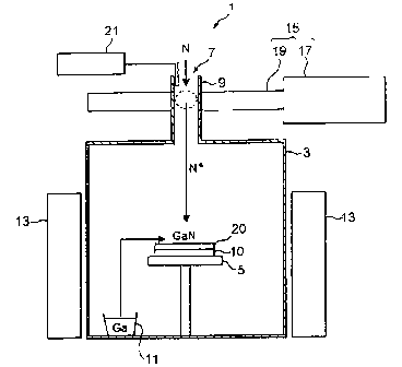
Fig. 1 is a view showing a vapor phase growth apparatus
1 for growing a group III-v nitride semiconductor in
accordance with this embodiment. The vapor phase growth
apparatus 1 of this embodiment is used for growing gallium
nitride (GaN) , which is a group III-V nitride semiconductor,
on a seed crystal 10 made of sapphire and supported on a
19
CA 02313155 2000-06-29
FP00-0068-00
seed crystal support table 5 within a reaction tube ( reaction
ampoule) 3 made of Silica. As depicted, the upper face of
the reaction tube 3 is formed with an inlet port 9 hawing
an inlet 7 for introducing nitrogen (NZ ) , Whereas a container
11 for containing gallium (Ga) , which is a group IIT (group
3B) element, is disposed within the reactiontube3. Further,
the reaction tube 3 is surrounded by a heater 13 for heating
Ga within the container 11, the vicinity of the seed crystal
10, and the reaction tube 3.
For enhancing the uniformity in temperature in the radial
direction of the seed crystal 10, the reaction tube 3 is
made as a vertical furnace. Further, the reaction tube 3
is configured such that it can communicate gases to the outside
only through the inlet 7.
Also, the vapor phase growth appazatus 1 is provided
with an excitation unit 15 for exciting nitrogen introduced
into the inlet port 9 so as to make it attain a plasma state.
The excitation unit 15 is constituted by an oscillator 17
for generating a microwave with a freguency of 2.45 GBz,
and a waveguide 19 through which the microwave from the
oscillatoz 17 propagates. For introducing the microwave
into the inlet port 9, the latter penetrates through the
waveguide 19:
Further, the vapor phase growth apparatus 1 is provided
with a pressure gauge 21 for measuring the pressure therein.
Under the control of a control unit which is not depicted,
CA 02313155 2000-06-29
FP00-0068-00
nitrogen at a flow rate corresponding to the pressure within
the reaction tube 3 measured by the pressure gauge zl is
introduced into the reaction tube 3 by way of the inlet port
9.
With reference to Fig. 1, a method of growing GaN by
use of the vapor phase growth apparatus 1 will now be explained .
Before introducing nitrogen from the inlet port 9, the
heater 13 is initially actuated, such that the temperature
in the vicinity of the seed crystal 10 becomes about 1000°C,
and the temperature of the container 11 fvr Ga becomes about
1100°C. As a consequence, Ga within the container 11 is
evaporated. Also, while the oscillator 17 is actuated so
as to generate a microwave at 2 . 45 GHz, this microwave becomes
a standing wave within the waveguide 19.
Subsequently, nitrogen At a flow rate of about 1 X
10-3 1/min on the basis of its normal gas state with a total
pressure of about 10 Pa to about 4000 Pa is started to be
introduced into the reaction tube 3 from the inlet 7.
Nitrogen would be continuously supplied into the reaction
tube 3 until GaN is completely grown. Also, nitrogen passing
through the inlet port 9 is excited by the microwave advancing
through the waveguide 19, so as to attain a plasma state.
Nitrogen in the plasma state can take various forms such
as atom and molecule form , which will hereinafter be
collectively referred to as nitrogen plasma for convenience .
Also, in the nitrogen plasma, only N~ (nitrogen radical)
21
CA 02313155 2000-06-29
FP00-0068--00
is depicted, without showing ion-like plasmas such as Nz+
and Nz-.
Evaporated Ga and the nitrogen plasma each diffuse so
as to reach the vicinity of the seed Crystal 10. As they
react with each other, a GaN layer 20 can be grown on the
seed crystal 10. Though the partial pressure of nitrogen
within the reaction tube 3 is about to decrease as the GaN
layer 20 grows, the unshown control unit determines the flow
rate of nitrogen introduced into the inlet port 9 according
to the pressure data from the pressure gauge 21 so as to
compensate for the decrease, whezeby the total pressure
within the reaction tube 3 can be kept substantially constant .
Therefore, theGaN layer 20 can be grown stably. Furthermore,
because the reaction tube 3 is heated by the heater 13 , the
GaN is not grown on the inner wall of the reaction tube 3
but on the seed crystal 10.
In this embodiment, since nitrogen within the reaction
tube 3 is excited so as to attain a plasma state which is
highly reactive, it is more likely to react with Ga as compared
with a nitrogen molecule (Nz) state.in Which the bonding
strength between atoms is higher, and it can successively
be introduced into the reaction tube 3 unlike the case
employing the closed ampoule method, whereby the growth rate
of the GaN layer 20 can be enhanced. Experiments carried
out by the inventors have revealed that, while the growth
rate of GaN layer was 1 ~m/hr or less when nitrogen was not
22
CA 02313155 2000-06-29
FP00-0068-00
excited so as to attain the plasma state, it was about 100
,c~m/hr in accordance with the method of this embodiment . Also,
since only Ga and nitrogen, which are components of the GaN
layer 20, are used as the raw materials for GaN in this
embodiment, it is not necessary to let out gases from~within
the reaction tube 3 as in the open ampoule method employed
in the hydride vapor epitaxy growth method and organic metal
vapor epitaxy growth method, whereby the material ef f iciency
can be improved. Here, according to experiments carried out
by the inventors, substantially all of nitrogen introduced
into the reaction tube 3 contributed to crystal growth,
whereby the material efficiency was 80% or higher.
If an AlGaN layer, an InGaN layer, and the like are
laminated on a substrate made of thus grown GaN, then a blue
LED and the like can be manufactured. If the chip surface
of such a blue LED is coated with a YAG type phosphor, then
a white LED can be realized.
Second Embod nt
With reference to Fig. 2, a second embodiment of the
group III--V nitride semiconductor groGrthmethod in accordance
with the present invention will now be explained. In this
embodiment, a vapor phase growth apparatus 1 similar to that
of the first embodiment is used.
For growing a GaN layer 20 by the growth method of this
embodiment, nitrogen (Nz) is initially started to be
introduced into the reaction tube 3 by way of the inlet port
23
CA 02313155 2000-06-29
FP00-0068-00
9, and then hydrogen (Hz) is introduced therein by a
predetermined amount. Nitrogen is cpntinuously supplied
into the reaction tube 3 until GaN is completely grown.
Subsequently, as in the first embodiment, Ga within the
container 11 is evaporated, and also nitrogen introduced
from the inlet 7 is excited so as to become a nitrogen plasma.
Then, as shown in Fig. 2, the nitrogen plasma and hydrogen
react with each other, whereby NHx ( x = 1, 2 , 3 ) , ions thereof ,
their plasma-state products, and the like are generated.
These will hereinafter be referred to as NHX. While there
are cases where hydrogen within the reaction tube 3 flows
into the inlet port and thezeby attains a plasma state,
"reaction between the nitrogen plasma and hydrogen" in this
embodiment encompasses the case where thusgenerated hydrogen
plasma and the nitrogen plasma react with each other.
Then, NHx having reached near the seed crystal 10 and
evaporated Ga react with each other, whereby the GaN layer
grows on the seed crystal 10. Here, since nitrogen flows
so as to diffuse into the vicinity of the seed crystal 10
20 and reacts with Ga, it is more likely to react with Ga as
compared with a nitrogen molecule (Nz) state in which the
bonding strength between atoms is higher, and it can
successively be introduced into the reaction tube 3 unlike
the case employing the closed ampoule method, whereby the
growth rate of the GaN layer 20 can be enhanced. In practice,
when an experiment was carried out with the amount of
24
CA 02313155 2000-06-29
FP00-0068-00
introduction of hydrogen being set to 30~ with respect to
the total gas content within the reaction tube 3, the growth
rate of GaN layer 20 was about 150 ~Gem/hr.
When the GaN layer 20 is grown by the reaction between
NHx and Ga, hydrogen (HZ), which is no component of GaN, is
generated. Since the vapor phase growth apparatus 1 of this
embodiment is provided with no outlet, thus generated
hydrogen is not let out . Then, thus generated hydrogen ( Hj j
and the nitrogen plasma newly supplied into the reaction
tube 3 by way of the inlet port 9 are caused to react with
each other, so as to generate again the hydride of nitrogen
and its ions . Thereafter, thus generated NHx and evaporated
Ga react with each other, Whereby the GaN layer 20 on the
seed crystal 10 can further be made thicker. Namely, since
hydrogen ( Hi j . which is no component of GaN, can be repeatedly
utilized as being circulated within the reaction tube 3,
it is unnecessary to let out the gases fromwithin the reaction
tube 3, whereby the material efficiency can be improved.
In practice, when the GaN layer was grown by the method of
2o this embodiment, the material efficiency was about 80%.
Though the partial pressure of nitrogen within the
reaction tube 3 is about to decrease as the GaN layer 20
grows, the unshown control unit determines the flow rate
of nitrogen introduced into the in7.et part 9 according to
the pressure data fromthe pressure gauge 21 so as to compensate
for the decrease, as in the first embodiment, whereby the
CA 02313155 2000-06-29
FP00-0068-00
total pressure within the reaction tube 3 can be kept
substantially constant. Therefore, the GaN layer 20 can be
grown stably.
T~ ird Embodiment
With reference to Fig. 3, a third embodiment of the
group III-V nitride semiconductor growthmethod in accordance
with the present invention will now be explained. In this
embodiment, a vapor phase growth apparatus 1 similar to that
of each of the above-mentioned embodiments is used.
First, nitrogen introduced from the inlet 7 is excited
so as to become a nitrogen plasma, and the heater 13 is actuated
so as to evaporate Ga. Nitrogen is continuously introduced
into the reaction tube 3 until GaN is completely grown.
Subsequently, hydrogen chloride (HC1), which is a halide,
,15 is introduced into the reaction tube 3 from the inlet 7 by
a predetermined amount at a partial pressure of 10 Pa to
500 Pa. Then, HCl having flowed to the bottom part of the
reaction tube 3 under the influence of partial pressure reacts
with Ga within the container 11, whereby gallium chloride
( GaCl ) , which is a halide of the group III element, and hydrogen
(a=) are generated. Further, due to the difference in vapor
pressure between the vicinity of the container li and the
vicinity of the seed crystal 10, GaCl and H~ reach the seed
crystal 10. Then, as the above-mentioned nitrogen plasma
and GaCl react with each other, a GaN layer 20, which is
a group III-V nitride semiconductor, is grown on the seed
26
CA 02313155 2000-06-29
FP00-0068-00
crystal 10.
Here, since nitrogen is excited so as to become a
nitrogen plasma, it is more likely to react with Ga as compared
with a nitrogen molecule (NZ) state in which the bonding
strength betureen atoms is higher, and it can successively
be introduced into the reaction tube 3 unlike the case
employing the closed ampoule method, whereby the growth rate
of GaN layer 20 can be enhanced. Further, since Ga is
transported to the vicinity of the seed crystal 10 as GaCl,
which is a halide having a high equilibrium vapor pressure,
its transportation speed becomes faster than that in the
case where Ga is evaporated so as to reach the vicinity of
the seed crystal 10 as in the first and second embodiments,
whereby the growth rate of GaN layer 20 can be enhanced.
In practice, when an experiment was carried out with the
amount of introduction of HC1 being set to 10~ with respect
to the total gas content within the reaction tube 3, the
growth rate of GaN layer 20 was about 160 ,um/hr.
On the other hand, the halogen (C1), which is no
component of GaN, generated when the GaN layer 20 is grown
by the reaction between the nitrogen plasma and GaCl, and
hydrogen (H2) introduced from the inlet 7 or hydrogen (Hz)
generated at the same time when GaCl is generated react with
each other, whereby hydrogen chloride (HCl) is generated.
Here, there are cases where chlorine does not react with
hydrogen and is generated as a halogen molecule ( Clz ) . Since
27
CA 02313155 2000-06-29
FP00-0068-00
the vapor phase growth apparatus 1 of this embodiment is
provided with no outlet, thus generated HC1 and C12 would
not be let out . Then, thus generated HC1 or Clz reacts faith
Ga disposed within the reaction tube 3, whereby GaCI is
generated again. Thereafter, thus generated GaCl and the
nitrogen plasma can be caused to react with each other, so
as to further thicken the GaN layer. 20 on the seed crystal
. Namely, since the halogen ( Cl ) , which is no component
of GaN, can be repeatedly utilized as being circulated within
10 the reaction tube 3 in this embodiment, it is unnecessary
to let out the gases from within the reaction tube 3, whereby
the material efficiency can be improved.
Not only C1 but also Hr, z, or the like may be used
as the halogen circulated within the reaction tube 3 in this
embodiment . Also, chlorine ( ClZ ) , bromine ( Hr2 ) , iodine ( I2 ) ,
or the like may be introduced into the reaction tube 3 as
a halogen molecule instead of hydrogen chloride (HCl).
Though the partial pressure of nitrogen within the
reaction tube 3 is about to decrease as the GaN layer 20
grows, the unshown control unit determines the flow rate
of nitrogen introduced into the inlet port 9 according to
the pressure data fromthe pressure gauge 21 so as to compensate
for the decrease, as in each of the above-mentioned
embodiments, whereby the total pressure within the reaction
tube 3 can be kept substantially constant, Therefore, the
GaN layer 20 can be grown stably.
28
CA 02313155 2000-06-29
FP00-0068-00
Fourth Embod~.ment
With reference to Fig. 4, a fourth embodiment of the
groupIII-v nitride semiconductor growth method in accordance
with the present invention will now be explained. In this
embodiment, a vapor phase growth apparatus 1 similar to that
of each of the above-mentioned embodiments is used.
For growing a GaN layer 20 by the groGrth method of this
embodiment, nitrogen (Nz) is initially started to be
introduced into the reaction tube 3 by way of the inlet port
9, and then hydrogen chloride (HC1) and hydrogen (Hz) are
introduced therein by a predetermined amount as in the third
embodiment. Nitrogen would be continuously supplied into
the reaction tube 3 until GaN is completely grown.
Subsequently, Ga within the container 11 is evaporated, and
nitrogen introduced from the inlet 7 is excited so as to
become a nitrogen plasma. Then, as shown in Fig. 4, the
nitrogen plasma and hydrogen (Hz) react with each other,
whereby NHx is generated. Also, HCl having flowed to the
bottom part of the reaction tube 3 under the influence of
partial pressure reacts with Ga within the container 11,
whereby gallium chloride (GaCl) , which is a halide of a group
III element, and hydrogen ( HZ ) are generated ( though the f low
of hydrogen at this time is not depicted).
Due to the difference in vapor pressure between the
vicinity of the container 11 and the vicinity of the seed
crystal 10, thus generated GaCl and NHx reach the seed crystal
29
CA 02313155 2000-06-29
FP00-0068-00
10. Then, as GaCl and NHX react with each other, the GaN
layer 20, which is a group III-V nitride semiconductor, is
grown on the seed crystal 10.
Here, since nitrogen flows to the vicinity of the seed
S crystal 10 as NHX, which is a hydride, and reacts with Ga,
it is more likely to zeact with Ga as compared with a nitrogen
molecule (N2) state in which the bonding strength between
atoms is higher, and it can successively be introduced into
the reaction tube 3 unlike the case employing the closed
ampoule method, whereby the growth rate of GaN layer 20 can
be enhanced . Further, since Ga is transported to the vicinity
of the seed crystal 10 as GaCl, which is a halide having
a high equilibrium vapor pressure, its transportation speed
becomes faster than that in the case where Ga is evaporated
so as to reach the vicinity of the seed crystal 10 as in
the first and second embodiments, whereby the growth rate
of GaN layer 20 can be enhanced. In practice, when an
experiment was carried out with the amounts of introduction
of hydrogen and HCl being set to 50~ and lOg with respect
to the total gas content within the reaction tube 3,
respectively, the growth rate of GaN layer 20 was about 200
,t~m/hr .
When the GaN layez 20 is grown by the reaction between
GaCl and NHX, hydrogen (HZ), which is no component of GaN,
and hydrogen Chloride ( HC1 ) , Which is a halide, are geriexated.
Here, there are cases where chlorine does not react with
CA 02313155 2000-06-29
FP00-0068-00
hydrogen and is generated as a halogen molecule ( Cli ) . Since
the vapor phase growth apparatus 1 of this embodiment is
provided with no outlet, thus generated HZ, HC1, and the like
would not be let out. Then, thus generated hydrogen (H2)
and the nitrogen plasma newly supplied into the reaction
tube 3 by way of the inlet port 9 react with each other,
whereby NHx is generated again. On the other hand, hydrogen
chloride (HC1) or chlorine (C1~) and Ga contained in the
container 11 react with each other, whereby GaCl is generated
again.
Thereafter, thus regenerated GaCl and NHx can be caused
to react with each other, so as to further thicken the GaN
layer 20 on the seed crystal 10. Namely, since hydrogen ( HZ )
and the halogen (Clj, which are no components of GaN, can
be repeatedly utilized as being circulated within the
reaction tube 3 in this embodiment, it is unnecessary to
let, out the gases from within the reaction tube 3, whereby
the material efficiency can be improved. In practice, when
the GaN layer was grown by the method of this embodiment,
the material efficiency was 80~ or higher.
Aa in the third embodiment, not only C1 but also Br,
I, or the like may be used as the halogen circulated within
the reaction tube 3 in this embodiment. Also, chlorine (C12 ) ,
bromine (Bri), iodine (IZ), or the like may be introduced
into the reaction tube 3 as a halogen molecule instead of
hydrogen chloride (HC1).
31
CA 02313155 2000-06-29
FP00-0068-00
Though the partial pxessure of nitrogen within the
reaction tube 3 is about to decrease as the GaN layer 20
grows, the unshown control unit determines the flow rate
of nitrogen introduced into the inlet port 9 according to
the pressure data from the pressure gauge 21 so as to compensate
for the decrease, as in each of the above-mentioned
embodiments, whereby the total pressure within the reaction
tube 3 can be kept substantially constant. As a consequence,
the GaN layer 20 improves its yield of single crystallization
and can be grown stably.
Fifth Emb ' xn n
With reference to Fig. 5, a fifth embodiment of the
group III-V nitride semiconductor growth method in accordance
with the present invention will now be explained. This
embodiment differs from the fzrst embodiment in the
configuration of the excitation unit for exciting nitrogen
so as to. make it attain a plasma state . The excitation unit
35 of the vapor phase growth apparatus 1 of this embodiment
comprises two electrodes 30, 30, each shaped like a flexed
plate, opposing each other so as to surround a reaction tube
23; and a high-frequency power source 40 for applying
high-frequency, high voltages between these electrodes 30,
30.
The reaction tube 23 used in this embodiment has
substantially a circular columnar form, whereas an inlet
tube 25 for introducing nitrogen therein is inserted into
32
CA 02313155 2000-06-29
FP00-0068-00
its upper face at the center thereof . The lower part of the
reaction tube 23 is surrounded by a heater 13 similar to
that of the first embodiment. Though not depicted, a seed
crystal 10 and a container 11 for containing Ga are disposed
within the reaction tube 23 as in the first embodiment ( see
Fig. 1).
Fig. 6 is a graph showing voltages applied between the
electrodes 30, 30 by the high-frequency power source 40.
As shown in this graph, the high-frequency power source 40
alternately applies positive and negative pulsed voltages
between the electrodes 30, 30. Also, a break is formed
between individual pulses, whereby aso-called intermittent
signal is generated. Further, each of rise time ti and fall
time t2 is relatively short, i.e., 1.25 ~.tsec, while the
frequency is variable Within the range of 1 kHz to 100 kHz.
Also, the positive and negative pulsed voltages are +8 kv
and -12 kv, thus forming asymmetrical waveforms.
For growing a GaN layer pn the seed crystal 10 in such
a configuration, temperature is initially set in the heater
13 under a condition similar to that in the first embodiment,
so as to evaporate Ga, and then nitrogen is introduced into
the xeaction tube 23 from the inlet tube 25. Nitrogen is
continuously supplied into the reaction tube 23 until GaN
is completely grown. Also, nitrogen having reached between
the electrodes 30, 30 after being introduced into the reaction
tube 23 from the inlet tube 25 is excited by the high-frequency,
33
CA 02313155 2000-06-29
FP00-0068-00
high voltages applied by the high-frequency power source
40, so as to become a nitrogen plasma.
Unlike conventional techniques in which a continuous
sine wave of high-frequency voltage is applied between
electrodes, this embodiment uses a power source applying
positive and negative pulsed voltages with a break between
individual pulses, whereby the discharging phenomenon does
not yield corona discharge, so that nitrogen is likely to
become a nitrogen plasma. Also, since pulse signals have
a high rising speed, the electric field strength per unit
area is high, whereby nitrogen is likely to be excited so
as to become a nitrogen plasma.
Further, since the reaction tube 23 positioned between
the electrodes 30, 30 is formed from silica, which is a
dielectric, an electric field can uniformly be generated
between the electrodes 30, 30. As a consequence, abnormal
discharge can be prevented from occurring, so that plasmas
can be generated more stably and effectively.
While a process using an inactive gas under a low
pressure has conventionally been known as a technique for
plasma discharge, plasmas can be generated even at normal
pressure if the high-frequency power source 40 of this
embodiment is used.
Further, when a microwave is used as in the first
embodiment, it is necessary that the size of the inlet port
9 be made smaller so that the microwave does not leak out
34
CA 02313155 2000-06-29
FP00-0068-00
from the inlet port 9, whereby it requires labor to design
and make the reaction tube 23. In the fifth embodiment, by
contrast, the inlet tube 25 can be foamed with a desirable
size, whereby it becomes easier to design and make the reaction
tube 23.
Though plasmas mainly occur between the electrodes 30,
30, the excitation unit 35 of this embodiment can change
the electrode forms more freely, as shown in Fig. 5 and Figs .
7 to 9 which will be explained in the following, as compared
With other plasma generating means, whose forms are harder
to change, such as those of RF, ECR, and microwaves . Thus,
this embodiment is advantageous in that, while the seed
crystal is disposed at a desirable place, plasmas can be
generated nearby.
Thus excited nitrogen plasma and evaporated Ga each
diffuse so as to reach the vicinity of the seed crystal 10.
As they react with each ether, the GaN layer 20 can be grown
on the seed crystal 10.
With reference to Figs . 7 to 9, modified examples of
this embodiment twill now be explained. In the first modified
example shown in Fig. 7 , one rod-like electrode 30a is inserted
through the upper face of the reaction tube 23, an annular
electrode 30b is disposed around the upper part of the reaction
tube 23, and the high-frequency power souxce 40 is connected
to the rod-like electrode 30a and the annular electrode 30b.
The rod-like electrode 30a is Covered with n dielectric member
CA 02313155 2000-06-29
FP00-0068-00
50a. As with the fifth embodiment, such a configuration can
easily make a plasma out of nitrogen having reached between
the rod-like electrode 30a and annulaz electrode 30b after
being introduced from the inlet tube 25. Also, since the
S dielectric member 50a is disposed between the rod-like
electrode 30a and the annular electrode 30b, an electric
field can uniformly be generated between the rod-like
electrode 30a and the annular electrode 30b. As a consequence,
abnormal discharge can be prevented from occurring, so that
plasmas can be generated more stably and effectively.
In the second modified example shoran in Fig. 8, two
planar electrodes 30c, 30c in parallel are inserted into
the reaction tube 23 from the upper face thereof, whereas
the high-frequency power source 40 is Connected to the planar
electrodes 30c, 30c. Also, a planar dielectric member 50b
is attached to each of the planar electrodes 30c, 30c on
the opposing surface side thereof. As with the fifth
embodiment, such a configuration can easily make a plasma
out of nitrogen having reached between the planar electrodes
30c, 30c after being introduced from the inlet tube 25. Also,
since the planar dielectric member 50b is disposed between
the planar electrodes 30c, 30c, an electric field can
uniformly be generated between the planar electrodes 30c,
30c. As a consequence, abnormal discharge can be prevented
from occurring, so that plasmas can be generated more stably
and effectively.
36
CA 02313155 2000-06-29
FP00-0068-00
In the third modified example shown in Fig. 9, a
cylindrical support rod Z7 is inserted into the reaction
tube 23 from the upper face thereof, whereas a disk electrode
30d is attached to the lower end of the support rod 27. The
seed crystal 10 is attached to the lower face of the disk
electrode 30d. Further, in this modified example, the
container 11 is disposed so as to oppose the disk electrode
30d, whereas the disk electrode 30d and~Ga within the container
11 are electrically connected to the high-frequency power
source 40. Namely, Ga within the container 11 is used as
an electrode. As with the fifth embodiment, such a
configuration can easily make a plasma out of nitrogen having
reached between the disk electrode 30d and container 11 after
being introduced from the inlet tube 25. In this modified
example, the GaN layer 20 would be grown under the seed crystal
10.
Though the fifth embodiment is configured such that
high-frequency, high voltages are applied between two
electrodes in the first embodiment so as~to generate plasmas,
it is also applicable to the second to fourth embodiments.
If the technique of the fifth embodiment is applied to the
third embodiment, then nitrogen can easily be turned into
a plasma. If this technique is applied to the second and
fourth embodiments, then nitrogen and hydrogen ran easily
be caused to react with each other upon plasma excitation.
Though the invention achieved by the inventors is
37
CA 02313155 2000-06-29
FP00-006$-00
specifically explained with reference to the embodiments
in the foregoing, the present invention should not be
restricted to the above-mentioned embodiments. For example,
using aluminum (Al ) , indium ( In ) , and the like as group III
elements, the group III-V nitride semiconductor growth
apparatus of the present invention can grow group III-V
nitride semiconductors such as A1N, InN, and the like in
addition to GaN.
As explained in the foregoing, the group III-V nitride
semiconductor growth method and vapor phase growth apparatus
in accordance with the present invention can yield a higher
material efficiency and a higher growth rate.
38