Note: Descriptions are shown in the official language in which they were submitted.
CA 02313442 2000-07-06
Optoelectronic component group
Technical field
The invention relates to an optoelectronic component
group in accordance with the preamble of Claim 1. This
concerns, in particular, LED arrays which are arranged
in a planar manner, for example surface lighting
luminaires.
Prior art
WO 99/07023 has already disclosed an optoelectronic
component group in which a chip support has external
connecting parts for the purpose of heat dissipation.
However, this arrangement is very complicated and
expensive and takes up a lot of space.
EP-A 99 100 352.6 has disclosed a surface lighting
luminaire with a common support on which a plurality of
LEDs form a planar array. In EP-A 900 971, the support
used is a glass plate on which conductor tracks are
also fitted.
Summary of the invention
The object of the present invention is to provide an
optoelectronic component group in accordance with the
preamble of Claim 1 which realizes good heat
dissipation in a simple, cost-saving and space-saving
manner.
This object is achieved by means of the characterizing
features of Claim 1. Particularly advantageous
refinements can be found in the dependent claims.
' CA 02313442 2000-07-06
- 2 -
Since LEDs heat up, care must be taken to ensure that
the thermal load is kept as small as possible. This
problem arises particularly when a plurality of LEDs
are combined to form a section, as in the case of a
lamp for example, or an array, as in the case of a
surface lighting luminaire for example. To date, care
has always had to be taken to ensure that the packing
density of the LEDs is not chosen to be too close. The
minimum distance that has been customary heretofore is
8 to 10 mm (in other words about 1 LED/cm2), in order
to keep the extent of mutual heating as small as
possible. This is because excessively great heating,
beyond the junction temperature of the LED chip, leads
to shortening of the service life through to
destruction. The previous relatively large minimum
distance guarantees that each LED only has to cope with
its inherent heat. In order nevertheless to produce a
homogeneously illuminated surface, reflectors have been
used heretofore. In addition, a diffusing screen is
applied as a covering. These parts necessitate
additional costs.
According to the invention, a material which has a good
heat dissipation (better than the conventional printed
circuit board material such as FR 1 to 4 or CEM 1) is
now used as the support for the component group
containing LEDs. In particular, a ceramic substrate of
the kind already known per se in the semiconductor
industry (based on aluminium oxide or else A1N), non-
conducting cermet or composite material is suitable for
this purpose. This includes both a material mixed from
two components (for example epoxy resin with inorganic
filling material), and a material with a layer
structure (for example ceramic as upper layer
(aluminium oxide) and metal (aluminium) as lower
layer) .
This means that it is. riow possible to dispense partly
or even entirely with reflectors, depending on the
CA 02313442 2000-07-06
- 3 -
desired degree of homogeneity. With a relatively large
distance (3 to 5 mm) between the LEDs, it is
advantageous also to continue to use a diffusing screen
as a covering. A covering is in any case advisable or,
under certain circumstances, even dictated by
regulation, depending on the application. However, the
diffusing screen is no longer absolutely necessary,
since the distance between the LEDs can, owing to the
good heat dissipation, be chosen to be very small, in
particular below 2 mm, down to values of about 1 mm.
Overall, according to the invention, the heat
dissipation is essentially effected by way of the
support material. The packing density of the LEDs can
thereby be increased. Instead of 1 LED/cm2, packing
densities of typically up to 4 LED/cm2 or higher are
now possible.
In detail, the present invention relates to an
optoelectronic component group which is mounted on a
support and which comprises at least two adjacent LEDs
at a prescribed distance (a), and also associated
connecting lines, where the support is composed of a
material having a thermal conductivity of better than
1 W/Kxm, in particular of at least 1.5 W/Kxm.
Preferably, the support is composed of a material which
can be populated by means of SMD technology. In
particular, the support is composed of a material which
is selected from the group consisting of ceramic, non-
conducting cermet, plastic and/or composite material,
where further, in particular electronic component parts
may be integrated on the support.
Given a suitable choice of the material, at least one
further component can be fixed on the support. This
component may be an electronic circuit, in particular
an integrated circuit or complete drive circuit, or one
to a plurality of LEDs. A component group of this type
CA 02313442 2000-07-06
- 4 -
may, in particular, be a component part of a surface
lighting luminaire or lamp.
The LEDs on the support are usually arranged regularly.
By way of example, they form a section or an array,
with a prescribed distance (a and b) in the rows and
columns, respectively. The row and column distances
may, in particular, be identical.
The essential consequence of the suitable choice of the
support material is the considerably reduced distance
between two adjacent LEDs. It is at most 5 mm,
preferably less than 2 mm.
For special applications, the support may be mounted on
a further heat-dissipating material, in particular a
separate thermal plate or body part of a vehicle.
In a particularly preferred embodiment, the structural
height of the group is less than 10 mm, which is of
considerable importance principally for surface
lighting luminaires.
A further embodiment is an optoelectronic component
group which is mounted on a support and which comprises
at least two adjacent LEDs, which are spaced apart from
one another, and also associated connecting lines. The
support is composed of a material which dissipates heat
well enough to realize a distance between adjacent LEDs
of at most 5 mm, preferably less than 2 mm, without
limiting the specified forward current of the LEDs (for
example 70 mA in the case of TOPLED) and without
further aids such as, for example, cooling fins.
In a particularly preferred embodiment, the support
material is mounted on other heat dissipators (for
example a separate thermal plate), with the result that
the heat dissipation is additionally improved. This
applies, in particular, when the component group is
CA 02313442 2000-07-06
used as a rear luminaire for vehicles, in which case
sheet-metal body parts can perform the function of the
additional heat dissipator.
By virtue of this mounting possibility, the LEDs can
now be loaded up to the uppermost limit that is
physically possible, the junction temperature. On the
other hand, the luminance can also be increased because
the forward current IF of the LED can be increased.
A crucial advantage of the present invention is that,
on the readily thermally conductive support, in
particular a ceramic support, further structural parts
or components can also additionally be constructed and,
in particular, can even be integrated with the LEDs, in
particular electronic circuits. By way of example,
ceramic material is highly suitable as a basis for the
integration of integrated circuits. Such circuits are
required in any case for many applications; by way of
example, protective circuits, monitoring functions and
interfaces to bus systems are involved.
Extremely high compaction is possible as a consequence.
This makes it possible for example to reduce the wiring
harness in a car to one data line and one supply line.
In this case, the drive circuit is concomitantly
applied to the (ceramic) support.
Figures
The invention will be explained in more detail below
using a number of exemplary embodiments. In the
figures:
Figure 1 shows a surface lighting luminaire with LEDs;
Figure 2 shows a further exemplary embodiment of a
surface lighting luminaire in which a circuit
is integrated.
CA 02313442 2000-07-06
- 6
Description of the drawings
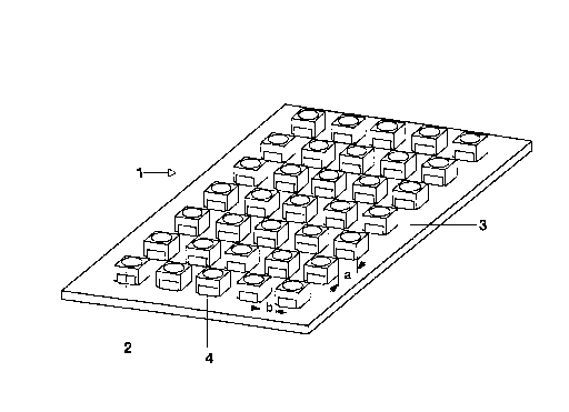
Figure 1 shows a component group 1 comprising a
rectangular array of white LEDs 2 which enable a
surface to be illuminated homogeneously. The associated
connecting lines (4) are illustrated in a greatly
simplified manner. The~LEDs used are forward-radiating
LEDs (for example SMT TOPLED from Siemens). The common
support 3 is composed for example of a ceramic
material, such as aluminium oxide, or of a composite
material such as HITT Plate from DENKA Chemicals. The
latter material is composed of a lower layer of
aluminium, a thermally conductive upper dielectric
layer made of epoxy resin (typical printed circuit
board material) with inorganic filling constituents and
also possibly locally of a thin covering layer made of
copper. The table below shows a comparison of the
thermal conductivity of various substances (at 20°C).
Material CEM 1 A1z03 HITT Plate Quartz Aluminium
(DN 9103)and K-1 glass and
and AlN and Copper
FR 2 HITT Plate
(DN 8033) TH-1
Type Printed Ceramic Composite Glass Metal
circuit material
board
Thermal 0.26 ca. 30 1.8 0.1 220
conduc- and and and and
tivity 0.24 ca. 170 3.5 384
(in W/Kxm)
Table 1
All electrically insulating substances having a
correspondingly high thermal conductivity of at least
1 W/Kxm, preferably 1.5 W/Kxm, in particular at least
3 W/Kxm (ceramic or epoxy resin with inorganic filling
material, in particular with the smallest possible
porosity in each case) are suitable, but electrically
CA 02313442 2000-07-06
conductive substances such as metals are not suitable,
since short circuits would otherwise occur. In the case
of composite materials, it is important that at least
the surface facing the LEDs is electrically insulating
(apart, possibly, from a local conductive covering
layer).
The LEDs 2 are soldered onto the support, which has a
rectangular basic form, using SMD technology.
Additional components such as reflectors are not
required because the distance between the LEDs is only
1.5 mm on each side of the rectangular housing.
Figure 2 shows a further surface lighting luminaire 5,
in which, in addition to an array of LEDs 6, an
integrated circuit 7 is also applied on the ceramic
board forming the support 8. In order to ensure
homogeneous emission in this case, the covering 9 is
embodied as a diffusing screen. This luminaire has a
base area of about 4x3 cm2.
Owing to the narrow distance a (row distance) and b
(column distance) between the LEDs, the structural
height of the housing of the luminaire can be
drastically reduced, to be precise by about 30 to 50g,
compared with conventional technology. This is because
there is approximately a linear relationship between
the lateral distance and the structural height.
Approximately a structural height of 15 mm has to be
observed given a lateral distance of 10 mm, while the
structural height can be reduced to approximately 7 mm
given a distance of a = 5 mm and b = 4 mm.