Note: Descriptions are shown in the official language in which they were submitted.
CA 02313611 2000-07-05
SEMICONDUCTOR DEVICE
BACKGROUND OF THE INVENTION
The present invention relates to a semiconductor
device including a plurality of semiconductor chips
mounted on a substrate, and particularly to a
semiconductor device suitable for realizing the reduction
in size and weight of electronic equipment and the
improvement of performances of the electronic equipment.
Recently, to reduce sizes of semiconductor chips
and increase the level of integration of the
semiconductor chips, a technology of mixedly mounting a
logic circuit, an analog circuit, and memories such as a
DRAM and a flash memory on the same silicon substrate has
been proposed and partially put into practical use.
The technology of mixedly mounting semiconductor
chips on the same silicon substrate, however, has various
technical problems caused by evolution of a process of
fabricating each of the semiconductor chips.
For example, a thermal process necessary for
forming a DRAM capacitor causes a problem in impairing an
ultra-shallow junction profile essential for realizing a
finer structure of a transistor in a logic chip, and also
causes a problem in allowing boron in a gate electrode of
1
CA 02313611 2000-07-05
a P-channel transistor to pass through a gate insulating
film, to make a channel profile of the P-channel
transistor different from a design profile, thereby
degrading the current characteristics of the transistor.
An analog circuit, which interfaces with external
chips such as a driver, an amplifier and sensor, requires
a higher withstand voltage and a higher input range than
those of an advanced CMOS, and accordingly, the analog
circuit is hard to be made finer in its geometrical
structure. For a semiconductor chip in which the above
analog circuit is integrated with a logic LSI required to
be made very finer in its geometrical structure, most of
the semiconductor chip is occupied by the analog circuit
hard to be reduced in its area, to reduce an economical
merit obtained by mixed mounting of the analog circuit
and the logic circuit.
In addition to the above technology of mixedly
mounting semiconductor chips on the same silicon
substrate, a technology of mixedly mounting semiconductor
chips on a package level has been also positively
promoted.
A so-called chip-on-chip structure including
semiconductor.chips simply stacked to each other is
advantageous in shortening lengths of interconnections;
2
CA 02313611 2000-07-05
however, it is disadvantageous in sacrificing
reinforcement of power source lines and ground lines in
the chips. In an ultra-high speed CPU or DSP, an
excessive current flowing in a chip reduces an effective
inner voltage due to resistances of a power supply line
and a ground line, to thereby reduce the operational
speed.
Even for a low power chip desired to realize
operation at a significantly low supply voltage, the
performance thereof may be significantly degraded by a
slight reduction in potential due to resistances of
interconnections. In particular, a chip desired to be
operated at a voltage being as significantly low as 1 V
or less, for example, a chip having a structure using an
SOI (Si on insulator) substrate requires a very stable
power supply line and a very stable ground line.
Against such a background, power supply lines and
ground lines of chips have been conventionally formed
from multi-level interconnections, and in recent years, a
technology of forming bonding pads corresponding to a
plurality of power supply lines and ground lines in chips
and connecting them to interconnections formed in a
substrate, thereby further stabilizing the power supply
lines and ground lines of the chips has been put in
3
CA 02313611 2000-07-05
practical use.
SUMMARY OF THE INVENTION
An object of the present invention is to provide a
semiconductor device capable of mixedly mounting a logic
chip, an analog chip, a memory chip, etc. by stacking
them to each other while stabilizing power supply lines
and ground lines of the chips.
To achieve the above object, according to the
present invention, there is provided a semiconductor
device including: an intermediate substrate having a
conductive portion and also having, on its one surface,
an external connection terminal conducted to the
conductive portion; and semiconductor chips each having
connection portions, the semiconductor chips being
mounted on both the surfaces of the intermediate
substrate; wherein at least two of the semiconductor
chips are electrically conducted to each other via the
conductive portion of the intermediate substrate; and at
least one of a power supply line, a ground line, and a
signal line of each of the semiconductor chips is
connected to the conductive portion of the intermediate
substrate via two or more, conducted to each other, of
the connection portions.
4
CA 02313611 2000-07-05
With this configuration, since semiconductor chips
such as a logic chip, an analog chip, a memory chip, etc.
are mounted on both the surfaces of the intermediate
substrate, it is possible to realize the mixed mounting
of the semiconductor chips, and since at least one of the
power supply line, ground line and signal line of each of
the semiconductor chips thus mounted is connected to the
conductive portion of the intermediate substrate via two
or more, conducted to each other, of the connection
portions, it is possible to stabilize the power supply
lines, ground lines and signal lines of the semiconductor
chips.
BRIEF DESCRIPTION OF THE DRAWINGS
Fig. 1 is a side view showing a schematic
configuration of one embodiment of a semiconductor device
of the present invention;
Figs. 2A and 2B are bottom views each showing a
configuration of connection portions of a semiconductor
chip;
Fig. 3A is a bottom view showing connection
portions of a logic chip and a conductive pattern of the
connection portions, and Fig. 3B is a plan view showing
the surface of an intermediate substrate;
CA 02313611 2000-07-05
Fig. 4 is a sectional side view of an essential
portion of the intermediate substrate illustrating an
example of multi-level interconnections of the
intermediate substrate;
Fig. 5 is a sectional side view showing a schematic
configuration of another embodiment of the semiconductor
device of the present invention;
Fig. 6 is a side view showing a schematic
configuration of one variation of the embodiment of the
semiconductor device of the present invention shown in
Fig. 1;
Fig. 7 is a side view showing a schematic
configuration of another variation of the embodiment of
the semiconductor device of the present invention shown
in Fig. 1; and
Fig. 8 is a side view showing a schematic
configuration of a further variation of the embodiment of
the semiconductor device of the present invention shown
in Fig. 1.
DETAILED DESCRIPTION OF THE PREFERRED EMBODIMENTS
Hereinafter, an embodiment of a semiconductor
device of the present invention will be described in
detail with reference to the drawings.
6
CA 02313611 2000-07-05
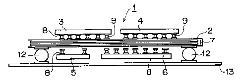
Fig. 1 is a view showing one embodiment of a
semiconductor device of the present invention. In this
figure, reference numeral 1 designates a semiconductor
device. The semiconductor device 1 is a system LSI in
which an analog chip 3 and a DRAM chip 4 are mounted on
one surface of an intermediate substrate 2 as shown in
Fig. 2A, and a high frequency LSI chip 5 and a logic chip
6 having a structure using an SOI substrate are mounted
on the other surface of the intermediate substrate 2 as
shown in Fig. 2B.
These semiconductor chips 3, 4, 5 and 6 may be each
fabricated in accordance with a process optimized for
each device category in consideration of its performance,
cost, and level of integration. To be more specific, the
logic chip 6, which requires high-speed and low power
consumption operation at a low voltage, may be fabricated
on the basis of a scaling law by using an advanced CMOS
logic process allowing high level of integration.
The DRAM chip 4 may be fabricated by using a
general purpose DRAM process capable of realizing a large
capacity at the least cost.
The analog chip 3, which requires a higher
withstand voltage and a higher input range in .
consideration of the interface relationship with
7
CA 02313611 2000-07-05
peripheral chips, may be fabricated by a process which is
required not to involve an advanced processing technology
but to fabricate the chip at a cost lower than that of
the logic chip.
The use of the semiconductor chips 3, 4, 5 and 6
fabricated in accordance with the processes optimized as
described above, allows realization of a system LSI
capable of keeping the performance and cost in balance.
The connection structure of the semiconductor
device 1 will be more fully described below. The
intermediate substrate 2 has a conductive portion
configured as multi-level interconnections 7 made from
copper, and each of the semiconductor chips 3, 4, 5 and 6
has connection portions 8. The semiconductor chips 3, 4,
and 6 are connected to both the surfaces of the
intermediate substrate 2 via the connection portions 8,
and further, the electrical connection between these
chips, that is, the electrical connection between power
supply lines, ground lines and signal lines (not shown)
of the chips are performed by the multi-level
interconnections 7 of the intermediate substrate 2 via
the connection portions 8.
The connection portions 8 of each of the
semiconductor chips 3, 4, 5 and 6 are configured by
8
CA 02313611 2000-07-05
bonding pads which are disposed, on the back surface of
the chip, into an array along the vertical and horizontal
directions as shown in Figs. 2A and 2B. In this
embodiment, these connection portions 8 are connected to
the multi-level interconnections 7 of the intermediate
substrate 2 by means of solder ball bumps 9 as shown in
Fig. 1.
The connection portions 8 of each of the
semiconductor chips 3, 4, 5 and 6 are separated into
groups connected to the power supply line, ground line,
and signal line of the chip, and each group of the
connection portions 8 are conducted to each other in the
chip. In an example of the logic chip 6 shown in Fig. 3A,
a number of the connection portions 8 disposed into an
array are separated into groups connected to the power
supply line, ground line, and signal line. The group of
the connection portions 8 connected to the power supply
line are conducted to each other by means of a conductive
pattern 10 formed in the silicon substrate. The group of
the connection portions 8 connected to the ground line
are conducted to each other by means of a conductive
pattern 11 formed in the silicon substrate. The group of
the connection portions 8 connected to the signal line
(not shown) are conducted to each other by means of a
9
CA 02313611 2000-07-05
conductive pattern (not shown) formed in the silicon
substrate.
The group of the connection portions 8 formed by
the bonding pads, which are conducted to each other by
means of the conductive pattern 10 or 11 as described
above, are generally called "an area pad", which means
that the group of the connection portions 8 form one
areal pad as a whole.
As shown in Fig. 3B, interconnection patterns l0a
and lla conducted to the multi-level interconnections 7
are formed on the surface of the intermediate substrate 2
in such a manner as to be matched to the conductive
patterns 10 and 11 on each of which the group of the
connection portions 8 are disposed, respectively. The
conductive patterns 10 and 11 are conducted to the
corresponding interconnection patterns l0a and lla via
the connection portions 8.
According to this embodiment, since each of the
semiconductor chips 3, 4, 5 and 6 is connected to the
intermediate substrate 2 by means of the connection
portions 8 of the so-called area pad structure, the
contact between the chip and the intermediate substrate 2
is not point-contact but nearly area-contact, to reduce
the connection resistance therebetween, thereby
CA 02313611 2000-07-05
stabilizing the power supply line, ground line, and
signal line of the chip.
In general, the interconnection patterns 10a and
lla of the intermediate substrate 2 and the multi-level
interconnections 7 connected thereto are sufficiently
lower in resistance than the interconnections in each of
the semiconductor chips 3, 4, 5 and 6. Accordingly, since
the interconnections of each of the semiconductor chips 3,
4, 5, and 6 are connected to the multi-level
interconnections 7 via the interconnection patterns 10a
and 11a, a reduction in supply voltage of the chip due to
the interconnection resistance increased by a large
current applied to the interior of the chip can be
significantly improved.
The power supply lines, ground lines, and signal
lines of the semiconductor chips 3, 4, 5, and 6 thus
electrically connected to the intermediate substrate 2
are collected via the multi-level interconnections 7 to a
plurality of external connection terminals 12 provided at
a peripheral portion of one surface of the intermediate
substrate 2. These external connection terminals 12 are
used for mounting the semiconductor device 1 to a printed
wiring board 13 while being connected to wiring portions
(not shown) of the printed wiring board 13. With this
11
CA 02313611 2000-07-05
configuration, the power supply lines, ground lines, and
signal lines of the semiconductor chips 3, 4, 5, and 6
are connected to the wiring portions of the printed
wiring board 13 via the connection portions 8 of the
chips, interconnection patterns l0a and 11a of the
intermediate substrate 2, multi-level interconnections 7,
and the external connection terminals 12, and are
connected to wiring portions of electric equipment on
which the printed wiring board 13 is mounted.
The configuration of the multi-level
interconnections 7 will be described with reference to an
example shown in Fig. 4, in which the DRAM chip 4
configured as a general purpose DRAM bare chip is mounted
on the upper surface of the intermediate substrate 2, and
the logic chip 6 is mounted on the back surface of the
intermediate substrate 2. In this example, since the
connection portions 8 (interface terminals) of the DRAM
chip 4 are partially deviated from the connection
portions 8 of the logic chip 6, the interconnections of
these chips 4 and 6 must be connected to the
interconnections of the intermediate substrate 2 in such
a manner as to correct the above positional deviation
between both the chips 4,and 6.
The multi-level interconnections 7 shown in Fig. 4
12
CA 02313611 2000-07-05
can connect the chips to each other via the
interconnection patterns (not shown) formed on the
surface of the intermediate substrate 2 in such a manner
as to enhance the degree of freedom in connection and
minimize the connection lengths.
Even in this example, the semiconductor chips 4 and
6 are mounted to the intermediate substrate 2 by
connecting solder ball bumps 9 to the connection portions
8 configured as the bonding pads.
According to the semiconductor device 1 having the
above configuration, since the semiconductor chips 3, 4,
5, and 6 are mounted on both the surfaces of the
intermediate substrate 2, it is possible to mixedly mount
different semiconductor chips such as the logic chip 3,
DRAM chip 4, high frequency LSI chip 5, and logic chip 6
and hence to reduce the size of the semiconductor device
1 and increase the level of integration of the
semiconductor device 1.
Since the power supply line, ground line, and
signal line of each of the semiconductor chips 3, 4, 5
and 6 thus mounted are each connected to the multi-level
interconnections 7 of the intermediate substrate 2 via a
group, conducted to each other, of the connection
portions 8, the contact between the chip and the
13
CA 02313611 2000-07-05
intermediate substrate 2 is not point-contact but nearly
area-contact, to reduce the connection resistance
therebetween. This makes it possible to significantly
reduce a potential drop due to the resistances of the
interconnections of the chip, thereby stabilizing the
power supply line, ground line, and signal line of the
chip.
To be more specific, for a conventional
semiconductor chip in which a power supply line or a
ground line made from copper having a thickness of 1.5 gm
and a width of 100 gm is used as an interconnection on
the uppermost layer, the resistance per unit
interconnection length (10 mm) is 1.3 Q, and a potential
drop caused when a current of 500 mA is applied to the
interconnection reaches 0.65 V. Accordingly, it is
difficult to design a low power LSI operable at a voltage
being as small as 1 V.
On the contrary, in the embodiment of the present
invention shown in Fig. 1, the resistance per unit length
(10 mm) of the interconnection on the intermediate
substrate 2 having a thickness of 50 gm and a width of
100 Ilm is 36 mQ, and a potential drop when a current of
500 mA is applied to the interconnection is suppressed at
18 mV.
14
CA 02313611 2000-07-05
The interconnection layers of the semiconductor
chips are connected to the intermediate substrate 2 with
a pitch of 300 k4m, the maximum potential drop is about 28
mV (0.65 V x0.3 mm/10 mm/2 + 18 mV). Accordingly, since
the potential drop is very smaller, it is possible to
design a low power LSI operable at a voltage being as
small as 1 V.
The terminal capacitance upon conventional board
mounting is about 10 pF; however, the interconnection
capacitance between both chips mounted on the
intermediate substrate 2 becomes one-fifth the terminal
capacitance, more concretely, about 2 pF per unit
interconnection distance (10 mm).
The reduction in power has been achieved by mixedly
mounting a DRAM; however, according to the present
invention, it is possible to achieve the reduction in
power comparable to that obtained in the case of mixedly
mounting the DRAM by connecting a specialized logic chip
6 to a specialized DRAM chip 4 with the above low
interconnection capacitance.
Since the power supply line, ground line, and
signal line are each stabilized, a chip having the
structure using an SOI substrate, which is mounted as the
logic chip 6, can be operated at a voltage being very
k 15
CA 02313611 2000-07-05
lower than 1 V. Further, since the capacitance of a BUS
equivalent to mixed mounting of a DRAM chip can be
reduced, there can be obtained a device structure
expected to minimize the power consumption.
While the connection portions 8 of the
semiconductor chips 3, 4, 5 and 6 are connected to the
intermediate substrate 2 by means of the solder ball
bumps 9 in the above embodiment, the present invention is
not limited thereto. For example, the connection portions
8 may be connected to the intermediate substrate 2 by
means of an anisotropic conductive film (ACF) 14 as shown
in Fig. 5. The anisotropic conductive film 14 allows
electric connection between the connection portions 8 and
the intermediate substrate 2 by applying heat and
pressure thereto. The use of the anisotropic conductive
film 14 allows a region in which the connection portions
8, that is, the bonding pads are present to be made
electrically conductive in the vertical direction, and
also allows adjacent two of the connection portions 8 to
be significantly simply separated from each other.
The conductive portion of the intermediate
substrate 2 is not limited to the multi-level
interconnections 7 but may be a single layer
interconnection.
16
CA 02313611 2000-07-05
~
Figs. 6 to 8 show variations of the semiconductor
device shown in Fig. 1. In the variation shown in Fig. 6,
semiconductor chips 3, 4, 5, and 6 are mounted, on the
flip-chip basis, on an intermediate substrate 2 and are
sealed with a resin 15, to form a semiconductor device,
and the semiconductor device is mounted, on the flip-chip
basis, on a printed wiring board 13 positioned outside
the intermediate substrate 2 by means of external
connection terminals 12 provided at a peripheral portion
on one surface of the intermediate substrate 2. With this
structure, since the semiconductor chips 3, 4, 5, and 6
are mounted, on the flip-chip basis, on the intermediate
substrate 2 and the semiconductor device thus obtained is
directly mounted, on the flip-chip basis, on the printed
wiring board 13, it is possible to suppress the overall
height of the semiconductor device, and hence to realize
high density mounting of the semiconductor device.
The variation shown in Fig. 7 is different from
that shown in Fig. 6 in that an additional substrate 16
is provided between the intermediate substrate 2 and each
external connection terminal 12 for enhancing the degree
of freedom in connection to an.external pin. with this
configuration, it is possible to increase the mechanical
strength of a PKG (package), and to reduce the number of
17
CA 02313611 2000-07-05
interconnection layers of the intermediate substrate 2.
The variation shown in Fig. 8 is different from
that shown in Fig. 7 in that a reinforcement substrate 17
is provided between the additional substrate 16 and the
external connection terminal 12 in such a manner as to
cover the entire bottom surface of the intermediate
substrate 2 for fixedly supporting a high frequency LSI
chip 5 and a logic chip 6. With this configuration, it is
possible to further enhance the mechanical strength and
the reliability.
As described above, according to the semiconductor
device of the present invention, since semiconductor
chips are mounted on both the surfaces of the
intermediate substrate, it is possible to mixedly mount
different semiconductor chips such as a logic chip, an
analog chip, and a memory chip and hence to reduce the
size of the semiconductor device and increase the level
of integration of the semiconductor device.
Since at least one of the power supply line, ground
line, and signal line of each of the semiconductor chips
thus mounted is connected to the conductive portion of
the intermediate substrate via two or more, conducted to
each other, of the connection portions, the contact
between the chip and the intermediate substrate is not
18
CA 02313611 2000-07-05
point-contact but nearly area-contact, to reduce the
connection resistance therebetween, thereby significantly
reducing a potential drop due to the resistances of the
interconnections of the chip. This makes it possible to
stabilize the power supply line, ground line, and signal
line of the chip and hence to improve the electric
characteristics of the chip.
In particular, the realization of an LSI of a
device operable at an ultra-low voltage such as a device
using an SOI substrate is obstructed by the fact that the
mixed mounting of a DRAM is very difficult in terms of
its process technology and the fact that the operation of
the device at an ultra-low voltage being significantly
lower than 1 V cannot be ensured due to a potential drop
caused by the large-scale integration; however, according
to the present invention, the mixed mounting of a DRAM
and the operation of the device at a ultra-low voltage
can be simultaneously realized, and therefore, the
present invention allows the device operable at an ultra-
low voltage to be applied to the LSI system.
While the preferred embodiment of the present
invention has been described using the specific terms,
such description is for illustrative purposes only, and
it is to be understood that changes and variations may be
19
CA 02313611 2000-07-05
made without departing from the spirit or scope of the
following claims.