Note: Descriptions are shown in the official language in which they were submitted.
CA 02313914 2000-07-14
VOLTAGE NON-LINEAR RESISTOR UNIT AND
ARRESTER UNIT
BACKGROUND OF THE INVENTION
The present invention relates to a voltage
non-linear resistor unit and an arrester unit used for a
power system equipment.
In general, various resistors are used for a power
system equipment. For example, a voltage non-linear
resistor is used for an arrester used in an electric
circuit which protects a power system from an abnormal
voltage. A zinc oxide (Zn0)-based material, which is a
ceramic material, is used as a base element of the voltage
non-linear resistor. More specifically, a sintered body is
used as the base element, which is prepared in the manner
that, to the zinc oxide (ZnO) used as a main component,
there are added an oxide such as bismuth (Bi), antimony
(Sb), nickel (Ni), cobalt (Co), manganese (Mn), chromium
(Cr), silicon (Si) or the like used as a secondary
component, water and an organic binder added, and then,
these components are sufficiently agitated. Thereafter,
these components are granulated and molded by using a spray
dryer or the like, and then, are sintered.
Moreover, a side of the sintered body is formed
with a high resistance layer as occasion demands by
1
CA 02313914 2003-05-29
applying and re-sintering a high resistance substance for
preventing a creepage flash fault. Both ends of the
sintered body are polished and are attached with an
electrode film, and thus, a voltage non-linear resistor
is manufactured. An arrester is constructed in a manner
that one or plural voltage non-linear resistor elements are
laminated or stacked, and then, are attached with a
terminal metal fitting through an insulator. Moreover, in
the arrester, a spring structure is employed for
electrically connecting the terminal metal fitting.
As described above, since the spring structure is
used in the arrester, the number of components is
increased and a cost becomes high. In recent years, a power
system equipment has been made into a small size in order
to reduce a transmission cost, and it has been required to
make small a structure of locating an insulator.
As prior art, in Japanese Patent Laid-Open
Publication No. HEI 10-270214 corresponding to Japanese
Application No. 09-077 449, which was filed on March 28, 1997
and in Japanese Patent Laid-Open Publication No. HEI 10-275757
corresponding to Japanese Application No. 09-078 539, which
was filed on March 28, 1997, a plurality of zinc oxide
sintering bodies are joined with each other by using a
conductive material, and then, both end portions of the
element joined are subjected to metalizing treatment, and
-2-
CA 02313914 2003-05-29
further, is joined with a terminal metal fitting by a metallic
material haying a low melting point so that the element and
the terminal metal fitting are formed as a unit. According to
CA 02313914 2000-07-14
voltage non-linear resistor unit which can reduce the
number of components and can achieve a cost reduction.
However, in this type of voltage non-linear
resistor unit, in the case where a junction between the
voltage non-linear resistors and a junction between each
voltage non-linear resistor and the terminal metal fitting
is unsuitable, a uniform conductivity is hard to be
obtainable. In other words, it is required that the
junctions between the voltage non-linear resistors and
between each voltage non-linear resistor and the terminal
metal fitting are firmly made without losing a
conductivity.
According to the conventional joining method, a
conductive paste consisting of silver powder, glass powder
and an organic binder is used as a conductive material, and
glass powder contributing to a bonding strength is an
insulator. The thus formed junction surface is inferior in
a conductivity, and therefore, a uniform conductivity is
hard to be obtainable. As a result, the following problem
has arisen. That is, a current concentration is easy to be
generated in discharge withstand current rating, and then,
the discharge withstand current rating is decreased.
SUMMARY OF THE INVENTION
An object of the present invention is to provide a
voltage non-linear resistor unit which can achieve a small
3
CA 02313914 2000-07-14
size without lowering discharge withstand current rating.
Another object of the present invention is to
provide an arrester unit provided with the voltage non-
linear resistor unit of the character mentioned above.
These and other objects can be achieved according
to the present invention by providing, in one aspect, a
voltage non-linear resistor unit comprising:
at least one of voltage non-linear resistors which
is composed of a columnar sintered body formed by molding
and sintering a raw material, the sintered body having
both end surfaces having a surface roughness in term of
arithmetic average surface roughness (center line average
surface roughness) Ra of 1 to 2 a m and being formed with
an electrode film layer;
a terminal metal fitting formed in a predetermined
shape and attached to the voltage non-linear resistor; and
a soldering material arranged between the voltage
non-linear resistors and between joint surfaces of the
voltage non-linear resistor and the terminal metal fitting,
the joint surfaces being joined by heating the soldering
material and applying a load vertically to the joint
surfaces while giving a rotation motion thereto.
In a preferred embodiment of this aspect, in a case
of joining the voltage non-linear resistors together or
joining the voltage non-linear resistor and the terminal
metal fitting, a shift between central axes of one and the
4
CA 02313914 2000-07-14
other joint surfaces is within a range of 0.1 x R5 or less
where R5 is a diameter of a smaller joint surface.
The sintered body of the voltage non-linear
resistor is provided with a side surface to which an
inorganic insulation coating material, which is formed with
a high resistance layer containing mullite (Al8Sia0,9), as a
main component and including A1P0, of 5.0 to 20wt$, TiOa or
Fe203 of 0.2 to 5wt~, is preliminarily formed. A non-
crystal high resistance layer including Si02 and A1z03 as
main component is further formed on the inorganic
insulating coating material.
The electrode film formed on the sintered body is
an electrode film composed of a plurality of layers
comprising a first layer of A1 or Al alloy and a second
layer of Cu or Cu alloy.
The electrode film has a thickness of 300 ~, m or
less. The soldering material contains Sn as a main
component and contains at least one of Cu, Ag and Sb as a
secondary component such that Sn is contained by 70 to
99~, Ag is contained by 3 to 20~, and Cu and Sb are
contained by 5$ or less.
In another aspect of the present invention, there
is provided an arrester unit comprising:
a voltage non-linear resistor unit comprising at
least one of voltage non-linear resistors which is composed
of a columnar sintered body formed by molding and sintering
CA 02313914 2000-07-14
a raw material, the sintered body having both end surfaces
having a surface roughness in term of arithmetic average
surface roughness Ra of 1 to 2u m and being formed with an
electrode film layer, a terminal metal fitting formed in a
predetermined shape and attached to the voltage non-linear
resistor, and a soldering material arranged between the
voltage non-linear resistors and between joint surfaces of
the voltage non-linear resistor and the terminal metal
fitting, the joint surfaces being joined by heating the
soldering material and applying a load vertically to the
joint surfaces while giving a rotation motion thereto;
a thermosetting perforated insulating tube which
covers portions of the voltage non-linear resistor unit
except the terminal metal fitting of both end portions of
the voltage non-linear resistor unit;
a metallic disc arranged in the terminal metal
fitting of the voltage non-linear resistor unit so as to
hold an end portion of the perforated insulating tube;
another terminal metal fitting provided through the
metallic disc and engaged with a projected screw portion
which has a disc-shaped surface joined with the voltage
non-linear resistor and has a diameter of 1/3 of or more
than a diameter of the first-mentioned terminal metal
fitting formed on the joint surface side at the central
portion of the first-mentioned terminal metal fitting; and
an elastic insulation cover member covering an
6
CA 02313914 2000-07-14
outer periphery of the perforated insulating tube.
In this aspect, the metallic disc includes a
plurality of protrusions at a side facing the first-
mentioned terminal metal fitting of the voltage non-linear
resistor unit. The elastic insulating cover member is
formed with a thin wall portion in one directional side.
According to the present invention of the
structures and characters mentioned above, a clearance
between the voltage non-linear resistors forming the
electrode film and a clearance between both the end
surfaces of the voltage non-linear resistor and the
terminal metal fitting are joined by means of soldering
material. Therefore, it is possible to provide a voltage
non-linear resistor unit which has a compact size with
reduced cost. Furthermore, since the bonding strength of
the voltage non-linear resistors is high, it is possible to
provide a voltage non-linear resistor unit with no peeling
even if it receives an external force, an ambient
temperature, and an internal heating effect.
Furthermore, these voltage non-linear resistor
units are fully joined in its structure, and in the
manufacturing of an arrester unit, in the case of covering
these voltage non-linear resistor units with the perforated
insulating tube and the elastic insulating cover member,
these members are not held between the joint interfaces.
Therefore, it is possible to prevent a corona generated in
7
CA 02313914 2000-07-14
a voltage application without losing an electrical
characteristic.
BRIEF DESCRIPTION OF THE DRAWINGS
FIG. 1 is a view to explain a voltage non-linear
resistor unit according to an embodiment of the present
invention;
FIG. 2 is a front view showing one example of the
voltage non-linear resistor unit according to the
embodiment of the present invention;
FIG. 3 is a front view to explain a manufacture of
the voltage non-linear resistor unit according to the
embodiment of the present invention;
FIG. 4 is a top plan view to explain a manufacture
of the voltage non-linear resistor unit according to the
embodiment of the present invention;
FIG. 5 is a front view showing another example of
the voltage non-linear resistor unit according to the
embodiment of the present invention;
FIG. 6 is a front view showing still another
example of the voltage non-linear resistor unit according
to the embodiment of the present invention;
FIG. 7 is a graph showing a relationship between a
thickness of electrode film and discharge withstand current
rating in the embodiment of the present invention;
FIG. 8 a graph showing a relationship between a
8
CA 02313914 2000-07-14
material of electrode film and a structure, and a tensile
strength in the embodiment of the present invention;
FIG. 9 is a graph showing a relationship between a
shift between voltage non-linear resistors and discharge
withstand current rating in the embodiment of the present
invention;
FIG. 10 is a graph showing a relationship between a
terminal metal fitting, a position of the voltage
non-linear resistor and discharge withstand current rating
in the embodiment of the present invention;
FIG. 11 is a graph showing a relationship between a
shift from the central portion of a joint portion of the
voltage non-linear resistor and discharge withstand current
rating in the embodiment of the present invention;
FIG. 12 is a graph showing a relationship between a
shape of the voltage non-linear resistor and discharge
withstand current rating in the embodiment of the present
invention;
FIG. 13 is a graph showing a relationship between a
parallelism of the voltage non-linear resistor and
discharge withstand current rating in the embodiment of the
present invention;
FIG. 14 is a graph showing a relationship between a
diameter of a low melting point metal contained in a
paste-like soldering material and a bonding strength in the
embodiment of the present invention;
9
CA 02313914 2000-07-14
FIG. 15 is a graph showing a relationship between a
thickness of a low melting point metal contained in a
paste-like soldering material and a bonding strength in the
embodiment of the present invention;
FIG. 16 is a graph showing a relationship between
an applying condition of a paste-like soldering material
and discharge withstand current rating in the embodiment of
the present invention;
FIG. 17 is a graph showing a relationship between a
compressive load when manufacturing the voltage non-linear
resistor unit and a bonding strength in the embodiment of
the present invention;
FIG. 18 is a. graph showing a relationship between a
temperature rising speed when heating a solder at a time of
joining the voltage non-linear resistor unit and a bonding
strength in the embodiment of the present invention;
FIG. 19 is a graph showing a relationship between a
thickness of the terminal metal fitting of the voltage
non-linear resistor unit and a bonding strength in the
embodiment of the present invention;
FIG. 20 is a cross sectional view showing an
arrester according to an embodiment of the present
invention;
FIG. 21 is a front view showing one example of a
second terminal metal fitting of the arrester according to
an embodiment of the present invention;
1 0
CA 02313914 2000-07-14
FIG. 22 is a cross sectional view showing one
example of an elastic insulating cover member of the
arrester according to an embodiment of the present
invention; and
FIG. 23 is a cross sectional view showing another
example of the elastic insulating cover member of the
lightning arrester according to an embodiment of the
present invention.
DESCRIPTION OF THE PREFERRED EMBODIMENTS
Embodiments of the present invention will be
described hereunder with reference to the accompanying
drawings. FIG. 1 is a view to explain a voltage non-linear
resistor unit according to one embodiment of the present
invention. A voltage nonlinear resistor unit 1 is capable
of being mounted in a columnar (tubular) transformer and
in a distributing board (switch board).
The voltage non-linear resistor unit 1 is formed
in a manner that one or plural voltage non-linear resistors
2 are laminated or stacked, and both end portions of the
laminated voltage non-linear resistor 2 are attached with a
projected terminal metal fitting 4 having a screw
(threaded) portion. A soldering material 3 is interposed
between the voltage non-linear resistors 2 and between the
voltage non-linear resistor 2 and the terminal metal
fitting 4. In FIG. l, there is shown a voltage non-linear
1 1
CA 02313914 2000-07-14
resistor unit 1 which is formed by piling up five voltage
non-linear resistors 2.
Each of the voltage non-linear resistors 2 is
formed in the following manner. That is, a raw material is
prepared in a manner that Zn0 is used as a main component,
and a micro amount of additives such as Bi is weighed by a
predetermined amount as a secondary component. Then, the
raw material is mixed with water and an organic binder such
as a dispersant by a mixer. Next, the mixture is sprayed
and granulated by a spray dryer so as to have a
predetermined grain size of, for example, 100 a m.
Subsequently, the granulated powder is put into a mold to
be pressurized, and then, is molded into a cylindrical
shape, and thus, a compact is obtained.
The compact thus obtained is sintered in the air
at a temperature of, for example, 500 °C in order to remove
an added organic binder or like, and further, is sintered
in the air at a temperature of 1200 °C for two hours, thus
obtaining a sintered body 5 as shown in FIG. 2. Then, both
end surfaces of the sintered body 5 are polished by using a
grindstone having a surface roughness, in which an
arithmetic average surface roughness (center line average
surface roughness) Ra ranges from 1 to 2u m, so as to form
an electrode film surface. Moreover, a silver paste 6
preliminarily prepared at predetermined blending is applied
to both the end surfaces, and thus, a voltage non-linear
1 2
CA 02313914 2003-05-29
resistor 2 having an electrode film layer is obtained.
Thereafter, a soldering material 3 is arranged on
the surface of the voltage non-linear resistor 2 which is
formed with the electrode film, and then, a predetermined
number, for example, 5 (five) voltage non-linear resistors
2 are piled up, and further, the terminal metal fitting 4
having a predetermined shape is arranged on each of both
end surfaces of the voltage non-linear resistors 2 thus
piled up. Further, the soldering material 3 shown in Figure 1
is melted in the manner shown in FIG. 3 and FIG. 4.
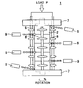
As shown in FIG. 3 and FIG. 4, a voltage
non-linear resistor unit 1 is set so as to be supported by
using a supporting base 7 and a supporting rod 8 in a state
of contacting to the voltage non-linear resistor 2 at a
portion different from a joint surface between the voltage
non-linear resistors 2 and between the voltage non-linear
resistor 2 and the terminal metal fitting 4. Then, a local
portion of the joint portion, on which a soldering material
3 is arranged, is heated by abutting a heat source 9
thereagainst to apply a load to the joint portion in the
vertical direction while giving a rotation. In this case, a
temperature is increased up to the maximum at a temperature
rising .speed of 60°C /min, and then, the maximum temperature
is increased up to 30 °C or more than a melting point of
the soldering material 3 shown in Figure 1. Thereafter, the
temperature is decreased at a temperature rising speed of
1 3
<IMG>
CA 02313914 2000-07-14
thus, the voltage non-linear resistor unit 1 can be
obtained.
It was confirmed that the voltage non-linear
resistor unit 1 thus obtained has the same electrical
characteristic as that in the case where five voltage
non-linear resistors 2 are laminated via an insulator as in
the conventional structure. In the above description, in
the case of manufacturing the voltage non-linear resistor
2, a surface roughness of the sintered body 5 has been
controlled by a grindstone. The surface roughness of the
sintered body 5 may be subjected to a blasting working by
using a powder having a predetermined grain size after
being polished. In such a case, more uniform control can be
performed.
Moreover, in the case where a porosity of the
surface of the sintered body 5 is 15~ or less, a strength
of the base element is improved, and then, de-granulation
is not caused in the grindstone polishing and blasting
working, and therefore, it is possible to obtain a
preferable bonding strength between the base element
surface and the electrode film surface when forming an
electrode film. In addition to these controls, there are
further controls of a temperature rising speed in sintering
and a retaining time, a compound ratio of binder and the
like. It is the most effective to select a composition
ratio for forming the voltage non-linear resistor 2.
1 4
CA 02313914 2000-07-14
More specifically, a composition ratio for forming
the voltage non-linear resistor 2 is selected in the
following manner. That is, Zn0 is used as a main component,
bismuth, cobalt, manganese, antimony and nickel are reduced
to Bia O, Coa 03 , Sba Oa and NiO, respectively, and then,
Bi2 09, is contained by 0. 1 to 5mol~, Co2 Oa is contained by
0.1 to 5mol~, Mn0 is contained by 0.1 to 5mol~, Sba03 is
contained by 0.1 to 5mol~, and Ni0 is contained by 0.1 to
5mol$, respectively, and thus, a fundamental component is
prepared. Boron is contained in BaOa by 0.001 to lwt~, and
aluminum is reduced to A1$' and is contained by 0.05mo1$
with respect to the fundamental component. A sintered body
is manufactured on the basis of a composition ratio
comprising a ratio of Mn0/Sbz03 ranging from 0.3 to 1 and a
ratio of Sb2 03 /Hia 03 ranging from 1 to 7.
The sintered body thus manufactured can reduce its
porosity and improve the strength of base element.
Therefore, the base element is hard to cause a
de-granulation in the grindstone polishing and blasting
working, and it is possible to obtain a preferable bonding
strength between the surface on which, the electrode film
is formed and the electrode film surface.
The voltage non-linear resistor 2 may be formed as
shown in FIG. 5, in place of the voltage non-linear
resistor 2 shown in FIG. 2. More specifically, an inorganic
insulating coating material 10 consisting mainly of a low
1 5
CA 02313914 2000-07-14
melting point glass is applied and baked onto a side of the
sintered body 5, and then, both sides of the sintered body
are polished at a predetermined surface roughness so as
to form an electrode film surface. Subsequently, a Cu
electrode film 11 is formed by an arc spraying method by
using an arc discharge in place of the silver paste 6, and
thus, a voltage non-linear resistor 2 is obtained.
The voltage non-linear resistor 2 thus obtained is
excellent in an insulating characteristic in discharge by
the inorganic insulating coating material 10 applied onto
the side of the sintered body 5, and thus, its withstand
current rating is improved. Moreover, the Cu electrode film
11 is excellent in a conductivity and a heat radiation is
suppressed in its discharge, so that a thermal stress given
to the soldering material 3 can be suppressed.
In this case, the Cu electrode film 11 has been
formed by using an arc spraying method in place of the
silver paste 6. Further, even if the Cu electrode film 11
is formed in the following methods, the same effect could
be obtained. That is, the methods include: a plasma
spraying method of using a Cu alloy, e.g., a Cu-Zn ahoy as
an electrode film material, melting the material by a
plasma heat source so that an electrode film is formed on
the surface of a base element; a high velocity gas flame
spraying method of spraying a material melted by using a
high velocity gas flame to the surface of the base element
1 6
CA 02313914 2000-07-14
at a high velocity so as to form an electrode film; and a
high velocity spraying method of spraying a material at a
high velocity so that an electrode film is formed on the
surface of a base element.
Further, a voltage non-linear resistor 2 as shown
in FIG. 6 may be formed so as to improve the discharge
withstand current rating characteristic and the bonding
strength. More specifically, mullite is used as a main
component of a side insulating coating material, and then,
is baked at 400 °C after adding a predetermined amount of
primary aluminum phosphate, TiOa or FeaOa thereto. Further,
the sintered body 5 is formed with a high resistance layer
12 containing A1P0, using mullite as a main component of 0
to 20wt$, and Ti02 or Fez03 of 0.2 to 5wt$, at the side
thereof. Further, as occasion demands, a non-crystal high
resistance layer 15 using SiOa and A1Z03 as a main
component is further formed on the high resistance layer
12.
On the other hand, the sintered body 5 is polished
at a predetermined surface roughness, and then, an A1 or A1
alloy layer is formed on the polished surface as a first
electrode film 13, and further, a Cu or Cu alloy layer is
formed on the polished surface as a second electrode film
14, and in this manner, the voltage non-linear resistor 2
is obtained.
Further, since an inorganic coating material of the
1 7
CA 02313914 2000-07-14
high resistance layer 12 is used as the side insulating
coating material, the boding strength with the sintered
body 5 can be improved. Moreover, since the porosity of the
side insulating coating material decreases, it is possible
to provide the voltage non-linear resistor 2 which is
excellent in the discharge withstand current rating.
Further, in the case where the high resistance layer 15 is
formed, it is possible to provide the voltage non-linear
resistor 2 which can improve a water repellence and is
excellent in a moisture resistance characteristic.
Moreover, aluminum or aluminum alloy having a low
melting point and a low Young's modulus is used as the
first electrode film 13, and then, is interposed between
layers comprising Cu or Cu alloy which is the second
electrode film 14. Therefore, it is possible to provide a
voltage non-linear resistor 2 which has a more stable
bonding strength.
In the above description, the bonding strength and
discharge withstand current rating characteristics have
been improved by using the voltage non-linear resistor 2
including a material for forming the electrode film and the
insulating coating material. In addition, the state of
forming the electrode film and the thickness of the
electrode film give an influence to the discharge withstand
current rating characteristic. Therefore, the voltage
non-linear resistor unit including the electrode film
1 8
CA 02313914 2000-07-14
having different thickness was previously manufactured by
the voltage non-linear resistor 2 shown in FIG. 2, and
then, a relationship with its discharge withstand current
rating characteristic was investigated.
FIG. 7 is a graph showing a relationship between
the thickness of the electrode film and the discharge
withstand current rating in this embodiment of the present
invention. In the graph, the abscissa takes a thickness of
electrode film, and the ordinate takes a current value
before breakage when energizing an impulse current, which
is plotted. As is evident from FIG. 7, when the thickness
of the electrode film exceeds 300 ~ m, the discharge
withstand current rating characteristic is greatly reduced.
In the above example, the voltage non-linear resistor 2
shown in FIG. 2 has been used. It was confirmed that the
same effect can be obtained as in the case where the
voltage non-linear resistor 2 shown in FIG. 5 and FIG. 6 is
used.
Next, in order to investigate the bonding strength
of the voltage non-linear resistor unit 1, a tensile
strength test was carried out. More specifically, a jig is
attached to a tap provided on the terminal metal fitting 4,
and then, a tensile strength was measured. As a comparative
example (conventional example), a voltage non-linear
resistor unit 1 was prepared in the manner of using a
conductive paste comprising a silver powder, a glass powder
1 9
CA 02313914 2000-07-14
and a binder as a conductive material and then joining the
voltage non-linear resistor 2. 4n the other hand, in the
present invention, a voltage non-linear resistor unit 1 was
prepared in the manner of using the voltage non-linear
resistor 2 shown in FIG. 2 (silver paste + solder), the
voltage non-linear resistor 2 shown in FIG. 5 (Cu +
solder), and the voltage non-linear resistor 2 shown in
FIG. 6 (A1 + Cu/Zn + solder), and thereafter, a comparative
test was performed.
FIG. 8 shows the comparative test result. In FIG.
8, a mark ~ shows a mean value, and a vertical straight
line shows a dispersion. As is evident from FIG. 8, in the
conventional example using a conductive paste comprising a
silver powder, a glass powder and a binder as a conductive
material, the bonding strength was about 0.5MPa. On the
contrary, in the present invention, the bonding strength of
the voltage non-linear resistor unit 1 was about 1.OMPa in
the case of using the silver paste to the voltage
non-linear resistor 2, about 1.2MPa in the case where the
Cu electrode film is formed, and 1.4MPa or more in the case
where A1 sprayed film/Cu-Zn sprayed film was formed, and
thus, a higher bonding strength could be obtained.
Therefore, it can be seen that a preferable characteristic
was obtained.
In the above example, the voltage non-linear
resistor unit 1 has been obtained by using the supporting
2 0
CA 02313914 2000-07-14
base 7 and the supporting rod 8 as shown in FIG. 3 and FIG.
4. The discharge withstand current rating characteristic
greatly varies depending on differences in manufacturing
method, shape of terminal metal fitting, form of joined
state or the like. More specifically, when joining the
voltage non-linear resistor 2, in the case of using no jig
such as the supporting base 7 and the supporting rod 8, a
shift is caused in the joint portion between the voltage
non-linear resistors 2 and in the joint portion between the
voltage non-linear resistor 2 and the terminal metal
fitting 4. As a result, the discharge withstand current
rating characteristic is reduced. Accordingly, the
relationship between the shift in the joint portion and the
discharge withstand current rating characteristic was
investigated.
FIG. 9 is a graph showing a relationship between
the shift between the voltage non-linear resistors 2 and
the discharge withstand current rating. The discharge
withstand current rating test was performed in a manner
that the voltage non-linear resistors 2 were joined to each
other without using the jig such as the supporting base 7
and the supporting rod 8, and the terminal metal fitting 4
was not joined. A larger diameter of the voltage non-linear
resistors 2 was set as R1 and a smaller diameter thereof
was set as R2, and further, the abscissa takes (R1-R2)/R2,
and the ordinate takes a current value before breakage when
2 1
CA 02313914 2000-07-14
energizing an impulse current, which is plotted. As is
evident from FIG. 9, when the value of (R1-R2)/R2 exceeds a
value of 0.05, the discharge withstand current rating is
greatly reduced.
FIG. 10 is a graph showing a relationship between
the positions of the terminal metal fitting 4 and the
voltage non-linear resistor 2 and the discharge withstand
current rating. In FIG. 10, the discharge withstand current
rating test was performed in a manner that the voltage
non-linear resistor 2 was fixed by setting the jig such as
the supporting base 7 and the supporting rod 8 as shown in
FIG. 3 and FIG. 4, and the joint portion of the terminal
metal fitting 4 was joined without setting the jig. A
diameter of the terminal metal fitting 4 was set as R3, a
diameter of the joint surface of the voltage non-linear
resistor 2 was set as R4, and further, the abscissa takes
(R3-R4)/R4, and the ordinate takes a current value before
breakage when energizing an impulse current, which is
plotted. As is evident from FIG. 10, in the case where the
diameter of the terminal metal fitting 4 is larger than
that of the voltage non-linear resistor 2, the discharge
withstand current rating characteristic is greatly reduced.
Moreover, when the value of (R3-R4)/R4 exceeds a value of
0.3, the discharge withstand current rating characteristic
is greatly reduced.
FIG. 11 is a graph showing a relationship between. a
2 2
CA 02313914 2000-07-14
shift from the central portion of the joint portion of the
voltage non-linear resistor and the discharge withstand
current rating. In FIG. 11, a smaller diameter of one joint
surface of the voltage non-linear resistor was set as R5,
and the abscissa takes a difference in a shift between the
central axis of one joint surface and the central axis of
the other joint surface, and further, the ordinate takes a
current value before the breakage when energizing an
impulse current, which is plotted. As is evident from FIG.
11, in the case where the difference in the shift between
the joint portions is larger than a value of 0.1 x R5, the
discharge withstand current rating characteristic was
greatly reduced.
Next, the following factors will be considered as
an influence given to the discharge withstand current
rating characteristic of the voltage non-linear resistor 1.
More specifically, the factors include the shift in the
joint portion and the shape of the terminal metal fitting 4
and the manufacturing conditions as well as the shape of
the voltage non-linear resistor 2 itself. Accordingly, the
relationship between the shape of the voltage non-linear
resistor 2 and the discharge withstand current rating was
investigated.
FIG. 12 is a graph showing a relationship between
the shape of the voltage non-linear resistor 2 and the
discharge withstand current rating. In FIG. 12, a diameter
2 3
CA 02313914 2000-07-14
of the central portion of the voltage non-linear resistor 2
in a thickness direction was set as R6, and a diameter of
the end portion thereof was set as R7, and then, the ratio
of R7/R7 was measured. Thereafter, the voltage non-linear
resistor unit 1 was manufactured by using the jig such as
the supporting base 7 and the supporting rod 8, and then,
the discharge withstand current rating test was carried out
with respect to the voltage non-linear resistor unit 1
thus manufactured. In FIG. 12; the abscissa takes a ratio
R6/R7, and the ordinate takes a current value before
breakage when energizing an impulse current, which is
plotted. As is evident from FIG. 12, when the ratio R6/R7
exceeds a range of 0.9 5 R6/R7 5 1, the discharge
withstand current rating characteristic was greatly reduced.
Moreover, not only the shape of the side of the
voltage non-linear resistor 2 but also a parallelism of
both the end faces thereof has a close relation to the
discharge withstand current rating characteristic. Thus,
the relationship between the parallelism of the voltage
non-linear resistor 2 and the discharge withstand current
rating was investigated. FIG. 13 is a graph showing a
relationship between the parallelism of the voltage
non-linear resistor 2 and the discharge withstand current
rating. As is evident from FIG. 13, if the parallelism
exceeds a value of 20/100, the discharge withstand current
rating characteristic was greatly reduced.
2 4
CA 02313914 2000-07-14
Next, the following is a description on a voltage
nonlinear resistor 2 in the case of using the specific
soldering material 3. In general, an Sn-Pb based eutectic
solder is used as the soldering material. It is preferable
in term of prevention of environmental pollution to use a
solder having a little content of Pb as the soldering
material 3. Therefore, by using the soldering material 3
having a content of Pb by O.lwt% or less and a melting
point of 210°C or more, it is possible to provide the
voltage non-linear resistor unit 1 which is excellent in
the prevention of the environmental pollution.
Namely, there is used a soldering material in which
Sn is used as a main component, and at least one of Cu, Ag
and Sb is contained, and further, the soldering material
consists of a low melting point metallic portion having a
range such that Sn is 70 to 99$, Ag is 3 to 20~ and Cu and
Sb are 5~ or less. The soldering material 3 is specially
excellent in Young's modulus and a tensile strength, and
the voltage non-linear resistor unit 1 using the soldering
material has a stable bonding strength under a high
temperature environment.
In order to compare a difference in a bonding
strength at a temperature of 120°C between the voltage
non-linear resistor unit 1 using the soldering material 3
and the voltage non-linear resistor unit 1 using a Sn
60~-Pb 40~ conventional soldering material which is a
2 5
CA 02313914 2000-07-14
general low melting point metal, a test was carried out
together with a comparative example. As shown in the
following Table 1, 16 (sixteen) soldering materials 3
including the comparative example were prepared, and then,
the bonding strength test was performed with respect to the
voltage non-linear resistor unit 1. In the Table 1, a mark
* shows the comparative example.
[Table 1)
Unit wt% at=120°C
No Sn Cu A' Sb Pb ~ Bonding stren~h
. ~~
1 96:99 3.0 0 0 0.01 0.88
2 98.0 0 0 2.0 0 0.85
3 90:0 0 10.0 0 0 0.
87
_
4* 94.0 6.0 0 0 0 _
0.4
5* 94.0 0 0 6.0 0 0.41
6* 69.0 0 31.0 0 0 0.45
88.5 4.0 3.5 4.0 0 0.88
8* 87.0 6.0 3.0 4.0 0 0.4
9* 65.0 2.0 31.0 2.0 0 0.4
10* 83.0 3.0 4.0 10.0 0 0.4
11 94.0 2.0 4.0 0 0 0.86
12 93.0 4.0 0 3.0 0 0.85
13 88.0 0 10 2.0 0 0.86
14* 67.0 2.0 31.0 0 0 0.41
15* 91.0 6.0 0 3.0 0 0.42
16* 96.0 0 1.0 3.0 0 0.45
In this case, in the above test, each of the
soldering materials 3 shown in the Table 1 was formed into
a disc-shaped foil, and then, was interposed between the
voltage non-linear resistor 2 shown in FIG. 6 and .the
terminal metal fitting 4. Thereafter, a flux was applied
thereto, and a jig such as the supporting base 7 and the
supporting rod 8 shown in FIG. 3 and FIG. 4 was used. Then,
the voltage non-linear resistor unit 1 was heated under a
2 6
CA 02313914 2000-07-14
predetermined condition, and thus, was manufactured. More
specifically, the jig was attached to a tap provided in the
terminal metal fitting 4, and then, the tensile strength
was measured in a state that the voltage non-linear
resistor unit 1 thus manufactured was inserted into a
thermostatic oven at 120°C . The above test result was shown
in the Table 1.
As is evident from the above Table 1, the voltage
non-linear resistor unit 1 consisting of Pb of 0.1$ or
less, Ag of 3 to 20$ or Cu and Sb of 5$, and the remainder
of Sn, has a bonding strength of 0.85MPa under a high
temperature and is excellent in a strength characteristic.
Therefore, it is possible to provide a voltage non-linear
resistor unit 1 which is excellent in a stability.
In the above description, the voltage non-linear
resistor 2 has been joined by applying a flux to the
electrode film forming surface with the use of a low
melting point metal foil as the soldering material 3. It is
also possible to use a paste-like soldering material which
is made by integrating a low melting point metal with a
flux. It is preferable that the paste-like soldering
material consists of a flux portion using a spherical low
melting point metal portion having a diameter of 60 a m or
less and zinc chloride as a main component. In the case of
using the paste-like soldering material, a working
efficiency can be improved.
2 7
CA 02313914 2000-07-14
FIG. 14 is a graph showing a relationship between a
diameter and a bonding strength of a low melting point
metal contained in the paste-like soldering material. As is
evident from FIG. 14, in the case where a diameter of the
low melting point metal portion is 60 a m or more, a flux
is previously volatile, and a wettability becomes worse,
resulting in a reduced bonding strength.
FIG. 15 is a graph showing a relationship between a
thickness and a bonding strength of a low melting point
metal contained in the paste-like soldering material. In
FIG. 15, there is shown a relationship between the
thickness of the low melting point metal and the discharge
withstand current rating characteristic when the paste-like
solder was applied to the voltage non-linear resistor 2,
and then, the voltage non-linear resistors 2 were joined
under a predetermined condition. As is evident from FTG.
15, when the thickness of the low melting point metal
exceeds a value of 300 m, the discharge withstand current
rating characteristic was greatly reduced.
FIG. 16 is a graph showing a relationship between
an applying condition of the paste-like soldering material
and a discharge withstand current rating. In FIG. 16, a
slanted portion shows a region where the discharge
withstand current rating characteristic is 100kA or more.
As shown in FIG. 16, the paste-like soldering material
occupies an area of 60 to 90~ of the joint surface of the
2 8
CA 02313914 2000-07-14
voltage non-linear resistors 2 and is formed so as to
provide an applied thickness of 0.2 to lmm. Further, the
following applying condition is set such that in a range
from 60 to 70~ of an area of the joined surface, an applied
thickness is situated above a straight line connecting the
terminations, and in a range from 80 to 90~ thereof, the
applied thickness is situated below the straight line
connecting the terminations, and thereby, it is possible to
control a thickness of the low melting point metal, after
joined to 300 a m.
By applying the paste-like solder under the
applying condition of the slanted portion shown in FIG. 16,
it is possible to provide the voltage non-linear resistor 2
which is excellent in the discharge withstand current
rating characteristic. Moreover, when joining the voltage
non-linear resistors 2, a heat source is abutted against
the joined surface while a load being vertically applied
thereto, which is effective means for improving the bonding
strength.
FIG. 17 is a graph showing a relationship between a
compression load and a bonding strength when manufacturing
a voltage non-linear resistor unit 1. In FIG. 17, the
abscissa takes a pressing force in joining, and the
ordinate takes a bonding strength. As is evident from FIG.
17, if the pressing force in the joining is 5kgf or more,
the voltage non-linear resistor unit 1 has a high bonding
2 9
CA 02313914 2000-07-14
strength of 1.OMPa. Therefore, it is possible to provide
an excellent Zn0 device unit. This is because the voltage
non-linear resistor unit 1 is heated while a load in
joining being applied thereto so as to reduce a pore of the
solder.
Moreover, the shape of the soldering material after
being joined gives an influence to the bonding strength.
That is, the soldering material 3 is entirely spread to the
joint outer peripheral surface between the voltage
non-linear resistor 2 and the terminal metal fitting 4, and
then, must be continuously and smoothly formed so as to
provide a circular arc-shape from the side of the terminal
metal fitting 4 to the joint surface of the voltage
non-linear resistor 2. In order to form the shape as
described above, when joining the soldering material 3, the
heat source is abutted against a local portion of the joint
portion while rotating voltage non-linear resistor 2.
Hy giving a heat collectively to the local portion
of the joint portion by the heat source, the heat is not
ridded by the voltage non-linear resistor 2, and therefore,
the soldering material 3 can be effectively melted. At the
time of being rotated, the heat can be transferred to the
joint portion, and it is possible to continuously and
smoothly form the soldering material in shape of a circular
arc. In this case, since the joint is carried out while
applying a load, the effect can be further obtained.
3 0
CA 02313914 2000-07-14
In this case, a generated heat is locally
controlled by employing an induction heating method by
arranging a coil around the terminal metal fitting 4 as the
heat source 9, and using a high frequency current, a beam
collection heating method of using a heat source such as a
halogen lamp or the like, a burner heat method of using a
burner, and a heat fan using an electric heating wire.
Next, the above heating conditions will be
described below. By using the heat source mentioned above,
it is possible to make fast a temperature rising speed. If
the temperature rising speed is slow, a flux is previously
volatile, and therefore, it is impossible to sufficiently
wet the low melting point metal and the base material. FIG.
18 shows a relationship between the temperature rising
speed and the bonding strength. As is evident from FIG.
18, in the case where the temperature rising speed is 10 °C
/min or less, the bonding strength is greatly reduced.
The following is a description on an influence
given by a material quality of the terminal metal fitting 4
and the shape thereof to the voltage non-linear resistor 2.
It is desirable that the terminal metal fitting 4 is made
of steel, copper and copper alloy. The bonding strength was
investigated with respect to a voltage non-linear resistor
unit 1 formed by using these materials and a voltage
non-linear resistor unit 1 formed by using an aluminum
material as a comparative example. In the above test, a jig
3 1
CA 02313914 2000-07-14
was attached to a tap provided in the terminal metal
fitting 4, and then, a tensile strength was measured. The
test result is as shown in the following Table 2. In the
Table 2, a mark * shows a comparative example.
[Table 2]
Material quality of terminal metal Strength(MPa)
f ittin _ _
1* aluminum allo AA2011 0.45
2 steel material 1.10
3 co er JIS C1020 1.05
4 co er allo JIS C5212 I.12
brass JIS C2680) 1.15
As is evident from the above result, when joining
the terminal metal fitting 4 using steel, copper and copper
alloy, the bonding strength is l.OMPa or more, and
therefore, it is possible to provide a Zn0 device unit
which is excellent in the bonding strength. Moreover, it
was confirmed that the same effects as those mentioned
before can be obtained by the materials other than the
those in the' examples 2 to 5 shown in the Table 2, that is,
steel, copper and a copper alloy.
In the examples 2 to 5, in the case where the
terminal metal fitting 4 was made of an aluminum material,
the bonding strength was greatly reduced. The terminal
metal fitting 4 was subjected to a plating treatment, and
thereby, it is possible to improve the bonding strength.
That is, the terminal metal fitting 4 made of aluminum or
an aluminum alloy was subjected to Ni, Sn or Zn plating,
3 2
CA 02313914 2000-07-14
and thereafter, a voltage non-linear resistor unit 1 was
manufactured. The bonding strength test was carried out
with respect to the voltage non-linear resistor unit 1 thus
manufactured in the same manner as in the above-described
examples 2 to 5. The test result is shown in the following
Table 3.
[Table 3]
Base material: Aluminum (AA1050)
No. Platin material Stren th MPa
1 Ni ~ 1.05
2 Sn 1.12
3 Zn 1. 05 - _
As is evident from the above-described result,
since the terminal metal fitting 4 is subjected to Ni, Sn
or Zn plating, the bonding strength is 1.OMPa or more, and
therefore, it is possible to provide a Zn0 device unit
which is excellent in a bonding strength. Moreover, it was
confirmed that the same effect can be obtained in the
materials other than the examples 1 to 3 shown in the Table
3, that is, aluminum, an aluminum alloy steel, copper or a
copper alloy.
The following is a description on an influence to
the voltage non-linear resistor 2 given by a shape of the
terminal metal fitting 4. That is, the terminal metal
fitting 4 has a structure, in accordance with the shape of
the voltage non-linear resistor 2, that the joint surface
is formed like a disc, and then, the central portion on the
3 3
CA 02313914 2000-07-14
side opposite to the joint surface is formed with a
projected screw portion having a diameter of 1/3 of or more
than the terminal metal fitting 4 of the jointed portion,
and thus, the terminal metal fitting 4 is applied to the
voltage non-linear resistor unit 1. Accordingly, it is
possible to manufacture an arrester unit having a second
terminal metal fitting described later fixed the terminal
metal fitting 4 by a screw. In this case, the diameter of
the projected screw portion has been set to 1/3 or more of
the terminal metal fitting of the joint portion. The reason
is because of preventing a deformation in the case where a
load is applied in a transverse direction.
An influence to the bonding strength given by the
maximum thickness of the terminal metal fitting 4 from the
joint surface of the voltage non-linear resistor 2 was
investigated. That is, a plurality of voltage non-linear
resistor units 1 having different thicknesses of mounting
portions were manufactured, and then, a tensile strength
test was performed. In the test, a jig was attached to a
tap provided in the terminal metal fitting 4, and then, a
tensile strength was measured. The result is shown in FIG.
19.
In FIG. 19, the abscissa takes the minimum
thickness of the terminal metal fitting, and the ordinate
takes a bonding strength. As is evident from the result,
the minimum thickness of the joint portion of the terminal
3 4
CA 02313914 2000-07-14
metal fitting 4 is set to 2mm or more, and the bonding
strength becomes 1.OMPa or more. Therefore, it is possible
to provide a Zn0 device unit which is excellent in the
bonding strength.
In the terminal metal fitting 4, since the
surrounding of the joint surface is subjected to
C-finishing or R-finishing, the surrounding of the joint
surface is formed with a groove so that the soldering
material 3 is easy to be stored. Thus, the soldering
material 3 is uniformly spread around the terminal metal
fitting 4. It is therefore possible to provide a voltage
non-linear resistor unit 1 which has a stable bonding
strength. A bonding strength was investigated with respect
to the voltage non-linear resistor unit 1 using the
terminal metal fitting 4 whose surrounding of the joint
surface is subjected to C-finishing or R-finishing. The
result is shown in the following Table 4.
[Table 4]
No. Kind of .terminal finishing Stren th
1 C-finishin (0.5mm) 1.23
_
2 R-finishing (0.5mm) 1.25
As is evident from the above-described result,
since the surrounding of the joint surface of the terminal
metal fitting 4 is subjected to the C-finishing or
R-finishing, the bonding strength becomes 1.OMPa or more.
Therefore, it is possible to provide a voltage non-linear
resistor unit which is excellent in the stable bonding
3 5
CA 02313914 2000-07-14
strength, whereby it becomes possible to securely join the
voltage non-linear resistor 2 and to provide a voltage
non-linear resistor unit 1 which can contribute to a
compact size of transformer equipment.
Hereunder, another embodiment of the present
invention relating an arrester unit utilizing the voltage
non-linear resistor mentioned herein before.
FIG. 20 is a cross sectional view showing an
arrester unit 16 according to one embodiment of the present
invention. The arrester unit 16 is applicable to a column
arrester, a distribution arrester, an arrester for
transmission line and the like. As shown in FIG. 20, the
arrester unit 16 is composed of a voltage non-linear
resistor unit 1, a perforated insulative tube 17 covering
the voltage non-linear resistor unit 1, a metallic disc 18
having a through hole, a second terminal metal fitting 19
attached to the terminal metal fitting 4 of the voltage
non-linear resistor unit l, and an elastic insulating
cover member 20 covering the components other than the
second terminal metal fitting 19.
The voltage non-linear resistor unit 1 manufactured
in any one of the above-described embodiments is used. The
voltage non-linear resistor unit 1 is covered with a
thermosetting perforated insulating tube 17, and then, the
metallic disc 18 is inserted into the projected screw
portion of the terminal metal fitting 4 on both the end
3 6
CA 02313914 2000-07-14
sides of the voltage non-linear resistor unit 1, and
thereafter, the second terminal fitting 19 is fixed by
means of screw so that the perforated insulating tube is
held therebetween. Then, the unit thus assembled is put in
a baking furnace, and then, is thermally hardened at a
temperature of 200°C or less. Subsequently, the unit is set
in a mold having a predetermined shape and is covered by
the elastic insulating covering member 20. Then, the unit
is thermally hardened at a temperature of 200 °C or less,
and thus, the arrester unit 16 can be obtained.
In this case, the metallic disc 18 includes a
plurality of convex protrusions at a side facing the
voltage non-linear resistor unit 1, and the perforated
insulating tube 17 can be firmly held. Moreover, in the
case of arranging a plurality of the arrester units 16 in
series, as shown in FIG. 21, the second terminal metal
fitting 19 including a screw portion 21 at its both sides
is used. More specifically, the second terminal metal
fitting 19 can be engaged with the terminal metal fitting 4
of the voltage non-linear resistor unit 1 by means of screw
and includes the screw portion 21 which is cylindrically
extended and has a concave portion at the center of the
upper portion so as to directly combine the arrester unit
16 in series.
Moreover, since the side portion of the second
terminal metal fitting 19 is set to an arithmetic average
3 7
CA 02313914 2000-07-14
surface roughness (central line average surface roughness)
of 100 m or more, the second terminal metal fitting 19 is
preferably engaged with the elastic insulating cover member
20. Therefore, the elastic insulating cover member 20 is
not peeled off even if it receives an external force, an
ambient temperature and an internal heating effect. As a
result, it is possible to prevent an insulative function
from being reduced by sucking a moisture due to the peeling.
In the arrester unit 16, the voltage non-linear
resistor unit 1 is covered with the thermosetting
perforated insulating tube 17. This serves to prevent each
component of the arrester from being scattered in the case
where the arrester is broken by an excessive surge coming
therethrough. Moreover, when an internal pressure rises up
by an excessive surge coming therethrough, the internal
pressure is uniformly dispersed, and it is possible to
prevent a stress from being concentrated in breakage.
As shown in FIG. 22 and FIG. 23, the elastic
insulating cover member 20 is formed with a thin wall
portion 22 at one side. As shown in FIG. 22, the elastic
insulating cover member 20 is formed with a slit-like thin
wall portion 22 in a vertical direction, and as shown in
FIG. 23, the elastic insulating cover member 20 is formed
with a circular-shaped thin wall portion in a vertical
direction. The thin wall portion 22 is formed so as to
control an arc discharge to one direction.
3 8
CA 02313914 2000-07-14
Further, it is to be noted that the present
invention is not limited to the described embodiments and
many other changes and modifications may be made without
departing from the scopes of the appended claims.
3 9