Note: Descriptions are shown in the official language in which they were submitted.
CA 02314049 2000-07-19
METHOD FOR FORMING AN ELECTRICAL CONDUCTIVE PATTERN ON A
SUBSTRATE
This application claims the benefit of US Provisional Application Serial
Number
601096,233 that was filed on Aug. 12, 1998 and is co-pending herewith.
BACKGROUND OF THE INVENTION
The present invention was also described in a paper dated 1210111997, that was
submitted by the inventors and accepted into the Disclosure Document program
as
Disclosure Document No. 434368 on 04/07/1998.
FIELD OF THE INVENTION
With regard to the classification of art, this invention is believed to be
found in the
general class entitled Electrical Conductors and Insulation and more
particularly to those
subclasses pertaining to methods for forming an electrical conductive pattern
on a
carrier material. The electrical conductive patterns are used in electrical
circuit boards,
low profile heater elements, and connecting means for electronic devices.
DESCRIPTION OF RELATED ART
The art of forming a conductive pattern on a substrate and the resulting
products
are well known. Traditionally the conductive pattern is formed on a copper
clad substrate
by employing a subtractive process, such as etching, machining and the like;
or an
additive process such as printing and the like. It has been found that there
is a need to
produce circuit patterns that are precise while minimizing the gaps between
the circuit
paths. The minimizing of the gaps between the circuit paths and the problems
associated therewith have been identified in US patent No. 5,493,074 that
issued to
Murata et al on 02120/1996. Murata teaches the use of a subtractive process
such as
Docket No. 98029 1
CA 02314049 2000-07-19
etching for producing the conductive pattern then subsequently filling the
gaps between
the circuits with a cured product. However this process is slow, capital
intensive, and
involves the use of chemicals that may be hazardous to the environment. The
known
subtractive and/or additive processes mentioned above do not provide the
electrical
conductive pattern that has the precision and repeatability that is needed for
certain
applications. The lack of precision and repeatability results in variations of
conductor
values such as conductance, resistance and the like.
SUMMARY OF THE INVENTION
The present invention solves the above identified needs by precisely
separating
the conductive electrical paths by mechanical means. The instant invention
does not
require the use of hazardous chemicals. The present invention therefore
provides a
method that is economical by increasing productivity while minimizing the cost
for the
disposal of waste. The present invention lends itself to automatic production
machinery.
The present invention may be briefly summarized with respect to its objects.
It is
an object of this invention to provide and it does provide a method for
producing an
electrical conductive pattern on a substrate that results in a precisely
formed conductive
circuit while simultaneously maintaining the separation of the conductive
paths.
It is a further object of this invention to provide and it does provide a
method for
producing an electrical conductive pattern on a flexible substrate that is
arrayed for
attachment to a support means.
It is another object of this invention to provide and it does provide a method
for
producing an electrical conductive pattern on a substrate that results in an
induction
heater that has a low profile and provides a routing of a cun-ent through a
conductive
Docket No. 98029
CA 02314049 2000-07-19
pathway that produces heat when a selected electrical current is applied. This
method
provides a precisely sized conductive pathway that is consistently
reproducible.
It is still another object of this invention to provide and it does provide a
method
for producing a precise electrical conductive pattern on a flexible substrate
that results in
an induction heater that has a low profile and is arrayed for attachment to an
article that
is to be heated
One embodiment of the method of the present invention may be briefly described
as a method for producing an electrical conductive pattern on a substrate
including the
steps of:
a) providing a substrate layer, the substrate layer being non conductive and
having a predetermined thickness;
b) bonding a layer of a conductive material to one face of the substrate layer
by
means of heat and pressure to activate a first bonding means, the first
bonding means
having a predetermined melting temperature, the one face of the substrate
layer being
cleaned and prepared by a treating means prior to the application of the
bonding means;
c) bonding a cover layer to an exposed surface of the conductive material by
means of heat and pressure to activate a second bonding means, the cover layer
having
a predetermined thickness and fully covering the exposed surface of the
conductive
material, the second bonding means having a predetermined melting temperature;
d) forming at least one path for an electrical circuit in the conductive
material by
severing the conductive material by and with a blade, the blade inGuding a
predetermined cutting edge configuration, the blade being further arrayed for
providing a
predetermined cutting pattern, the blade may also include a temperature
control means
Docket No. 98029 3
CA 02314049 2000-07-19
for maintaining the blade within a predetermined temperature range; the
cutting edge
configuration of the blade being arrayed for severing the cover layer and
penetrating a
selected distance into the substrate layer during the severing of the
conductive material,
the blade simultaneously shaping and setting selected portions of the top
layer, the
second bonding means, the conductive material, and the first bonding means so
that at
least one continuous predetermined gap is provided between severed portions of
the
conductive layer;
e) subsequently applying an insulating coating completely over an exposed
surface of the severed top layer so that the insulating coating also fills all
of the
predetermined gaps;
f) allowing the insulating coating to set so that the insulating coating
maintains the
predetermined gap as and when the flow of current passes through the at least
one
path;
g) applying, attaching, and connecting electrical connection terminals into
selected positions along the at least one path;
h) selectively applying a pressure sensitive strip to an exposed surface of
the
insulating surface;
i) selectively applying a pressure sensitive strip to a second face of the
substrate;
and
j) dividing the substrate and the circuits carried thereon into discreet
units.
In addition to the above summary, the following disclosure is intended to be
detailed to insure adequacy and aid in the understanding of the invention.
However, this
disclosure, showing particular embodiments of the invention, is not intended
to describe
Docket No. 98029
CA 02314049 2000-07-19
each new inventive concept that may arise. These specific embodiments have
been
chosen to show at least one preferred or best mode of the present invention as
presently known. These specific embodiments, as shown in the accompanying
drawings, may also include diagrammatic symbols for the purpose of
illustration and
understanding.
BRIEF DESCRIPTION OF THE DRAWING
FIG. 1 represents a schematic of a first automated embodiment of the method of
the present invention.
Fig. 2 represents a schematic of a second automated embodiment of the method
of the present invention. This view showing a first portion of the second
automated
embodiment.
Fig. 3 represents a finishing portion of the second automated embodiment of
the
method of the present invention.
Fig. 4 represents a plan view of a typical article that may be produced by the
method of the present invention.
Fig. 5 represents a fragmentary cross sectional view of the article of Fig 4
prior to
the forming of the conductive paths therein.
Fig. 6 represents a fragmentary cross sectional view of the article of Fig 4
after
the forming of the conductive paths therein.
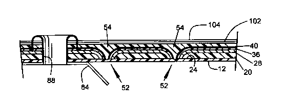
Fig. 7 represents a fragmentary cross sectional view of the article of Fig 4.
This
view showing one of the embodiments of a finished article.
In the following description and in the appended claims, various details are
identified by specific names for convenience. These names are intended to be
generic in
Docket No. 98029
CA 02314049 2000-07-19
their application while differentiating between the various details. The
corresponding
reference numbers refer to like members throughout the several figures of the
drawing.
The drawings accompanying and forming a part of this specification disclose
specific details for the sole purpose of explanation. It is to be understood
that the
specific details may be modified without departing from the concept and
principles of the
invention as claimed. This invention may be incorporated into methods other
than those
that are specifically shown.
DETAILED DESCRIPTION OF THE INVENTION
Referring to the drawings which will be used to schematically describe a
sequence or series of the steps that are included in the method of the present
invention.
This sequence of steps is preferably carried out on an in-line continuously
moving
conveyor type of apparatus that transports an elongated substrate and layers
bonded
thereto in the direction of the an-ows by means of drive rollers 11. However
the process
also lends itself to an indexing type of apparatus that is capable of feeding
either
1 b elongated webs or individual substrate pieces that have elongated layers
bonded
thereto.
Referring in particular to Fig. 1, Fig 5; and Fig. 6, a first embodiment of
the
present invention is generally identified as a manufacturing process 10. This
process 10
starts with a substrate or base material 12, shown as a coil of material 14,
that is
unwound, in the direction of the arrow, from an unwind stand or mandrel 16 by
conventional means, such as a nip roll and dancer combination 18, but not
limited
thereto. The substrate 12 is preferably selected from non conductive materials
such as
linear polymers, cross-linked polymers, spun silica, mica, fiberglass, and the
like. The
type of substrate used is dependent on the end use for the article to be
manufactured.
Docket No. 98029 6
CA 02314049 2000-07-19
More specific, but non-limiting, examples of material will be disclosed in
connection with
the several examples described below. A blanket coating of a bonding means 20
is
applied to the substrate 12 by an applicator means 22. It is preferred that a
top face 24
of the substrate 12 be treated by a surface treating means 26, such as a
corona
discharge but not limited thereto, for leaning the top face 24, prior to the
application of
the bonding means 20.
A layer of a conductive or conductor material 28, such as aluminum, gold,
copper
and the like, but not limited thereto, is bonded to the substrate 12 and
bonding means
20 laminate, by application of heat and pressure. The heat and pressure is
applied
thereto by a second pair of nip rollers 30. The heat and pressure should be
sufficient to
activate the bonding means 20 while providing a secure bond. Preferably, the
conductive material 28 is fed from a supply coil 32. The supply coil 32 may be
supported
by and with conventional means such as a cradle arrangement 34, as shown in
Fig. 1, or
alternatively by other suitable means, such as a mandrel. The thickness of the
conductor
material 28 is dependent on the desired electrical characteristics of the type
of conductor
material 28 and may be selected from within the range of 0.08 mm (0.0003 in)
and 1.6
mm (0.0625 in.).
A second bonding means 36 is applied to an exposed surface of the conductor 28
and the substrate 12 bonded assembly at an applicator station 38. Subsequently
a non
conductive cover layer 40 is bonded to the conductive material 28 by the
application of
heat and pressure by a third pair of nip rollers 42. Of course, the heat and
pressure
should be sufficient to activate the second bonding means 36 while providing a
secure
bond. The non conductive cover layer 40 is preferably fed from a supply roll
44. The
Docket No. 98029
CA 02314049 2000-07-19
supply roll 44 may be supported by and with a conventional means such as
either a
cradle arrangement 34, as shown, or by a mandrel similar to 16.
At least one continuous conductive pattern or path 46 and at least one
remaining
portion 48 is formed in the conductive material 28 by a combination of a
rotary cutting
tool or blade 50 and anvil 51. An example of the conductive path 46 may be
more clearly
seen in Fig. 4 and Fig. 6. The cutting tool or blade 50 should be contoured,
sharpened,
and adjusted to sever the cover layer 40, the inductive material 28, and
penetrate a
selected distance, in the neighborhood of 0.025 mm (0.001 in.), into the
substrate or
base layer 12. During the severing action by the tool 50, the severed edges of
the
conductive path 46 and the severed edges of the remaining portion are
displaced
downward to form a shaped gap 52 therebetween. The blade 50 sets the shape of
the
gap 52 for filling during the subsequent steps in the process. It has been
found that a
blade 50 should have a maximum draft angle of its side wall 53 of less than
7.5 degrees
with respect to vertical to provide the desired results.
It is preferred that the cutting tool 50 be arrayed to include a temperature
control
means TC, seen in Fig. 1, for maintaining its temperature within a
predetermined range.
The temperature control means TC would heat or cool the tool 50, as needed, to
maintain a selected temperature range. It is preferred that the selected
temperature
range allow the setting of the shape of the gap 52 while simultaneously
stabilizing the
cutting tool dimensions. The stabilization of the cutting tool dimensions
provides
predictable and repeatable conductive patterns or paths 46.
The cover layer 40 should be of a sufficient thickness to ensure a clean
severing
of the conductive material by the blade 50 while subsequently holding the
desired shape
of the gap 52. It has been found that a thickness between the range of 0.0088
mm
Docket No. 98029 g
CA 02314049 2000-07-19
(0.00035 in.) and 0.13 mm (0.005 in) is sufficient for the process as
presently practiced.
More specific examples will be discussed in connection with the several
examples
described below.
Referring now to Fig. 1 and Fig. 7, an electrical insulating coating 54 is
applied to
the cover layer 40 by a coating assembly 55 so that the coating 54 flows into
the gaps
50 and completely fills them while simultaneously covering the cover layer 40.
The
insulating coating 54, such as varnish, cross-linked polymer and the like
needs to be
subsequently set by being dried or cured, so that the gap 50 is maintained
between the
conductive path 46 and the remaining portion 48. The insulating layer 54 may
be
formulated for including adhesive properties for attaching to a supporting
article.
Referring again to Fig. 1 and Fig. 4, subsequent to the application of the
insulating coating 54, the substrate 12 carrying the conductive pattern
thereon may be
severed into discrete portions 56 by a cutting means 58. The cutting means 58
may be
carried on a reciprocating carriage, not shown, that travels with substrate
12. The timing
and positioning of the cut with respect to the pattern of the conductive path
is preferably
controlled by an eye or registration mark 60 that was previously imprinted on
the
substrate and detected by a sensing means 62, such as photocell. One non
limiting
example of the imprinting an eye mark 60 may occur prior to the placement of
the
conductive material 28 by a printing means 64. Alternatively, the eye mark 60
may be
imprinted on a selected surface the conductive material 28 .The printing of
the eye mark
60 by the printing head 64 may be in response to a signal or pulse from the
machine
control system. The discrete portions 56 may be delivered to other stations
for testing
and/or for the application of electrical connectors. The embodiment 10
described above
Docket No. 98029 g
CA 02314049 2000-07-19
may be used when the article or discrete portions 56 have a rectilinear
peripheral outline
66, as shown in dashed outline in Fig. 4.
Referring now to Figures 2, 3, 5, 6, and 7; a first stage 68 of a second
embodiment for the execution of the method of the present invention is
generally
identified as 70. In this second embodiment 70, the sequence of steps is
similar to the
first embodiment 10. This process 10 also starts with a substrate or base
material 12,
shown as a coil of material 14, that is unwound, in the direction of the
arrovy A, from an
unwind stand or mandrel 16 by a non-limiting conventional means, such as a nip
roll and
dancer combination 18. A blanket coating of a bonding means 20 is applied by
an
applicator means 22 to the substrate 12 that has been previously treated, as
describe in
connection with embodiment 10. It is to noted that the bonding means 20 may
have
been previously applied to the substrate 12 at a step prior to being wound as
coil 14.
A layer of a conductive or conductor material 28, such as aluminum, gold,
copper
and the like, but not limited thereto, is bonded to the substrate 12 and
bonding means
20 laminate, by application of suitable amount heat and pressure by nip rolls
30 to effect
a good bond. As mentioned above, the flexible conductive material or foil 28
is fed from
a supply coil 32.
A second bonding means 36 is applied to an exposed surface of the conductor 28
and the substrate 12 bonded assembly at an applicator station 38. Subsequently
a non
conductive cover layer 40 is bonded to the conductive material by the
application of the
appropriate amount of heat and .pressure by a third pair of nip rollers 42.
The non
conductive cover layer 40 is preferably fed from a supply roll 44.
At least one continuous conductive pattern or path 46 and at least one
remaining
portion 48 is formed in the conductive material 28 by a rotary cutting tool or
blade 50 and
Docket No. 98029 10
CA 02314049 2000-07-19
anvil 51. One non limiting example of a conductive path 46 and its cross
section shape
may be more clearly seen in Fig. 4 and Fig. 6. The action of the rotary
cutting tool 50
was described above in connection with embodiment 10.
It is preferred that an eye mark and article identifying means 60 be placed on
the
substrate 12 by a printing means 64 for subsequent use. The positioning of the
eye
mark and its control have been discussed above.
Referring in particular to Fig. 2 and Fig. 7, an electrical insulating coating
54 is
applied to the cover layer 40 by a coating assembly 55 so that the coating 54
flows into
the gaps 52 and completely fills them while simultaneously covering the cover
layer 40.
The insulating coating 54, that has been also described above, needs to be
subsequently set by being dried or cured, so that the gap 52 is maintained
between the
conductive path 46 and the remaining portion 48.
The distinguishing difference between embodiments 10 and 70 is that the
elongated laminated article containing the conductive pattern 46 thereon is
fed by drive
rollers 11 onto a conventional winding means 72 to be formed into a coil 74
for finishing
of the process at a separate stage 80 of the press 70.
Referring now to Figures 3, 4 and 7, the second or finishing stage 80 of the
process 70 begins with the coil 74 of the elongated laminated web being
supported on a
mandrel 82 of a machine unwind stand. The insulating coating 54 surtace of the
laminate has been wound on the outside of the coil 74 at the end the first
stage 68 of the
process 70, that was previously described in connection with Fig. 2. The web
of the
elongated flexible laminate is fed in the direction of the arrow A.
Docket No. 98029 11
CA 02314049 2000-07-19
Electrical terminals 84 are automatically applied to the elongated laminate by
a
terminal application means 86. This terminal application means 86 includes the
operation of punching an aperture 88, more clearly seen in Fig. 7, in the
laminate then
automatically depositing a terminal 84 into the aperture 88, subsequently the
terminal 84
is fastened to the elongated laminate by a riveting process. The positioning
and
placement of the electrical terminal 84 or alternatively another selected
electrical
component is controlled by a sensing means 62, such as a photocell, that
senses the
relative position of the eye mark 60 that was previously applied in the first
stage 68.
It is preferred that, the attachment of the terminals 84 to the conductive
path or
paths 46 be tested at a testing station 90. The testing station may include
means for
identifying any particular circuits that do not meet testing standards by
printing
appropriate indicia thereon.
A finished product 92 that has a shaped periphery 94, seen more clearly in
Fig. 4
is separated from the elongated web of laminated material by a reciprocating
cutting tool
assembly 96. The tool 96 is arrayed for clamping the laminate and travels
therewith
during the cutting operation. A sequencing means may separate the accepted
artiGes 92
from the rejected artiGes 92 by a transverse shuttle means, not shown.
Alternatively, the
cutting tool assembly 96 may be operated by a sequencing program to only
separate
good circuits from the elongated web. The remaining elongated web of material
may be
wound onto a coil 98 by a rewind assembly 100 for recycling purposes.
In some applications, such as in the production of a low profile induction
heater, it
may be desirable to apply a pressure sensitive adhesive strip 102 to a
selected side of
the elongated web of the laminated product prior to the application of the
electrical
terminals 84. The pressure sensitive adhesive strip 102 preferably has a
protective
Docket No. 98029 12
CA 02314049 2000-07-19
covering 104 that is removed when the discrete articles 92 are applied to a
surface of an
article to be heated. Another benefit found when using the article 92 as an
induction
heater is in its use as a heater for a glass surface, such as a glass
defogger, aquarium
heater and the like. The remaining portion 48 aids in the uniform distribution
of the heat
through a rigid insulating material, such as glass. The periphery 94 of the
article 92 may
be contoured to closely match any surface to which it may be attached.
In the previous discussion, the second embodiment 70 has been depicted as
being broken into two separate stages 68 and 80. It is to be noted that method
of the
second embodiment 70 may be carried out in one continuous series of steps on a
single
production apparatus.
FIRST EXAMPLE
A first non-limiting example of materials that may be used in the production
of the
discrete articles or portions 56 or 92 that are to be used in a low
temperature application
includes: a substrate 12 made from a polypropylene material that has a
thickness
between 0.08 mm (0.003 in) and 0.8 mm (0.030 in.); a conductive material 28 of
copper;
a cover layer 40 of 0.04 mm (0.0015 in) thick polyester. The laminate is
bonded together
by a first bonding means 20 and second bonding means 36 such as a hot melt
adhesive
having a melt temperature of 110 degrees C (230 F). The insulating coating 54
is a
solvent based varnish.
SECOND EXAMPLE
A second non-limiting example of materials that may be used in the production
of
the discrete articles or portions 56 or 92 that are to be used as a low
profile induction
heater having a maximum temperature range of 148.9 degrees C (300 F) includes:
a
substrate 12 made from a polyester material that has a thickness between 0.08
mm
Docket No. 98029 13
CA 02314049 2000-07-19
(0.003 in) and 0.8 mm (0.030 in.); a conductive material 28, such as aluminum
and
having a thickness between 0.08 mm. and 0.126 mm.; a cover layer 40 of 0.04 mm
(0.0015 in) thick polyester. The laminate is bonded together by a first
bonding means 20
and second bonding means 36 such as a hot melt adhesive having a melt
temperature
of 182.2 degrees C. (360 F). The insulating coating 54 is preferably a cross
linked
polymer. Alternatively the insulating coating 54 may include adhesive
properties for
adhering to an article to be heated. The predetermined electrical and or
heating
characteristics and the width of the path 46 of the conductive material 28
will determine
the thickness needed.
THIRD EXAMPLE
A second non-limiting example of materials that may be used in the production
of
the discrete articles or portions 56 or 92 that are to be used in a low
profile induction
heater having a maximum temperature range of 171 degrees C (340 F) includes: a
substrate 12 made from a polyimide material that has a thickness between 0.08
mm
(0.003 in) and 0.8 mm (0.030 in.); a conductive material 28 of aluminum having
a
thickness between 0.08 mm. and 0.126 mm.; a cover layer 40 of 0.04 mm (0..0015
in)
thick polyester. The laminate is bonded together by a first bonding means 20
and
second bonding means 36 such as a resin based adhesive having a melt
temperature of
232.2 degrees C. (450 F). The insulating coating 54 is a high temp varnish.
As it was previously mentioned, that the method of the present invention may
be
carried out by using the embodiments disclosed as the first embodiment 10 and
the
second embodiment 70. The second embodiment 70 may be carried out either in a
single or multiple stages. This method also lends itself to the production of
electrical
circuits on individual pieces of a substrate material. The steps of the
process may be
Docket No. 98029 14
CA 02314049 2000-07-19
performed manually, semi-automatically, or on an indexing type of apparatus.
It is to be
noted that the cutting tool 50 has been preferably shown as being of a rotary
type,
however a planar cutting tool may also be used in its place. The planar
cutting tool may
be employed in a manual or semi-automatic operation.
The discxete articles 92 made using a flexible substrate 12 may be bonded to a
support board by means of a pressure sensitive adhesive or strip.
The method of the present invention may also be employed for producing back to
back circuit patterns on the flexible substrate 12. One non-limiting example
for producing
circuit patterns on each side of the flexible substrate employs a continuous
process
similar to that shown in Fig. 1 wherein subsequent to the step of applying the
insulating
coating 54 by the coating assembly 55, the laminate passes through a
conventional
turnover bar so that the top face 24 of the substrate is now facing downward.
The
process or the steps described in conjunction with Fig. 1 is repeated prior to
the
selective application of terminals, finishing andlor cutting of the laminate
into discrete
articles. It is to be noted that a two stage process similar to process 70 may
be
employed. A selectively different type andlor thickness of conductive material
28 may be
applied to each side of the substrate for the back to back circuits.
The present invention provides a method of reproducing circuit patterns that
are
dimensionally uniform, and may be produced automatically at economical rates.
The
method of the first embodiment 10 produces little or no waste. The method of
the
alternate embodiment 70 produces minimal waste.
It is to be noted that the second nip rollers 30 and the third nip rollers 42
may
need to have a temperature control system and means similar to temperature
control
Docket No. 98029 15
CA 02314049 2000-07-19
means TC, similar to that depicted in Fig. 1 in connection with tool 50. It is
preferred that
nip rollers 30 and 42 includes an adjustable pressure means.
Directional terms such as °front", "back", °in", "out",
"downward", "upper", "lower,
°vertical" and the like may have been used in the description. These
terms are
applicable to the embodiments shown and described in conjunction with the
drawings.
These terms are merely used for the purpose of description in connection with
the
drawings and do not necessarily apply to the position in which the present
invention may
be used.
While these particular embodiments of the present invention have been shown
and described, it is to be understood that the invention is not limited
thereto and
protection is sought to the broadest extent that the prior art allows.
What is claimed is:
Docket No. 98029 16