Note: Descriptions are shown in the official language in which they were submitted.
CA 02314213 2000-07-19
Eh 363 CA
Device for Measuring the Material Level in a Vessel
FIELD OF THE INVENTION
The present invention relates to an apparatus for determining the material
level in
a vessel. In particular, the present invention relates to a material level
measurement
apparatus which includes a signal generating unit, a coupling unit, a
conductive element
and a receiving/evaluation unit.
BACKGROUND OF THE INVENTION
A material level in a vessel is measured by means of measuring systems that
measure different physical quantities. These quantities are then used to
derive the desired
information regarding the material level. In addition to mechanical sensors,
capacitive,
conductive and hydrostatic measuring sensors, and sensors operating on the
basis of
ultrasonic, microwaves or other electromagnetic radiation can be used to
measure material
level.
Many applications, for example, in the petrochemical, chemical and food
industries, require highly accurate measurements of the level of liquids or
bulk materials
in vessels (tanks, silos, etc.). Increasingly, sensors are used in which short
high frequency
electromagnetic pulses or continuous microwaves are coupled to a conductive
cable
sensor and by means of this cable sensor are introduced into the vessel in
which the
material is stored. This cable sensor can be any type of conductive element.
Physically, this measuring method utilizes the effect occurring at the
interface
between two different media, e.g. air and oil or air and water. A portion of
the guided
high frequency pulses or the guided microwaves is reflected at the media
interface due to
the abrupt change (discontinuity) of the dielectric constants of the two
media. The
reflected portion is returned via the conductive element to a receiving
device. The
reflected portion is greater for greater differences between the dielectric
constants of the
two media. The distance to the interface can then be calculated from the
propagation time
of the reflected portion of the high frequency pulses or microwaves. Knowing
the empty
distance of the vessel permits calculation of the material level within the
vessel.
CA 02314213 2000-07-19
Eh 363 CA
Sensors with guided high frequency signals (pulses or waves) are distinguished
by
significantly lower attenuation compared to sensors that freely emit high-
frequency pulses
or waves (free-field microwave systems (FMR) or >true radar systems=). The
reason is
that the energy flow is highly concentrated along the cable sensor or the
conductive
element. Furthermore, sensors with guided high frequency signals provide
higher
measurement quality at close range than freely emitting sensors.
A further advantage of sensors with guided high frequency signals is the
superior
safety and reliability of the level measurement. This is due to the fact that
measurement
with guided measuring signals is largely independent of the product
characteristics of the
material (moisture, dielectric constant, material change), the vessel design
(materials,
geometry) or other operating conditions (dust, deposits and reflection angle).
SUMMARY OF THE INVENTION
An objective of the present invention is to provide a sensor apparatus with a
conductive element in which the conductive element of the sensor does not come
into
direct contact with the material being measured.
The present invention attains this objective in the following manner. A signal
generating unit generates high frequency measuring signals. A coupling unit
couples
these measuring signals to a conductive element, the length of the conductive
element
corresponding at least to the maximum level of the vessel. The conductive
element is
disposed at a predetermined distance to the material in a vessel, the distance
being such
that the electromagnetic field produced by the measuring signals interacts
with the
material and is partially reflected when it meets the surface of the material
in the vessel.
The time characteristic of the reflected echo signals guided along the
conductive element
are detected by the receiving/evaluation unit and analyzed.
An alternative embodiment of the present invention provides that the
conductive
element is disposed outside the vessel. In this case, the vessel itself must
be made of a
non-conductive material at least within a defined sphere of influence of the
conductive
element. Materials that are typically used are plastics or glass.
The arrangement of the level measuring device outside the vessel has of course
a
number of obvious advantages. In addition to ensuring simple installation, the
2
CA 02314213 2000-07-19
Eh 363 CA
arrangement of the measuring device outside the material being measured
prevents
contamination or, in case of an aggressive material, corrosion of the
conductive element.
This makes it possible to use inexpensive materials to manufacture the
conductive
element. Costly encapsulation of the electrical parts of the measuring device
may be
largely eliminated.
In another embodiment of the present invention, the vessel, or at least a
portion of
the vessel within the sphere of influence of the electromagnetic field, is
structured as a
viewing glass which does not interfere with the electromagnetic field, and
which can be
transparent in the visible part of the spectrum. If the material level is
measured directly
on a vessel designed as a viewing glass, the invention can also include a
conductive shield
as an additional element. The shield is located on the opposite side of the
viewing glass
from the conductive element to ensure that interfering radiation is
effectively shielded.
In another embodiment of the present invention, the conductive element is
mounted directly on the vessel or the viewing glass by a simple connection.
This
connection is preferably an adhesive bond in which the conductive element is
glued to the
outside wall of the vessel or the viewing glass.
Furthermore, a protective shield made of an electrically conductive material
is
provided either in combination with the above embodiment or alone. The
protective
shield is positioned such that the conductive element is disposed between the
vessel and
the protective shield. The protective shield and the conductive element are
spatially
separate from each other. Preferably, a dielectric material is arranged
between the
protective shield and the conductive element. In the simplest case, this
dielectric material
is air. The protective shield can furthermore be constructed in such a way
that it almost
completely encloses the conductive element on the side facing away from the
vessel. The
purpose of the protective shield is to provide protection from interfering
radiation from
the space lying behind the conductive element, which can negatively affect the
measuring
accuracy of the level measurements.
The conductive element itself can have any shape as viewed in cross-section.
It
can for instance be circular, semi-circular or polygonal. It is preferable
that the
conductive element be made of at least two conductors, whereby at least one of
the two
conductors is connected to ground. Improved measuring results are achieved
particularly
3
CA 02314213 2000-07-19
Eh 363 CA
in the case where the conductive element is mounted outside the vessel and is
moreover
shielded from interfering radiation from the exterior by a protective shield.
The reason is
that in a multi-part embodiment of the conductive element, the electromagnetic
field
extending into the vessel is less strongly influenced by the protective
shield.
While the above-described embodiments of the present invention describe the
arrangement of the conductive element on the outside of the vessel, an
alternative
embodiment described below relates to an arrangement of the conductive element
inside
the vessel. In particular, a dielectric sheath or sleeve surrounds the
conductive element at
least in the area up to the maximum level of material in the vessel.
Furthermore, the
distance of the conductive element from the material to be detected is
dimensioned in
such a way that the measuring signal interacts with the material and is
partially reflected
when it strikes the surface of the material.
A desired distance between the conductive element and the material may be
realized either through the selection of the thickness of the dielectric
material and/or
through the distance of the material from the conductive element located
within the
dielectric material. Furthermore, the conductive element may be disposed
inside a sleeve
made of a non-conductive material. The sleeve is placed inside the vessel and
the
conductive element is subsequently introduced into the sleeve. However, the
conductive
element and the sleeve may also be designed as a single unit that is then
introduced into
the vessel. For example, the conductive element may be surrounded directly by
the non-
conductive material.
BRIEF DESCRIPTION OF THE DRAWINGS
The invention will be explained in detail by means of the following drawings:
Fig. 1 shows a longitudinal section of a first embodiment of the present
invention;
Fig. 2 shows a cross-section of a second embodiment of the present invention;
Fig. 3 shows a cross-section of a third embodiment of the present invention;
Figs. 4A-4D show a cross-section of a several different types of conductive
elements that may be used in connection with the present invention;
Fig. 5 shows a longitudinal section of a fourth embodiment of the present
invention; and
4
CA 02314213 2000-07-19
Eh 363 CA
Fig. 6 shows a block diagram of a signal generating unit and a receiving/
evaluation unit.
DETAILED DESCRIPTION OF PREFERRED EMBODIMENTS
S OF THE INVENTION
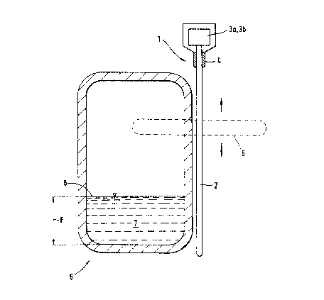
Fig. 1 shows a longitudinal section of a first embodiment of the present
invention.
The level measuring device 1 comprises a signal generating unit 3a, a coupling
unit 4, a
conductive element 2 and a receiving/evaluation unit 3b. Measuring signals
generated in
the signal generating unit 3a are coupled via the coupling unit 4 and guided
along the
conductive element 2. The conductive element 2 is mounted outside a vessel 6
by means
of any type of connection, the connection not being specifically depicted in
the drawing.
A direct connection between the vessel 6 and the conductive element 2 is not
required
since the electromagnetic field 5 accompanying the measuring signals along
their path
covers a relatively large area in space. The vessel 6, at least in the main
sphere of
influence of the electromagnetic field 5, is made of a non-conductive material
(e.g. glass,
plastic, etc.).
As briefly described above, the measuring signals guided along the conductive
element 2 produce an electromagnetic field 5 in the surrounding space. The
electromagnetic field 5 is coaxially aligned and moves parallel to the
longitudinal axis of
the conductive element 2. Due to the abrupt change of the dielectric constants
at the
junction between the media, for example, air and material 7, the
electromagnetic field 5 is
partially reflected as soon as it comes into contact with the surface 8 of the
material 7.
The echo signals returned along the conductive element 2 are received in the
receiving/evaluation unit 3b. The propagation time of the measuring/echo
signals permits
calculation of the distance traveled. Knowing the distance between the
coupling unit 4
and the floor of the vessel 6 makes it possible to determine the level of
material 7 in the
vessel 6.
Fig. 2 shows a cross-section of a second embodiment of the present invention.
Material 7, the level of which is being measured, is located inside a viewing
glass 9. The
viewing glass 9 is transparent to the electromagnetic field, and it can also
be transparent
to the visible spectrum. The conductive element 2 is disposed outside the
viewing glass
5
CA 02314213 2000-07-19
Eh 363 CA
9. To reduce the influence of interfering radiation on the measuring results,
a curved
protective shield 10 made of a conductive material is positioned along the
conductive
element 2 and the viewing glass 9. The protective shield 10 is connected to
ground and
provides effective shielding from interfering radiation.
Fig. 3 shows a cross-section of a third embodiment of the present invention.
The
conductive element 2 is disposed on the side of the vessel 6. A curved
protective shield
11 is provided to shield interfering radiation from the environment. The
protective shield
11 has a semi-circular cross-section and its side edges extend to the
immediate proximity
of vessel 6. A dielectric material 12 is provided between the interior surface
of the
protective shield 11 and the conductive element 2. The protective shield 11 is
mounted
outside vessel 6 by means of any type of connection, the connection not being
specifically
depicted in the drawing. In the case shown, the conductive element 2 comprises
two
conductors 29, 30, with conductor 30 connected to ground. As described above,
the
double or multiple division of the conductive element 2 has a positive effect
on the
electromagnetic measuring field. Particularly when the protective shield 11 is
used for
protection against interfering radiation from the environment, the attenuation
of the
electromagnetic field in the interior of the vessel 6 is reduced.
Fig. 4 shows the cross-sections of several different types of conductive
elements 2
that may be used in the present invention. In Fig. 4A, the conductive elements
2 is
polygonal (e.g. rectangular) in shape. In Fig. 4B, the conductive elements 2
is semi-
circular in shape. In Fig. 4C, a pair of conductive elements 2 is shown, one
being circular
and the second being rectangular in shape. Fig. 4D shows a type of mounting of
the
conductive element 2 on the vessel 6. The rectangular conductive element 2 is
glued to
the outer vessel wall by means of an adhesive bond 14.
Fig. 5 shows a longitudinal section through a fourth embodiment of the present
invention. In contrast to Figs. 1 B 4 which show the conductive element 2
mounted
outside the vessel 6, Fig. 5 shows an arrangement of the conductive element 2
within the
vessel 6. The conductive element 2 is inserted into a dielectric sleeve 15.
The sleeve 15
is made, for example, of glass. In Fig. 5, an additional dielectric medium in
the form of
air is located between the conductive element 2 and the sleeve 15. However,
the
conductive element may also be sheathed by dielectric material to isolate it
from material
6
CA 02314213 2000-07-19
Eh 363 CA
7. Furthermore, the conductive element 2 and the sleeve 15 may be formed
either as
separate components or as a single unit.
Fig. 6 shows a block diagram of the signal generating unit 3a and the
receiving/evaluation unit 3b. The signal generating unit 3a includes a
transmission clock
generator 17 and a transmission pulse generator 18. The transmission clock
generator 17
generates a transmission clock signal which is supplied to the transmission
pulse
generator 18 which generates a measuring signal. Preferably, the transmission
pulse
generator 18 produces electromagnetic measuring signals in the form of short
low energy
high frequency pulses. Such transmission pulse generators, as well as
electronic circuits
and receiving/evaluation units used in connection therewith, are described,
for example,
in U.S. Patent 5,609,059.
The measuring signals are supplied to the conductive element 2 via the
coupling
unit 4. In reverse direction, reflected echo signals reach the
receiving/evaluation unit 3b
via the conductive element 2, the coupling unit 4, a directional coupler 19,
and a high pass
filter 20.
The receiving/evaluation unit 3b includes a time delay circuit 21, the input
of
which is connected to the transmission clock generator 17 for receiving the
transmission
clock signal. The time delay circuit 21 produces a sampling clock signal that
corresponds
to the transmission clock signal delayed by a variable delay time. The
variable delay time
is provided, for example, by means of a sawtooth generator. The sampling clock
signal is
supplied to a sampling pulse generator 22, which generates sampling pulses as
a function
of the sampling clock signal and supplies them to a first input of a sample-
and-hold
circuit 23. Transmission pulse and sampling pulse generators 18, 22 are
preferably
identical such that the signals they generate are distinguished only by the
variable delay
time. The reflected echo signals are supplied to a second input of the sample-
and-hold
circuit 23 via the directional coupler 19 and high pass filter 20. EP 0 875
772 describes in
detail a receiving and evaluation unit that is very well suited for the
present invention.
In operation, short transmission pulses are produced, preferably periodically
with
the transmission clock frequency. The reflected echo signals are supplied to
the sample
and-hold circuit 23 in which a sampling pulse is superimposed on each echo
signal and
the resulting total signal is detected. The total signal is amplified by an
amplifier 24,
7
CA 02314213 2000-07-19
Eh 363 CA
digitized by an analog-to-digital converter 25 that is arranged in series with
the amplifier
24, and supplied as a sampling value to a microprocessor 26.
The total signal is a measure for the alignment of the echo signal and the
sampling
pulse. The echo signals arrive periodically, whereby successive sampling
pulses are
distinguished from each other by a time delay determined by the sawtooth
function.
Provided that successive echo signals do not differ significantly, the
sampling-and-hold
circuit 23 supplies a stroboscopic recording of the echo signals. This is
normally the case
since, in practice, the level of material does not change significantly in the
time between
successive transmission pulses.
The microprocessor 26 is connected via a first line 27 to the transmission
clock
generator 17 and the transmission pulse generator 18 and via a second line 28
to the time
delay circuit 21 and the sampling pulse generator 22. In operation,
microprocessor 26
initiates regular measuring cycles. During a measuring cycle, the
electromagnetic
measuring signals are periodically produced, as described above, and the
reflected echo
signals are sampled. A measuring cycle ends when a complete cycle of the time
delays
provided by the time delay circuit 21, for example by a cycle of a sawtooth
function, has
been completed. The individual sampling values are each recorded in
conjunction with
the assigned time delay. The propagation time is then determined using the
recorded
sampling values.
8