Note: Descriptions are shown in the official language in which they were submitted.
CA 02315177 2000-06-14
WO OOI25961 PC'T/US98/23545
1
COMPONENT OF PRINTED CIRCUIT BOARDS
Field of the Invention
The present invention relates generally to printed circuits, and more
particularly, to components used in the manufacturing of printed circuit
boards and
other articles.
Background of the Invention
In the manufacture of printed circuit boards, sheets of copper foil are
typically
bonded to a dielectric layer of a partially cured epoxy resin containing woven
glass
fiber (such a dielectric layer is conventionally referred to as a "pre-preg").
In the
manufacture of copper clad laminates, sheets of copper foil are typically
bonded to
another layer of foil. In both processes, the copper foil is etched to produce
conductive paths. In such processes, it is extremely important to avoid
contamination
of the copper foil sheets in that any foreign matter contacting the copper
foil, such as
resin dust, fiberglass fibers, hair, grease, oil or the like, may result in
dots, dents,
deposits or pits on the copper foil that can adversely affect the formation of
the
conductive paths forming the printed circuits.
Copper foil is conventionally formed by an electrodeposition process.
Following the production of the copper foil, it is known to secure a metallic
substrate
to one side of the copper foil to protect that side of the copper foil from
contamination
during subsequent handling and shipping. The protected side of the copper foil
is
typically the side used to form the conductive pathways, while the exposed
side of the
foil is typically the side that is attached to a pre-preg or bonded to another
layer of
copper foil. The protective metallic substrate remains attached to the copper
foil as it
is attached to the pre-preg or bonded to the other layer of copper foil. The
protective
metallic substrate is subsequently removed and discarded (or recycled) to
expose the
protected, uncontaminated side of the foil for processing to form the
conductive
pathways.
U.S. Patent No. 5,153,050 to Johnston discloses a copper/aluminum/copper
laminate wherein the shiny side of a copper foil is bonded along its
peripheral edges to
an aluminum substrate. U.S. Patent No. 5,674,596 to Johnston further discloses
securing copper foil to a metallic substrate, such as a steel or a stainless
steel substrate.
U.S. Patent No. 5,512,381 to Konicek et al. discloses securing copper foil to
a copper
substrate.
CA 02315177 2000-06-14
WO 00/25961 PCT/US98/23545
2
Each of the foregoing structures uses a relatively expensive material, e.g.,
aluminum, stainless steel and copper, to form the disposable, protective
substrate. In
addition to the cost of such materials, copper and aluminum are relatively
soft metals
that are susceptible to image transfer during lamination of multi-layer
laminates,
particularly at high lamination temperatures and pressures. Stainless steel is
a stronger
metal than copper or aluminum, and possesses the corrosion resistance
necessary to
avoid contamination of the copper foil sheet. As a result, stainless steel
finds
advantageous application at higher laminating temperatures and pressures.
However,
corrosion resistance and higher strength of stainless steel come at a price.
Typically,
stainless steel sheet is even more expensive than copper and aluminum sheet.
The present invention provides a component for manufacturing printed circuit
baards that has a copper foil protected by a metallic substrate, wherein the
metallic
substrate has the corrosion resistance of stainless steel at a significantly
reduced cost.
Summary of the Invention
1S In accordance with the present invention, there is provided a component for
use in manufacturing articles such as printed circuit boards. The component is
comprised of a laminate constructed of a sheet of copper foil that, in a
finished printed
circuit board, constitutes a functional element, and a sheet of carbon steel
having a
layer of an inert metal thereon. The sheet of carbon steel constitutes a
discardable
element. One surface of the copper sheet and the surface of the inert metal
layer on
the carbon steel sheet are essentially uncontaminated and are engageable with
each
other at interfaces. The copper sheet is attached to the inert metal layer of
the carbon
steel sheet at its borders to define substantially uncontaminated central
zones inwardly
of the edges.
In~ accordance with another aspect of the present invention, there is provided
a
sheet of copper foil for manufacturing mufti-layer laminates comprising a
sheet of
copper foil having a thickness greater than about 5 microns. The copper foil
has a first
surface adapted for adhering to a fiber reinforced polymer layer, and a second
surface'
to be exposed after the first surface is adhered to the fiber reinforced
polymer layer. A
protective sheet of carbon steel having a thickness of about 0.05 mm to about
2.0 mm
is provided. The carbon steel sheet has a layer of chromium with about 0.1
grams/m2
to about 10 grams/m2 electrodeposited on its surface. The layer of chromium
engages
CA 02315177 2000-06-14
WO 00/2596r PCT/US98/23545
3
the second surface of the copper sheet and is attached thereto in a manner
defining
substantially uncontaminated central zones.
It is an object of the present invention to provide a component having a
copper
sheet for use in manufacturing articles, such as printed circuit boards, and a
metallic
S substrate to protect a surface of the copper sheet before and during a
manufacturing
process.
It is a further object of the present invention to provide a component as
described above wherein the metallic substrate is a relatively low cost,
discardable
item.
It is a further object of the present invention to provide a component as
described above wherein the metallic substrate is formed of carbon steel and
has an
outer layer of an inert metal thereon far engagement with the copper sheet.
It is a further object of the present invention to provide a component as
described above wherein the inert metal is chromium.
It is another object of the present invention to provide a component as
described above that is suitable for high temperature processing applications.
A still further object of the present invention is to provide a component as
described above wherein the discardable metallic substrate has a coefficient
of thermal
expansion approximately equal 'to the coefficient of thermal expansion of
press plates
used in forming laminated circuit boards.
A still further object of the present invention is to provide a component as
described above wherein the metallic substrate is dimensioned and used as a
press
plate in a circuit board forming operation.
These and other objects will become apparent from the following description
of a preferred embodiment taken together with the accompanying drawings and
the
appended claims.
Brief Description of the Drawings
The invention may take physical form in certain parts and arrangement of~
parts, a preferred embodiment of which will be described in detail in the
specification
and illustrated in the accompanying drawings which form a pari hereof, and
wherein:
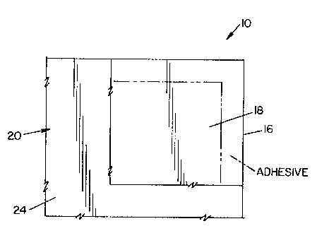
FIG. 1 is an enlarged sectional view of a component used in forming articles
such as printed circuit boards, illustrating a preferred embodiment of the
present
invention; and
CA 02315177 2000-06-14
WO 00/25961 PCT/US98/23545 -
4
FIG. 2 is a partially sectioned, top plan view of a portion of the component
shown in FIG. I.
Detailed Description of Preferred Embodiment
Referring now to the drawings wherein the showing is to illustrate a preferred
~ . .
S embodiment of the invention only, and not for the purpose of limiting same,
FIG. 1
shows a component 10 for use in manufacturing articles such as printed circuit
boards,
illustrating a preferred embodiment of the present invention. In the
embodiment
shown, component 10 is comprised of a metallic substrate, designated 12,
having
copper sheets, designated 20, attached thereto. Substrate 12 is comprised of a
metallic
sheet I4 having thin layers 16 of an inert metal formed on the surfaces
thereof.
In accordance with a preferred embodiment of the present invention, metallic
sheet 14 is comprised of conventional, mild carbon steel. Carbon steel ChPPr ~
a
preferably has a thickness of from about 0.05 mm to about 2.0 mm, and more
preferably, has a thickness of from about O.I mm to about 0.3 mm. Layers 16 of
inert
metal on sheet 14 are preferably selected from the group consisting of nickel,
copper,
cobalt, brass, chromium, antimony, cadmium and combinations thereof. In a
preferred
embodiment of the present invention, layer 16 is comprised of essentially pure
chromium. Chromium layer 1 b preferably has a thickness of from about 0. I
gram/m2
to about 10 grams/mz, and more preferably, has a thickness of from about 2.0
grams/m2 to about 4.0 grams/m2. Chromium layer 16 may be deposited through a
number of various conventionally known techniques, such as wet chemical
deposition,
autocatalytic deposition, chemical vapor deposition, e.g., evaporation or
sputtering,
ion bombardment or electrolytic deposition. In a preferred embodiment of the
present
invention, chromium layer 16 is electrolytically deposited on carbon steel
sheet 14. In
a preferred embodiment, carbon steel sheet 14 has a Rockwell 30-T hardness of
between about 40 and about 60, a tensile strength of between about 390
newtons/mm2
and about 440 newtons/ mm'', a thickness of about 0. I8 mm, and chromium layer
I 6 is
about 2 grams/m2. ,
In accordance with the present invention, carbon steel sheet 14, with the
chromium layers 16 thereon, has a width approximately equal to the width of
copper
sheets 20 to be attached thereto. Surface 22 of copper sheet 20 that is
ultimately to be
exposed and etched into a printed circuit is placed facing surface I8 of
chromium
layer 16 of carbon steel sheet 14. Surface I8 of chromium layer 16 is cleaned
so as to
CA 02315177 2000-06-14
WO 00/25961 PCT/US9$/23545
be substantially contamination-free. Copper foil sheets 20 are attached to
chromium
layer 16 of substrate 12 such that interior portions of the facing surfaces of
sheets 20
are substantially uncontaminated in a region 30 inwardly from edge portions 32
of
sheets 20. More specifically, copper sheets 20 are preferably attached to
substrate 12
5 in the vicinity of edge portions 32 by an adhesive or an adhesive-like
material (not
shown). Such materials may include adhesives, resins or tapes. Copper sheets
20 may
also be adhered by mechanical means, such as crimping, deforming and the like.
In a
preferred embodiment of the present invention, beads of a flexible adhesive
(not
shown), conventionally known in the art, are applied in edge portions 32 of
copper
sheets 20 and substrate 12 to secure the same to each other.
The present invention thus provides a component 10 for forming circuit boards
or other articles that includes a copper sheet 20 adapted to be attached to a
polymer
board. Surface 22 of copper sheet 20 that is to be ultimately exposed and
etched by a
forming process is protected by a relatively inexpensive metallic substrate 12
having a
thin layer 16 of an inert metal on an inner core 14 of carbon steel. The inert
metal
protects surface 22 of copper 20 from corrosion conventionally associated with
ordinary carbon steel. At the same time, the carbon steel core 14 of metallic
substrate
12 provides the strength of steel, at significantly less cost than using
stainless steel
sheet. Importantly, the carbon steel core 14 has essentially the same
coefficient of
thermal expansion as the press plates that conventional, mufti-opening presses
use in
forming printed circuit boards. Thus, the laminated structure to be formed
with copper
sheet 20 is disposed between two materials having the same or similar
coefficients of
thermal expansion, i.e., the press plate and substrate 12. This provides a
more uniform
distribution of stresses in the laminate during the heating and compression
steps of
processing. In addition, the use of chromium as a protection layer on the
steel allows
for higher processing temperatures when using polymer materials requiring
higher
setting temperatures.
The foregoing description discloses preferred embodiments of the present .
invention. It should be appreciated that the embodiments are described for the
purpose of illustration only, and that numerous alterations and modifications
may be
practiced by those skilled in the art without departing from the spirit and
scope of the
invention. It is intended that all such modifications and alterations be
included insofar
as they come within the scope of the invention as claimed or the equivalents
thereof.