Note: Descriptions are shown in the official language in which they were submitted.
CA 02315434 2000-07-27
- 1 -
SEMICONDUCTOR DEVICE
BACKGROUND OF THE INVENTION
1. Field of the Invention
The present invention relates to a
semiconductor device, more particularly, to a DRAM gain
cell suitable for embedding with a logic circuit.
2. Description of the Related Art
In recent years, semiconductors have been
becoming increasingly miniaturized. Not only are many
elements embedded on a single chip, but also several
functions have to be incorporated.
As a typical example of this, there is a LSI
embedding both a DRAM and logic circuit.
By embedding not only a logic circuit but also
a memory in an ASIC (application specific integrated
circuit), the range of application of the ASIC is
expanded.
At the present time, in a DRAM (dynamic random
access memory), the most typical type of high density,
high capacity semiconductor memory, as shown in Fig. 10,
a memory cell is configured by connecting a transistor T
controlled in on/off state by the potential of a word
line WL and a memory capacitor MCAP in series between a
bit line BL and common potential line SL.
CA 02315434 2000-07-27
M . i
2 -
In a one-transistor one-capacitor type memory
cell MC, a connection point between the memory capacitor
MCAP and the transistor T forms a storage node ND. The
111" or "0" of data is differentiated by a difference of
the amount of a charge stored in this storage node.
It is necessary to cause a sufficiently large
potential change in the bit line BL in order to secure
stable operation when reading stored data. The capacity
for storage of a charge (capacitance of the capacitor) is
determined for the memory capacitor MCAP from this
viewpoint.
Along with the reduction in the occupied area by
a semiconductor memory cell, however, the capacitance value
of the capacitor itself tends to fall. In addition, the
increases in memory capacity have led to an increase in the
bit line capacitance. Therefore, it is becoming even harder
to obtain a readable bit line potential compared with the
past.
As measures to solve this problem, various
capacitor structures have been proposed such as a stack
type, fin type, cylindrical type, or other stacked capaci-
tor having a capacitor electrode increased in surface area
per unit area and a trench capacitor etc.
However, due to the limits in processing
technology on the aspect ratio of the trench formed on a
CA 02315434 2000-07-27
3 -
substrate, the height of a stacked electrode layer, etc. or
the increase of the number of process steps for forming a
complex structure and the resultant increase in
manufacturing cost etc., it is becoming difficult to
increase the capacitance value of a capacitor per unit
area.
On the other hand, the capacitance of a
capacitor is proportional to the dielectric constant of a
capacitor insulating film sandwiched between electrodes, so
a capacitor insulation material with a high dielectric
constant is also being developed.
In addition to the difficulty of development of
a dielectric material itself, however, there are extensive
development themes such as development of electrode
materials with a good affinity with the dielectric or
development of processing techniques for these new
materials. Also, the development costs or newly introduced
production equipment etc. pose an sizeable burden. As a
result, the DRAM production cost has been continuously
increasing. Therefore, even if the cell area is reduced and
DRAMs are made larger in capacity, it is proving hard to
reduce the cost per bit.
In view of this, when trying to reduce the cell
area without changing the structure and materials, the
reading signal of a DRAM cell becomes smaller, and,
CA 02315434 2000-07-27
4 -
ultimately, it is expected that detecting data stored in
the memory cell will become difficult.
Further, as a DRAM cell, in addition to the one-
transistor one-capacitor type mentioned above, there is
known for example a three-transistor type memory cell not
using a capacitor and using three transistors. In this
case, in addition to the two word lines for writing and
reading, two bit lines for writing and reading besides are
necessary so the number of interconnection layers is
increased.
However, a large number of interconnection
layers may well become a limiting factor in reducing the
cell area.
SUMMARY OF THE INVENTION
The present invention has been made to solve the
above problems and has as its object to provide an
inexpensive memory having a DRAM function. More
particularly, when considering mounting together with a
logic circuit, it is to provide a semiconductor device
minimizing the effect on the logic process and enable
realization of a hybrid circuit of a memory cell and
peripheral circuit easily and at a low cost.
The semiconductor device according to the present
invention comprises a memory cell having a plurality of
CA 02315434 2000-07-27
-
active elements and at least one passive element.
Further, in the present invention, the plurality of
active elements comprising the memory cell are field effect
transistors having three terminals which comprise two
5 diffusion layers forming a source or drain, and a gate or
four terminals which comprise two diffusion layers forming
a source or drain, a gate and a substrate or a layer which
includes an area at which channel is formed, and the
passive element comprising the memory cell is a capacitor
having an insulating layer between a first electrode and a
second electrode.
Further, in the present invention, the active
elements comprising the memory cell include at least a
transistor having a function of writing data and a
transistor having a function of reading data.
Further, in the present invention, the memory cell
comprises two field effect transistors and one capacitor, a
first field effect transistor is an N-channel type or P-
channel type, and a second field effect transistor is also
an N-channel type or P-channel type.
Further, in the present invention, the memory cell is
configured by a second diffusion layer terminal of the
first field effect transistor, the second electrode of the
capacitor, and a gate electrode terminal of the second
field effect transistor connected together and, further,
CA 02315434 2000-07-27
6 -
the first electrode of the capacitor is connected to a word
line, a first diffusion layer terminal of the first field
effect transistor is connected to a bit line, a gate
terminal of the first field effect transistor is connected
to a control gate line, a first diffusion layer terminal of
the second field effect transistor is connected to the bit
line, and a second diffusion layer terminal of the second
field effect transistor is connected to a predetermined
power supply terminal.
Further, in the present invention, at least one of
the first electrode and second electrode of the capacitor
serves also as an interconnection layer.
Further, in the present invention, all of the active
elements comprising the memory cell are N-type field effect
transistors or P-type field effect transistors.
Further, in the present invention, when arranging the
memory cell in an array, the gate electrode terminal of the
first field effect transistor of each of a plurality of
memory cells connected to one word line is connected to one
control gate line.
Further, in the present invention, when arranging the
memory cell in an array, the gate electrode terminal of the
first field effect transistor of each of the plurality of
memory cells connected to one bit line is connected to one
control gate line.
CA 02315434 2000-07-27
7 -
Further, in the present invention, the memory cell is
embedded with a logic circuit.
According to the present invention, the stored charge
of the passive element, for example, capacitor, may be one
of an extent enabling control of the on/off state of an
active element, that is, first field effect transistor
(read transistor), in accordance with the stored data.
Therefore, in this memory cell, since there is no
need for directly charging and discharging a large capacity
bit line by the stored charge of the capacitor such as with
a one-transistor one-capacitor type DRAM, the capacity of
charge storage of the capacitor can be made small.
At a result, in a memory cell of this structure, it
is, not necessary to tinker with the capacitor structure to
increase the amount of charge storage per unit area or to
develop a capacitor dielectric material of a high
dielectric constant. That is, since the structure is not
complex, it is easy to make and further there is no rise in
the production cost along with complication of the process.
Further, since there is one bit line, the cell area
is small, and the degree of integration can be made higher
and since a logic transistor can be used without any major
change, the compatibility with the CMOS logic process is
good and it is possible to mount a DRAM function together
with.a logic circuit by few processes.
CA 02315434 2000-07-27
8 -
BRIEF DESCRIPTION OF THE DRAWINGS
These and other objects and features of the present
invention will become clearer from the following
description of the preferred embodiments given with
reference to the accompanying drawings, in which:
Fig. 1 is a circuit diagram of an embodiment of a
gain cell as a semiconductor device according to the
present invention;
Fig. 2 is a pattern diagram of a memory cell
according to the present embodiment;
Fig. 3A is a sectional view along the line A-A in
Fig. 2, and Fig. 3B is a sectional view along the line B-B
in Fig. 2;
Figs. 4A and 4B are sectional views for explaining
the process of production of a memory cell according to the
present invention;
Figs. 5A and 5B are sectional views for explaining
the process of production of a memory cell according to the
present invention;
Figs. 6A to 6C are plane views for explaining the
process of production of a memory cell according to the
present invention;
Figs. 7A to 7C are plane views for explaining the
process of production of a memory cell according to the
present invention;
CA 02315434 2000-07-27
9 -
Figs. 8A to 8C are plane views for explain the
process of production of a memory cell according to the
present invention;
Fig. 9 is a view of an example of the layout of the
DRAM gain cell according to the present invention; and
Fig. 10 is a circuit diagram of a one-transistor one-
capacitor type DRAM cell.
DESCRIPTION OF THE PREFERRED EMBODIMENTS
Below, preferred embodiments will be described with
reference to the accompanying drawings.
Figure 1 is a circuit diagram of an embodiment of a
gain cell as a semiconductor device according to the
present invention.
This gain cell GMC, as shown in Fig. 1, has a read
transistor TR, write transistor TW, capacitor CAP, bit line
BL, word line WL, and control gate line CGL.
Note that in Fig. 1, TA denotes a first electrode of
the capacitor CAP, TB denotes a second electrode of the
capacitor CAP, WG denotes a gate terminal of the write
transistor TW, WA denotes one source/drain terminal of the
write transistor TW, WB denotes the other source/drain
terminal of the write transistor TW, RG denotes a gate
terminal of a read transistor TR, RA denotes one
source/drain terminal of the read transistor TR, and RB
CA 02315434 2000-07-27
- 10 -
denotes the other source/drain terminal of the read
transistor TR.
For example, m x n (m, n: any natural numbers) number
of cells GMC are arranged in matrix in a memory cell array.
In the case of this array structure, the first
electrodes TA of the capacitors CAP of memory cells
arranged on the same row are connected to a common word
line WL.
Also, the gate terminals WG of the write transistors
TW of memory cells arranged on the same column are
connected to a common control gate line CGL.
Further, one source/drain terminals RA of the read
transistors TR of the memory cells arranged on the same row
are connected to the bit line BL.
Moreover, the bit line BL is connected to, for
example, a not shown latch-type sense amplifier to which a
reference cell is connected.
In this way, the gain cells GMC are used for a memory
cell array, a memory peripheral circuit is added, and the
assembly is embedded with a logic circuit (not shown in
Fig. 1) in an LSI chip.
The write transistor TW and read transistor TR
comprise insulation gate type field effect transistors, for
example, n-channel MOS (NMOS transistors).
In a write transistor TW, the gate terminal WG is
CA 02315434 2000-07-27
- 11 -
connected to the control gate line CGL, one source/drain
terminal WA is connected to the bit line BL, and the other
source/drain terminal WB is connected to the second
electrode TB of the capacitor CAP.
In a read transistor TR, the gate terminal RG is
connected to the second electrode of the capacitor CAP, one
source/drain terminal RA is connected to the bit line BL,
and the other source/drain terminal RB is connected to a
supply line of a reference voltage Vs (ground voltage
GND).
A storage node SN of the memory cell GMC is comprised
by the connection point of the second electrode TB of the
capacitor CAP and the other source/drain terminal WB of the
write transistor TW connected thereto and the gate terminal
RG of the read transistor TR.
In the capacitor CAP, the first electrode TA is con-
nected to the word line WL.
The capacitor CAP does not have to be large in
capacity, so is configured by so-called MIM (metal
insulator metal) type capacitor formed by an insulator
(layer) between two metal interconnections.
For example, the first electrode TA is configured by
the same metal interconnection as the word line WL of
aluminum (Al) etc., while the second electrode is
configured by the metal interconnection for the logic
CA 02315434 2000-07-27
- 12 -
circuit.
The insulator is formed by a nitride film formed by,
for example, plasma CVD (hereinafter referred to as a
plasma nitride film).
Further consider a capacitor CAP having such a
configuration.
The charge stored in the capacitor CAP is mainly lost
by junction leakage. 1 fA is assumed as a typical leak
value.
If the potential difference to be stored is 1V and
the discharge time (data holding time) is 600 ms, the held
charge becomes as follows:
600 ms x 1 fA = 0.6 fC
Further, the capacity of the capacitor CAP becomes as
follows:
0.6 fC/1V = 0.6 fF
If 8F2 (F is a design rule) is assumed as an electrode
area of the capacitor CAP, when F = 0.13 m, 8F2= 0.1352
/.Cm2. If a dielectric of a dielectric constant = 7 is used,
the thickness d of the insulator becomes 14 run as shown
below.
d=(7.8.854e-12.O.1352e-12/(O.6e-15)=14e-9[m]
The above condition can be sufficiently realized if a
plasma nitride film is used as an insulating film.
Also, the capacitor CAP is not a capacitor such as
CA 02315434 2000-07-27
- 13 -
one of a complex general purpose DRAM and may be a
parallel-plate type capacitor.
Further, a plasma nitride film is formed by a low
temperature process enabling it to be used even after Al or
other interconnections are formed, so it is possible to
make an MIM type capacitor making use of an interconnection
layer of a logic circuit as mentioned above.
Next, the pattern and example of the sectional
structure of a memory cell GMC of a single bit line type of
Fig. 1 will be explained with reference to Figs. 2, 3A and
3B.
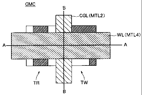
Figure 2 is a pattern diagram of the memory cell GMC
according to the present embodiment, Fig. 3A is a sectional
view along the line A-A in Fig. 2, and Fig. 3B is a
sectional view along the line B-B in Fig. 2. Note that
although the control gate line CGL and bit line BL are
arranged so as to be parallel in the present embodiment,
they may also be arranged so that the control gate line CGL
is parallel to the word line WL.
As shown in Figs. 3A and 3B, the memory cell GMC
according to the present embodiment has four, that is,
first to fourth, metal interconnection layers MTL1 to MTL4
comprising, for example, Al.
The first metal interconnection layer MTL1 is a layer
for connecting a drain of the write transistor TW to a gate
CA 02315434 2000-07-27
- 14 -
of the read transistor TR.
The second metal interconnection layer MTL2 is a
layer comprising the control gate line CGL.
The third metal interconnection layer MTL3 is a layer
comprising the second electrode of the capacitor CAP
(bottom electrode in a case of a stacked structure) TA.
The fourth metal interconnection layer MTL4 is a
layer comprising the first electrode of the capacitor CAP
(top electrode in the case of a stacked structure) TB
serving also as a word line WL.
Also, the word line and control gate line CGL of the
write transistor are independent.
Thus, there is no limit on the relationship between
the capacitance of the capacitor CAP and threshold voltage
of the write transistor TW.
In this memory cell GMC, as shown in Figs. 3A and 3B,
for example a shallow trench isolation (STI) 11 for element
isolation is formed on a silicon or other semiconductor
substrate 10, and the write transistor TW and read
transistor TR are formed in an active area isolated by the
STI 11.
The write transistor TW and read transistor TR are
each comprised of a gate insulating film 14 formed on a
channel formation region between the source/drain areas 12
and 13, a gate electrode 15 comprised of polycrystalline
CA 02315434 2000-07-27
- 15 -
silicon formed on the gate insulating film 14, and a
sidewall 16 formed by silicon nitride (SIN).
That is, the write transistor TW and read transistor
TR have the same structure as a.MOS transistor comprising
the logic circuit of the peripheral circuit and are formed
by a similar process as a normal MOS transistor as men-
tioned later.
The first metal interconnection layer MLT1 is formed
on the first interlayer insulating film 17 formed so as to
cover the write transistor TW and read transistor TR and
with a flattened upper surface.
The first interlayer insulating film 17 is formed
with a contact hole Cl extending from a bottom surface of
the first metal Interconnection layer MLT1 to the other
source/drain terminal WB of the write transistor TW and a
contact hole C2 extending to the gate electrode GR of the
read transistor TR. These contact holes Cl and C2 are
embedded with plugs PLG1 and PLG2 comprised of, for
example, tungsten (W).
That is, the other source/drain terminal WB of the
write transistor TW and the gate electrode GR of the read
transistor TR are connected via the plug PLG1, the first
metal interconnection layer MLT1, and the plug PLG2.
The second metal interconnection layer MLT2 serving
as the control gate line CGL is formed on the second
CA 02315434 2000-07-27
16 -
interlayer insulating film 18 formed so as to cover the
first metal interconnection layer MLT1 and with a flattened
top surface.
The second interlayer insulating film 18 and first
interlayer insulating film 17 are formed with a contact
hole C3 extending from a bottom surface of the second metal
interconnection layer MLT2 to the gate electrode GW of the
write transistor TW. The contact hole C3 is embedded with a
plug PLG3 comprising W.
That is, the gate electrode GW of the write
transistor TW is connected to the second metal
interconnection layer MLT2 serving as the control gate line
CGL via the plug PLG3.
The second electrode TA of the capacitor CAP is
formed on a third interlayer insulating film 19 formed so
as to cover the second metal interconnection layer MLT2 and
with a flattened top surface.
The third interlayer insulating film 19 and second
interlayer insulating film 18 are formed with a contact
hole C4 extending from a bottom surface of the third metal
interconnection layer MLT3 to the first metal
interconnection layer MLT1. The contact hole C4 is embedded
with a plug PLG4 comprising W.
That is, the other source/drain terminal WB of the
write transistor TW and the gate electrode GR of the read
CA 02315434 2000-07-27
- 17 -
transistor TR are connected to the first electrode TA of
the capacitor CAP via the plug PLG4, the first metal
interconnection layer MLT1, and the plugs PLG1 and PLG2.
Further, a fourth interlayer insulating film 20 with
a top surface located higher than the top surface of the
third metal interconnection layer MLT3 is formed on the
circumference other than the top surface of the third metal
interconnection layer MLT3.
The plasma nitride film INS serving as the insulator
of the capacitor CAP is formed on the top surface of the
third metal interconnection layer MLT3 and the top surface
of the fourth interlayer insulating film 20. The fourth
metal interconnection layer MLT4 is formed on the top
surface of the plasma nitride film INS.
Next, the process of production of the unit memory
cell GMC as shown in Fig. 2 and Figs. 3A and 3B will be
explained with reference to the drawings.
Figures 4A and 4B and Figs. 5A and 5B are simplified
sectional views for explaining the process of production,
while Figs. 6A to 6C, Figs. 7A to 7C, and Figs. 8A to 8C
are plane views for explaining the process of production.
Note that Figs. 4A and 4B and Figs. 5A and 5B are
sectional views along the line A-A of Fig. 2. Here, the
diffusion layer etc. are omitted. Also, in the following
explanation, the annealing, washing, etc. will be omitted.
CA 02315434 2000-07-27
18 -
(1) Formation of Element Isolation (STI)
First, as shown in Figs. 4A and'6A, the STI 11 is
formed by forming a trench at a predetermined region of the
semiconductor substrate 10, then burying the trench with an
oxide insulating film, that is, by the normal method.
Further, the active region is formed with a p-well in
the case of an NMOS and is formed with an n-well in the
case of a p-channel MOS. Ions are implanted for adjusting
the threshold voltage in accordance with need.
(2) Formation of Gate Electrode
Next, as shown in Fig. 4A, a gate oxide film 14 is
formed on the active region of the semiconductor substrate
10.
After the gate oxide film 14 is formed, as shown in
Figs. 4A and 6B, a gate electrode 15 is formed by CVD etc.
using polycrystalline silicon as the gate electrode
material. This is then doped by means such as ion
implantation to reduce the resistance.
Note that it is also possible to use doped
polycrystalline silicon at that time and possible to use a
so-called polymetal structure of a stacked structure of W,
WN, and polycrystalline silicon from the top.
To form the electrodes, first the SiN is processed
using the photoresist (PR) as a mask, then etching is
performed using the SIN as a mask.
CA 02315434 2000-07-27
19 -
(3) Formation of Contacts 1
After LDD ion implantation, as shown in Fig. 4B, a
SIN film Is formed by CVD and a sidewall 16 is formed by
etchback.
Next, the first Interlayer insulating film 17 is
formed and preferably flattened, then, as shown in Figs. 4B
and Fig. 6C, first, the contact hole Cl is formed down to
the semiconductor substrate 11 and, next, the contact hole
C2 is formed down to the gate electrode 15 for the read
transistor TR.
Note that normally to lower the resistance before
forming the contacts, the source/drain of the logic portion
is silicided, but the DRAM portion of this explanation is
covered with the interlayer insulating film and made not to
be silicided ( prevents an increase in the junction leakage
by siliciding).
(4) Connection of Gate of TR and Source/Drain of TW
Next, as shown in Fig. 4B and Fig. 7A, W etc. Is used
to form plugs PLG1 and PLG2 in the contact holes Cl and C2,
then the first metal interconnection layer MTL1 is formed
on the first interlayer insulating film 17 to connect the
source/drain of the write transistor TW and the gate
electrode 15 of the read transistor TR.
(5) Formation of Contacts 2
As shown in Fig. 5C, the second interlayer insulating
CA 02315434 2000-07-27
20 -
film 18 is formed and preferably flattened, then, as shown
in Fig. 7B, the contact hole C3 is formed for the gate
electrode for the write transistor TW.
Next, the plug PLG3 is formed by W etc.
(6) Formation of CG Interconnection
Further, as shown in Fig. 5C and Fig. 7C, the second
metal interconnection layer MLT2 serving as the control
gate line CGL connecting the plugs PLG3 (contact holes C3)
is formed on the second interlayer insulating film 18.
(7) Formation of Contact for Capacitor Bottom
Electrode
As shown in Fig. 5A, the third interlayer insulating
film 19 is formed and preferably flattened, then, as shown
in Fig. 8A, a contact hole 4 for a capacitor bottom
electrode reaching the metal interconnection layer MLT1 is
formed on the third interlayer insulating 19 and the second
interlayer insulating film 18.
(8) Formation of Capacitor Bottom Electrode
As shown in Fig. 5B, a plug PLG4 comprising W is
formed in the contact hole C4.
Further, as shown in Fig. 5B and Fig. 8B, a second
electrode TA (bottom electrode) of the capacitor CAP is
formed.
(9) Formation of WL
As shown in Fig. 5B, a fourth interlayer insulating
CA 02315434 2000-07-27
21 -
film 20 is formed and preferably flattened, then a window
is formed in the capacitor bottom electrode and a capacitor
insulating film INS of plasma SIN etc. is formed.
Further, as shown in Fig. 5B and Fig. 8C, a fourth
metal Interconnection layer MLT4 serving as the first elec-
trode of the capacitor CAP (top electrode) and the word
line WL is formed.
Note that when producing the peripheral circuit In
parallel by this process, the Increase In the number of
masks Is only one.
Further, when the plasma nitride film is not
necessary other than at the DRAM cell portion, the
unnecessary portions can be removed by further adding one
mask.
This completes production of a unit cell.
Figure 9 is a view of an example of the layout when
arranging memory cells GMC produced as mentioned above in a
matrix.
In this layout, as shown In Fig. 9, the fourth metal
interconnection layer MTL4 serving as the word line WL and
the first metal line layer MTLl connecting the contact
holes Cl and C2 are formed so as to be parallel. The second
metal interconnection layer MTL2 serving as the control
gate line CGL connecting the contact holes C3 is formed in
an, orthogonal direction to these.
CA 02315434 2000-07-27
- 22 -
In the case of this layout, if considering cell area
by using the design rule F, the cell area becomes 15F2 and
the capacitor area becomes 8F2.
In a case other than the layout of Fig. 9, the cell
area could become 16F2 or more.
Therefore, the cell area can be reduced by this
layout and, consequently, a cost reduction can be achieved.
Next, the write, erase, and read operations of the
memory cell GMC of the above configuration will be
explained.
Write Operation
First, the word line WL to which the selected cell is
connected is set to the ground potential, the bit line BL
is set to a high potential (high level H; power supply
voltage level), and the control gate line CGL is set to a
high potential (high level H; power supply voltage level).
Due to this, the write transistor TW becomes a
conductive state and the charge of the bit line BL is
stored in the capacitor CAP.
In this case, in the capacitor CAP, the second
electrode TB becomes high in potential with respect to the
first electrode TA.
Further, the threshold VthR of the read transistor TR
is effectively reduced by the charge stored in the capaci-
tor CAP.
CA 02315434 2000-07-27
23 -
Erase Operation
First, the word line WL to which the selected cell is
connected is set to the ground potential, the bit line BL
is set to the ground potential, and the control gate line
CGL is set to the high potential (high level H; power
supply voltage level).
Due to this, the write transistor TW becomes the
conductive state, and the charge stored in the capacitor
CAP is discharged to the bit line BL.
In this case, in the capacitor CAP, the first
electrode TA and the second electrode TB become the same
potential.
As a result, the threshold VthR of the read
transistor TR is held at the initial value.
Read Operation
First, the control gate line CGL to which the selec-
ted cell is connected is set to the ground potential, the
word line WL is set to a ground potential, and the bit line
BL is set to the high potential (high level H; power supply
voltage level), then electrically floats.
Due to this, the write transistor TW is held in the
non-conductive state. If the capacitor CAP stores a change
sufficient to turn on the read transistor TR at this time,
the read transistor TR becomes the conductive state, the
charge of the bit line flows to the supply line of a refer-
CA 02315434 2000-07-27
- 24 -
ence voltage VSS, and the potential of the bit line falls.
On the other hand, if the capacitor CAP does not
store a change sufficient to turn on the read transistor
TR, the read transistor TR is held in the non-conductive
state. Therefore, the bit line potential does not fall.
Further, the difference of the written data is
differentiated by which of the above states occurs in the
bit line potential in a predetermined time.
According to the present embodiment, since provision
is made of a bit line BL, word line WL, control gate line
CGL, capacitor CAP with a first electrode TA connected to
the word line WL, a read transistor TR comprising an NMOS
connected between the bit line BL and a predetermined
potential point and with a gate electrode connected to the
second electrode TB of the capacitor CAP, and a write
transistor TW comprising an NMOS connected between the bit
line BL and the second electrode TB of the capacitor CAP
and with a gate electrode connected to the control gate
line CGL, the capacitance of the capacitor does not
determine the size (amplitude) of the read data of the bit
line like with a one-transistor one-capacitor type DRAM and
a comparatively small capacitance value is enough.
Further, with the DRAM gain cell according to the
present embodiment, even if the capacitance value of the
capacitor is small, the cell operation is stable, there is
CA 02315434 2000-07-27
- 25 -
resistance to noise, and there is little erroneous
operation.
A capacitor with a large capacitance is not necessary
and there is no need for a complicated electrode structure
for raising the amount of stored charge per unit area of
the capacitor or new development of a material for the
electrodes or dielectric film.
Further, in the semiconductor device according to the
present embodiment, there is one bit line BL in the memory
cell, and the write transistor TW and read transistor TR
are both connected to the bit line BL. Therefore, the cell
area can be reduced and the degree of integration can be
raised.
Further, since a bulk type transistor is used, the
compatibility with the CMOS logic process is good and it
becomes possible to add a DRAM function to a logic IC chip
with few processes.
Due to this, the production process can be
simplified, the cost can be reduced, and a memory-logic
hybrid IC with a high reliability of operation can be
realized by the present invention.
Summarizing the effect of the invention as explained
above, the semiconductor device according to the present
invention, the cell area can be reduced without an effect
on accuracy and the number of interconnection layers can be
CA 02315434 2000-07-27
- 26 -
reduced.
Further, in the case of the bulk type, there are the
advantages that the compatibility with the CMOS logic
process is good and it is possible to add a DRAM function
to the logic IC chip with little processes.
Due to the above, the cost can be reduced without
adding a complex production process and a hybrid circuit of
a memory-peripheral circuit (logic circuit) can be
realized.
While the invention has been described with reference
to specific embodiment chosen for purpose of illustration,
it should be apparent that numerous modifications could be
made thereto by those skilled in the art without departing
from the basic concept and scope of the invention.