Note: Descriptions are shown in the official language in which they were submitted.
CA 02315621 2000-OS-25
_ _ WO 99/Z8934 PCT/IB98/01667
The present invention relates to a controllable high power static
electromagnetic
device, and in particular to a controllable high power transformer, reactor,
inductance, or
regulator.
For all transmission and distribution of electric energy, various static
inductive devices
such as transformers, reactors, regulators and the like are used, and their
task is to allow
exchange or control of electric energy in and between two or more electric
systems. A
transformer is a classical electrical product which has existed, both
theoretically and
practically, for more than 100 years. Transformers are available in all power
ranges from the
VA up to the 1000 MVA range. With respect to the voltage range, there is a
spectrum up to
the highest transmission voltages which are being used today.
Transformers, reactors and regulators belong to an electrical product group of
static
inductive devices which are known and are relatively easy to understand.
Energy transfer is
achieved by electromagnetic induction. There are a great number of textbooks.
patents and
articles which describe the theory, operation, calculations, manufacture, use,
service life, and
the like, of such devices' components and subsystems such as windings, core,
tank,
accessories and cooling systems.
The invention relates to an inductive device of the so-called high power type
with a
rated power ranging from a few hundred kVA up to more than 1000 MVA with a
rated
voltage ranging from 3-4 kV and up to very high transmission voltages, 400 kV
to 800 kV or
higher.
While the inventive concept which forms the basis of the present invention is
SUBST! T UTE SHEET (RULE 26)
CA 02315621 2000-OS-25
WO 99/Z8934 PCT/IB98/01667
applicable to various inductive devices including reactors, the following
description mainly
relates to power transformers. As is known, the devices herein categorized may
be designed
as single-phase and three-phase systems. Also, air-insulated and oil-
insulated, self cooled, oil
cooled, etc., devices are available. Although devices have one or more winding
(per phase)
and may be designed both with and without an iron core, the foregoing
description of the
background art is to a large extent relevant to devices with an iron core
having a region of
variable high reluctance.
The invention further relates more specifically to a controllable inductance
wherein the
magnetic flux is redistributed between different flux paths by affecting the
reluctance of at
least one of such paths. In a reactor the invention operates as a series or
shunt element with
variable inductance.
A comprehensive description of conventional transformers and reactors is
described in
the above-identified related Patent Applications and such description will not
be repeated here
except where thought necessary.
A comprehensive publication describing transformers in general, and more
particularly, power transformers, is set forth in The J & P Transformer Boob A
Practical
Technology of the Power Transformer, by A. C. Franklin and D. P. Franklin,
published by
Butterworths, edition 11, 1990.
Known internal electrical insulation of windings was described in
Transformerboarc~
Die Verwendung von Trarrsformerboard in Grossleistungstransformatoren by H. P.
Moser,
published by H. Weidman AG, CH-8640 Rapperswil.
From a purely general point of view, the primary task of a power transformer
is to
allow exchange of electric energy between two or more electrical systems of,
usually,
2
SUBSTI T UTE SHEET (RULE 26)
CA 02315621 2000-OS-25
- _ WO 99/Z8934 PCT/IB98/01667
different voltages with the same frequency.
A conventional power transformer of the core type shown in Fig. 8A comprises a
core,
often of laminated oriented sheet, usually of silicon steel. The core
comprises a number of
core limbs with legs, connected by yokes or arms which together form one or
more core
windows. Transformers with such a core are often referred to as core
transformers. Around
the core limbs there are a number of windings which are normally referred to
as primary,
secondary and tap windings. As far as power transformers are concerned, these
windings are
practically always concentrically arranged and distributed along the length of
the core limbs.
The core transformer usually has circular coils as well as a tapering core
limb section in order
to fill up the window as effectively as possible.
In addition to the core type transformer there is so-called shell-type
transformer shown
in Fig. 8B. These are often designed with rectangular coils and a rectangular
core limb
section. Reactors are of similar design but may not include a secondary.
Conventional induction controlled voltage regulators for lower voltage ranges
are
arranged by using inductors with coils rotated or shifted in relation to each
other as described
in the literature, e.g., by I. L. la Cour and K. Faye-Hansen in the book Die
Wechselstromtechnik Btu 2, "Die Transformatoren", Verlag von Julius Springer,
Berlin,
Germany, 1936, pages 586-598, "Drehtransformator and Schubtransformatorn. Also
this
solution involves mechanical movements. Furthermore, such an induction control
cannot be
made for high voltage at reasonable costs. The insulation construction results
in a severe
design limitation.
Another technique is known from U.S. Patent No. 4,206,434 where the magnetic
flux
between different legs of an induction controlled voltage regulator is
described to be
redistributed by a variable DC magnetization. For this purpose a variable DC-
source is
3
SUBSTITUTE SHEET (RULE 26)
CA 02315621 2000-OS-25
WO 99/Z8934 PCT/IB98J01667
needed.
Thus, electric high voltage control is mostly made by electric transformers
involving
one or more windings wound on one or more legs of the transformer iron core.
The windings
involve taps making possible of supplying different voltage levels from the
transformer.
Known power transformers and distribution transformers used in voltage trunk
lines involve
tap-changers for the voltage regulation. These are mechanically complicated
and are subject
to mechanical wear and electrophysical erosion due to discharges between
contacts.
Regulation is only possible in steps. Thus, a stepwise voltage regulation and
movable
contacts are required for connection with the different taps. It may be
disadvantageous to
include movable means for high voltage control and not to be able to obtain a
step-free
continuous voltage supply.
SUMMARY OF THE ~~I
The invention provides a high power static electromagnetic device with a rated
power
ranging from a few hundred kVA up to over 1000 MVA with a rated voltage
ranging from 3-4
kV and up to very high transmission voltages, such as 400 kV to 800 kV or
higher, and which
does not entail the disadvantages, problems and limitations which are
associated with the prior
art power transformers/reactors. The invention is based on the realization
that, individual
control of the flux paths in the device enables broad control functions not
hereinbefore
available.
In a particular embodiment the invention comprises a transformer employing one
or
more windings including a main winding and a control winding in operative
relation
therewith. The control winding when suitably energized or loaded controls flux
distribution
within the device. At least one of the windings is formed of one or more
current-carrying
4
SUBSTITUTE SHEET (RULE 26)
CA 02315621 2000-OS-25
WO 99/28934 PCT/IB98/01667
conductors surrounded by a magnetically permeable, electric field confining
insulating cover.
In a particular exemplary embodiment, the cover comprises a solid insulation
surrounded by an outer and an inner potential-equalizing layer being partially
conductive or
having semiconducting properties, within which inner layer the electric
conductor is located.
As a result the electric field is confined within the winding. The electric
conductor, according
to the invention, is arranged so that it has conducting contact with the inner
semiconducting
layer. As a result no harmful potential differences arise in the boundary
layer between the
innermost part of the solid insulation and the surrounding inner semiconductor
along the
length of the conductor.
The device according to an exemplary embodiment of the invention may be loaded
with a variable impedance which in turn controls the flux path for the device.
In a
transformer, by varying the flux in one or more of the legs in the core,
various voltage outputs
may be achieved without the necessity for stepwise control. In a reactor,
control of the flux in
the core results in a variable reactor. In a regulator, voltage control is
achieved.
In another exemplary embodiment of the invention, the flux may be amplitude,
phase,
or frequency modulated by active means such as a suitable signal source
coupled to the
control winding.
In a particular exemplary embodiment at least one winding may be loaded with a
variable impedance in at least one magnetic flux path or leg of the magnetic
circuit may have
a region of reduced permeability (high reluctance), for example, an air gap.
The flux in the
leg can be varied by varying the impedance of the control winding. In the
particular
embodiment the impedance variation is achieved by means of a variable
capacitor. As a
result, the flux may be redistributed between different legs of the magnetic
circuit, and the
induced voltage in the windings surrounding the legs as well as the inductance
of the device,
5
SUBSTITUTE SHEET (RULE 26)
CA 02315621 2000-OS-25
WO 99/28934 PCT/IB98/01667
is controllable. The principle may be used in many different geometrical
arrangements,
depending upon the device, the number of phases, or other features.
The specific theory behind the negative reluctance of a winding loaded with an
impedance is mainly given by the following idealized equations. A winding
loaded with an
impedance forms a variable reluctance R~ = nZ w2 Z. The number of winding
turns n and the
regulation of the impedance Z (R, L, '/~~ may be chosen in such a way to
correspond to the
reluctance RL = L/A ~, ~o, where L is the length of the flux path,
A is the cross section area of the magnetic core,
p., is the penmittivity of the flux path, and
~o is the permittivity of air.
The distribution of the magnetic flux ~ onto the different legs of the
magnetic core,
and hence the voltage of the windings wound on these legs, is variable as a
function of the
impedance.
Depending on the type of regulation used, the regulation is continuous or made
in
small steps, corresponding to discrete impedance switched into the circuit.
Due to
relationship between number of turns and reluctance, one can choose low turn
number
combined with low voltage, high current and large impedance or high turn
number combined
with high voltage, low current and low impedance, depending on which
realization of the
variable impedance being most practical. Using the cable described herein, the
impedance
may be integrated within the device housing, as its windings are potential
free.
The invention is based in part on the realization that the semiconducting
layers exhibit
similar thermal properties as regards the coefficient of thermal expansion and
the solid
insulation. 'Ilie semiconducting layers according to the invention may be
integrated with the
solid insulation to ensure,that these layers and the adjoining insulation
exhibit similar thermal
6
SUBSTITUTE SHEET (RULE 26)
CA 02315621 2000-OS-25
WO 99/28934 PCT/IB98/01667
properties to ensure good contact independently of the variations in
temperature which arise in
the line at different loads. At temperature gradients the insulating layer and
semiconducting
layers form a monolithic core for the conduction and defects caused by
different temperature
expansion in the insulation and the surrounding layers do not arise.
The electric load on the material is reduced as a consequence of the fact that
the
semiconducting parts around the insulation form equipotential surfaces and the
electric field
in the insulating part will hence be distributed nearly uniformly over the
thickness of the
insulation.
In particular, the outer semiconducting layer exhibits such electrical
properties that
potential equalization along the conductor is ensured. The semconducting layer
does not,
however, exhibit such conductivity properties that the induced current causes
an unwanted
thermal load. Further, the conductive properties of the layer are sufficient
to ensure that an
equipotential surface is obtained. Exemplary thereof, the resistivity, p, of
the semiconducting
layer generally exhibits a minimum value, pmin = 1 fZcm, and a maximum value,
pmax = 100
ktlcm, and, in addition, the resistance of the semiconducting layer per unit
of length in the
axial extent, R, of the cable generally exhibits a minimum value R",;~ = 50
S2/m and a
maximum value ltm,x = 50 Mf~/m.
The inner semiconducting layer exhibits sufficient electrical conductivity in
order for
it to function in a potential-equalizing manner and hence equalizing with
respect to the electric
field outside the inner layer. In this connection the inner layer has such
properties that it
equalizes any irregularities in the surface of the conductor and that it forms
an equipotential
surface with a high surface finish at the boundary layer with the solid
insulation. The layer
may, as such, be formed with a varying thickness but to ensure an even surface
with respect to
the conductor and the solid insulation, its thickness is generally between 0.5
and 1 mm.
7
SUBSTITUTE SHEET (RULE 26)
CA 02315621 2000-OS-25
WO 99/28934 PCT/IB98/01667
However, the layer does not exhibit such a great conductivity that it
contributes to induce
voltages. Exemplary thereof,, for the inner semiconducting layer, thus, Pmin =
10'~ Llcm, Rm;"
= 50 p~/m and, in a corresponding way, Pmax = 100 lcl~cm, R,",~ = 5 M~/m.
In an exemplary embodiment, a transformer according to the invention operates
as a
series element with variable leakage inductance and thus reactance. Such a
transformer is
capable of controlling power flow by redistribution of active or reactive
effects between
networks connected to the primary and secondary. Such a transformer is capable
of limiting
short circuit occurrence, and provides for good transient stability. The
transformer is also
capable of damping power oscillations and providing good voltage stability.
Such
arrangements are extremely useful for planners and operators of transmission
networks, in
particular in countries with a deregulated electricity market. The
deregulation usually
involves a separation of power production and transmission services into
separate entities.
Thus, the previously existing link between the planning of generation plants
and transmission
of power no longer exists. Thus, the plant operator may announce the closing
of a generation
plant at time scales which are, from a hardware point of view, short and thus
present operators
and planners of transmission with major problems associated with power flow
patterns which
may influence the dynamic behavior of the system. The present invention,
therefore, allows
for a flexible AC transmission system with control of the components wherein
the power flow
can be controlled. In the particular embodiment, the ability to control power
flow is
implemented in a component which is normally needed for other purposes. Thus,
the
invention allows for dual use without significant increase in cost.
In accordance with another embodiment of the invention, a reactor is operable
either as
a series or shunt element with variable inductance and thus reactance. There
is no need for
power electronics in the main power circuit. Accordingly, losses are lower.
Further, the
8
SUBSTITUTE SHEET {RULE 26)
CA 02315621 2000-OS-25
WO 99/2893A PCT/IB98/01667
control equipment is generally low voltage equipment and thus, simpler and
more economical
The arrangement also avoids the problem of harmonics generation. As a shunt
element, the
variable reactor can perform fast variable reactive power compensation. As a
series element,
the variable reactor according to the invention is capable of performing power
flow control by
redistribution of active or reactive effect between lines. The reactor can
limit short circuit
currents, can provide transient stability, damp power oscillations and provide
voltage stability.
These features are likewise important for flexible AC transmission systems.
The drawbacks of prior art voltage regulation are avoided by an induction
controlled
voltage regulator according to the invention, wherein the magnetic circuit of
the regulator
includes at least one magnetizable regulation leg with a zone of reduced
permeability, and by
at least one further winding wound around said regulation leg, said further
winding being
connected to a variable impedance or arc control element. By placing at least
one winding
loaded with a variable capacity on at least one magnetic flux path or leg
having a zone with
reduced permeability across the magnetic flux, the reluctance of the leg can
be varied by
varying the capacitance. This redistributes the magnetic flux between
different legs of the
magnetic circuit and the induced voltage across windings surrounding these
legs as well as the
inductance of the windings is changed.
BRIEF DESCRIPTION OF T F DR_A WING
The invention will now be described with reference to the accompanying
drawings,
wherein
Fig. 1 shows the electric field distribution around a winding of a
conventional
inductive device such as a power transformer or reactor;
Fig. 2 shows an embodiment of a winding in the form of a cable in a high power
9
SUBSTITUTE SHEET (RULE 26)
CA 02315621 2000-OS-25
WO 99/28934 PCT/IB98/01667
IndttCtlvC dCYICe aCCO!'dlag t0 the itl5~nti0n;
Fig. 3 shows as embodiment of a power traasfo>mer according to the invention;
Fig. 4A is a schematic illustration of a controlled h~nsfoimer in accordance
with the
presentinveation;
Fig. 4B is a schematic illustration of a reactor in accordance with the
present
invearion;
Figs. SA SC are illustrations of a volt8ge rcgntator according no an,
alternative
embodiment of the iavcauon;
Fig. 6 is a schematic illusaatioa of a controlled reactor in accordance with
the present
invention;
Fig. 7 is a schematic illustration of a three-phase transformer having various
flmc paths
according to the invention; and
Figs. 8A and 8B illustrate lcaown shell and core type traasforauers.
Fig. 1 shows a simplified and Vital view of the electric field distribuxion
around a winding of a conventional power ttansformer/reactor, where 1 is a
winding and 2 a
core and 3 illustrates equipoteutial Lines, i. a. , Lines whore the electric
field has the same
magnitude. The lower part of the winding is assumed to be at earth potential_
The potential distribution determines the composition of the insulation system
since it
is necessary to have su~cient insulation both between adjacent turns of the
winding and
betwa:n each turn and earth. Fig. 1 shows that the upper part of the winding
is subjected to
the highest dielecuic stress. The design and location of a winding relative to
the core are is
this way determined substantially by the electric field distribution in the
core window.
RECTIFIED SHEET (RULE 91)
CA 02315621 2000-OS-25
WO 99/Z8934 PCT/IB98/0166~
Fig. 2 shows an example of an exemplary cable which may be used in the
windings
which are included in high power inductive devices according to the invention.
Such a cable
4 comprises at least one conductor S including a number of strands SA with a
core 6
surrounding the conductor. The core includes an inner semiconducting layer 6A
disposed
around the strands. Outside of this inner semiconducting layer is the main
insulation layer 7
of the cable in the form of a solid insulation, and surrounding this solid
insulation is an outer
semiconducting layer 6B. The cable may be provided with other additional
layers for special
purposes, for example for preventing too high electric stresses on other
regions of the
transformer/reactor. From the point of view of geometrical dimension, the
cables in question
will generally have a conductor area which is between about 30 and 3000 mm'
and an outer
cable diameter which is between about 20 and 250 mm.
The windings manufactured from the cable 4 described herein may be used both
for
single-phase, three-phase and polyphase devices independently of how the core
is shaped.
The embodiment in Fig. 3, shows a three-phase laminated core transformer. The
core
comprises, in conventional manner, three core limbs 9, 10 and 11 and the
retaining yokes or
arms 12 and 13. In the embodiment shown, both the core limbs and the yokes
have a tapering
cross section.
The windings formed with the cable 4 are located concentrically around the
core
limbs. As is clear, the embodiment shown in Fig. 3 has three concentric
winding turns 14, 15
and 16. The innermost winding turn 14 may represent the primary winding and
the other two
winding turns 15 and 16 may represent secondary windings. In order not to
overload the
figure with too many details, the connections of the windings are not shown.
Otherwise the
figure shows that, in the embodiment shown, spacing bars 17 and 18, which
among other
things provide structural stability for the windings, are located at certain
points around the
11
SUBSTITUTE SHEET (RULE 26)
CA 02315621 2000-OS-25
WO 99/28934 PCT/IB98/01667
windings. The spacing bars may be formed of magnetically permeable material or
insulating
material and are intended to provide a certain space between the concentric
winding turns for
cooling support. They may also be formed of electrically conducting material
in order to form
part of the earthing and magnetic system of the windings.
Fig. 4A shows a high power inductive device in the form of a single phase core
type
transformer 30 in accordance with the present invention. The transformer 30
comprises a core
32 which is formed with legs 34,36 and 38 and upper and lower arms 40 and 42.
The core 32
may be made of laminated sheets having apertures or windows 41 and 43.
Alternativeiy, the
transformer 30 may be a shell type or an air wound type.
In order to form a core type transformer, a primary winding 44 is wrapped
around the
leg 34. In a similar manner, a secondary winding 46 may be wrapped
concentrically with the
primary winding 44 about the leg 34 or on another Leg. If desired, a secondary
tap winding 48
in series with the primary winding 44 may be wrapped around the leg 38.
A spacer 50 may be provided in the window 41 between the upper and lower arms
40
and 42. The spacer 50 may be a soft iron bar or may be foamed integrally with
the Laminated
sheet for providing support for the core and also for providing a flux path
hereinafter
discussed.
A first control winding 56 may be wrapped around the Leg 36 as shown and a
second
control winding 58 may be wrapped around the leg 38 as illustrated. A first
control means 60
may be coupled to the first control winding 56 and a second control means 62
may be coupled
to the control winding 58 as illustrated. The control means may include active
and passive
elements, for example, one or more of a fixed or variable capacitor, inductor,
resistor, current
or voltage source or active filter 61 A-61 E. Likewise, the control 62 may
include one or more
of such elements 62A-E.
12
SUBSTITUTE SHEET (RULE 2fi)
CA 02315621 2000-OS-25
WO 99/28934 PCT/IB98/O1667
In accordance with the invention, the legs 36 and 38 and the spacer 50 may
optionally
have a region in the form of a gap of high reluctance 66, 68 and 70. This
region may be an air
gap or a nonmagnetic spacer. The gap is sufficient to allow control of the
flux with good
dynamic range and may vary in size generally from a few millimeters to 100 mm.
The control
windings 56 and 58 are adapted to produce variations in flux distribution
through the legs.
Likewise, a control winding 71 may be employed to control the flux
distribution in the spacer
70.
in a conventional transformer, the primary winding produces a corresponding
flux ~ in
the core. In a simple transformer having only two legs, the flux completes a
magnetic circuit
in one continuous loop or a loop with a gap. In the arrangement illustrated in
Fig. 4A, the flux
~ I is divided and follows respectively as ~2 and ~3 in the corresponding legs
36 and 38 as
shown.
In the arrangement illustrated in Fig. 4A, the primary transformer has N1
turns, the
secondary has N2 turns, and the tap has N3. In a simple transformer, the
voltage V 1 in the
primary divided by the number of turns N1 therein equals the voltage V2 in the
secondary
divided by the number of turns N2 therein. Thus, the voltage ratio V 1 / V2
equals the turns
ratio N 1 / N2 in a well known relationship. In the arrangement of Fig. 4A,
the foregoing
relationship is true if the flux ~3 in leg 38 is 0. However, if one assumes
that ~3 is at a
maximum, then the number of turns N3 in the secondary tap winding 48 is added
to the turns
N 1 in the primary (because they are in series), and the relationship above is
modified so that
V 1 / V2 = (N 1 + N3)/N2, thereby increasing the voltage at the output.
According to the
invention, the flux distribution in the corresponding legs 36 and 38 of the
core 32 may be thus
varied so as to vary the voltage relationship between the primary and the
secondary.
While it is possible to provide an air gap at 66 and 68 and vary the air gap
mechanically, this
13
SUBSTITUTE SHEET (RULE 26)
CA 02315621 2000-OS-25
_ WO 99/28934 PCT/IB98/01667
is not an economic solution. Accordingly, the control windings 56 and 58 are
provided. If the
control winding 58 is loaded with a variabie capacitive reactance, for
example. 62A as shown,
it is possible to vary the capacitance so as to block or close the flux path
~3 so that the
voltage relationship between the primary and the secondary is simply that of
the turns ratio N1
/ N2. Alternatively, the capacitance may be selectively varied so that the
flux ~3 is
unimpeded or partially impeded. If, on the other hand, the control winding 56
is loaded with a
variable capacitive reactance 61 A, the flux path ~2 may likewise be
completely blocked and
the voltage relationship between the primary and the secondary is in
accordance with the turns
ratio of the primary plus the tap divided by the secondary (N1 + N3) / N2. The
degree of
capacitive loading will determine the final value of the voltage ratio.
Thus, a variable transformer has been provided in which a control winding
which
varies the flux path in each leg to affect transformer output. It should be
understood that
variable impedances of alternative kinds may be used. For example, if a
variable inductor is
used, the reluctance varies inversely to the inductance. Thus, high inductive
loading will
result in a corresponding high flux distribution in the leg. If a high
resistance is used as a load
for the control winding, a high flux distribution results in the leg. If the
control winding is
shorted, the effect is similar to a conductive ring located about the core leg
in that the flux will
be blocked. Various combinations of fixed and variable real and reactive
loading may also be
provided. In addition, loading or activation may be provided by an active
element, for
example, an active filter. Such a filter could be programmable.
It is also possible to provide a variable power source, e.g., a voltage or
current source
61 D for the control winding 56 to produce an input thereon which is adapted
to modulate the
flux ~2 in the leg 36. Modulation may be in terms of amplitude, phase and
frequency. A
similar arrangement may be employed for the control winding 58. It is also
possible to
14
SUBSTITUTE SHEET (RULE 26)
CA 02315621 2000-OS-25
WO 99/28934 PC"T/IB98/01667
provide an active filter such as 61 E as an element in the control 61 to
thereby vary the
performance of the control winding and thus modulate the transformer output.
As noted above, the spacer 50 is provided for dimensional stability and
support, and to
provide a flux bearing path in order to guide the flux in the transformer in
the event of a fault
in the primary or secondary. In the event of a fault, a compensating air gap
or reluctance 70
through the spacer 50 provides a flux path for increasing the impedance of the
transformer to a
safe level to thereby avoid a catastrophic failure. The flux through this
compensating
reluctance 70 may be varied, if desired, by the control circuits herein
described. Likewise,
one or more of the spacers 17 shown in Fig. 3 may be used as alternative flux
paths which
may be controlled. Such an arrangement provides an added degree of freedom not
hereinbefore available in high power transformers.
In accordance with the present invention, a high power transformer is provided
utilizing the high voltage cable 4 illustrated in Fig. 2. Such a cable allows
a very high power
operation without field control or partial discharge. Thus, the present
invention is capable of
operating as a variable transformer and a high power transfonmer in a manner
not heretofore
possible.
Fig. 4B illustrates a high power reactor 130 in accordance with the present
invention.
The arrangement of the reactor 130 is similar to that of the transformer 30 in
Fig. 4A, except
that no secondary is provided. Thus, for convenience similar elements in the
reactor 130 will
have reference numerals in a 100 series. In the arrangement illustrated, the
primary winding
144 is in series with the secondary tap winding 148. Thus, the reactor 130
comprises a pair of
inductors in series.
By varying the flux distribution in the core 132, the inductance of the
circuit may be
likewise changed. For example, maximum inductance occurs when the flux path ~2
in the leg
SUBSTITUTE SHEET (RULE 26)
CA 02315621 2000-OS-25
WO 99/28934 PCT/IB98/01667
136 This can be achieved by a high capacitive load or a short circuit across
the control
winding 156. Likewise, the inductance of the circuit is minimized when the
flux in path ~3 is
reduced by an increase in the variable reluctance 168.
The reactor illustrated in Fig. 4B may likewise be manufactured with a cable 4
arrangement as illustrated in Fig. 2, so as to provide for high power
performance.
The arrangements in Figs. 4A and 4B are one phase systems. It should be
understood
that a three phase device may likewise be employed in the same manner in order
to enjoy the
benefits of three phase operation.
In accordance with another embodiment of the invention, a part of a
transformer or
reactive core 200 is shown in Fig. SA. The core 200 has a main flux leg 202
and a magnetic
circuit including two or more flux paths or legs 202 and 204. One of the legs
202 is shown in
Fig. SA, having a main winding 203. In parallel with the leg 202, there is
shown a
magnetizable regulator or control leg 204 with a zone 205 of reduced
permeability. The zone
205 may be an air gap, multiple gaps, cavities in the core, or solid material
inserts having a
permeability a 1 being lower than that of the core material or may be obtained
by other
suitable means.
The regulator leg 204 is surrounded by an additional winding 206 which is
connected
to a variable capacitor 208. According to the invention, a negative reluctance
is produced by a
winding loaded with a capacitance. As a result, the output V 1 of the main
winding 203 can be
controlled or regulated by changing the capacitance of the capacitor 208.
Another embodiment of the invention is shown in Fig. SB, wherein the main leg
201
carries the main winding 203 and is split into two sub-legs 202 and 204
downstream thereof.
One of the sub-legs 202 corresponds to the control regulator leg 204 described
above and
includes a zone 205 with reduced permeability and a control winding coupled to
a variable
16
SUBSTITUTE SHEET (RULE 26)
CA 02315621 2000-OS-25
WO 99/28934 PCT/IB98/01667
capacitor 208.
Tile output voltage from the main winding 203 may be supplied through two sub-
windings 212 and 2I4 connected in series to the main winding 203. The sub-
windings 212
and 2 i 4 are carried by a respective one of the sub-legs 202 sad Z04. The sub-
wriadings Z 12
and 214 are wound opposing each other. Thus, the sub- may operate in such a
way
that, when the flux in one is rising the flux in the other is fatvag. Voltages
is the sub-
windings 212 and 214 will thus receive the same voltage with respect to the
main winding
203. As a result, the voltage regulation or cont<ol range is doubled.
Fig. SC illustrates a modified embodiment of the aasagemant of SB, wherein the
sutr
legs 212 and 214 include zones 222 and 224 of reduced permeability. The conuol
windings
206 and 210 are coed to a separate variable capacitor 208 and 209
respectively. By
having two control legs it is posu'ble to mctease the regulation isnge.
It is posu'bIe to apply the invention to a single phase induction coil 240
shown in Fig.
6 having a main winding 242 and a control winding 244 oa a core 246 and with
as optional air
gap or conductive region 248. The flux ~ in the core 246 may be varied by
applying a load or
control signal to the cool vviadiag as discussed hereinabove. It is also
possible to employ
such an aaangemern to a multiphase reactor, voltage regulators, oa load-tap-
changers such as
a multiphase induction control voltage rcgula~r, auto transformers and booster
transformers,
or in any application where s variable high voltage induct$ace is desirable_
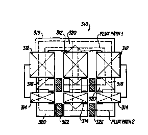
Fig. 7 illustrates yet another embodiment of the invention wherein a three
phase
rmcr 310 having main windings 312 and tap vhadiags 314 wrapped on a core 316
is
illustrated. The various flux paths are shown in dotted line is the legs 3 I 8
sad the yokes 320.
According to the invention, a control winding may be employed in each leg 318
or in each
yoke 320. Air gaps or high conductivity regions 322 may be employed as
hereinabovc
17
RECTIFIED SHEET (RULE 91)
CA 02315621 2000-OS-25
- _ WO 99/28934 PCT/IB98/01667
described. Also, spacers, as hereinabove described may be employed in the
arrangement of
Fig. 7. Such spacers may be likewise provided with air gaps or regions of high
conductivity,
and flux through such spacers may be controlled by an impedance or actively
controlled
winding. The windings may be in series or shunt as may be the flux bearing
paths.
While there have been provided what are considered to be exemplary embodiments
of
the invention, it will be apparent to those skilled in the art that various
changes and
modifications therein may be made without departing from the invention, and it
is intended in
the appended claims to cover such changes and modifications as fall within the
true spirit and
scope of the invention.
18
SUBSTITUTE SHEET (RULE 26)