Note: Descriptions are shown in the official language in which they were submitted.
CA 02315625 2000-06-22
WO 99/34485 PCT/GB98/03831
1
AN INTEGRATED OPTICAL TRANSCEIVER
TECHNICAL FIELD
This invention relates to an integrated optical transceiver and more
particularly
a transceiver employing an inter cavity demultiplexer resonator for use in
optical
communication systems.
BACKGROUND ART
Multi-wavelength optical communication networks can significantly increase
transmission capacity, enhance system flexibility and allow for more flexible
and
novel system management schemes. A major problem with the cost-effective
realisation of such systems is the achievement of stable multi-wavelength
transceiver and detector devices with accurate channel wavelength definition
and low temperature sensitivity. The latter is to conserve wavelength
registration and so allow communication of different devices at different
parts of
the system that may be at different temperatures. Wavelength selected
Distributed Feed Back (DFB) devices used in the prior art suffer from
requiring
accurate temperature control, lack of wavelength definition on fabrication and
high coupling losses on coupling the channels into a single output.
Integration of active or passive wavelength selective devices within laser or
detector structures to form integrated multi-wavelength transmitter or
receiver
devices capable of transmitting or detecting a number of wavelengths
simultaneously has been proposed. It is also known that such wavelength
selective devices can be formed inside a laser cavity to allow laser
oscillation
on a number of wavelength channels. The wavelength selective device used in
such arrangements is usually a grating based structure typically integrated
with
lenses or mirrors to perform the required beam manipulation.
The present invention aims to improve upon such devices by providing an
integrated multi-wavelength transceiver.
CA 02315625 2000-06-22
WO 99/34485 PCT/GB98/03831
2
QISCL SURE OF INVENTION
According to a first aspect of the present invention there is provided an
integrated optical transceiver comprising a laser cavity formed between first
and
second feedback elements, wavelength selective means within the laser cavity
for determining a lasing wavelength of the laser cavity and light receiving
means, at least one of the feedback elements being partially transmissive at
the
lasing wavelength so as to permit the transceiver to emit radiation of the
lasing
wavelength, and the wavelength selective means being arranged to receive
light through one of the feedback elements and transmit light of a selected
wavelength, differing from the lasing wavelength, to the light receiving
means.
Such a transceiver is capable of detecting incoming data on one or a set of
wavelengths and simultaneously transmitting data on a different wavelength or
set of wavelengths.
The wavelength selective means determines the lasing wavelength by being
part of the laser cavity and the selected wavelength transmitted to the light
receiving means and so determines both the wavelength transmitted by the
transceiver and the wavelength received by the transceiver.
According to another aspect of the invention there is provided a matched pair
of
such transceivers.
Other features of the invention will be apparent from the following
description
and from the subsidiary claims of the specification.
BRIEF DESCRIPTION OF DRAWINGS
The invention will now be further described, merely by way of example, with
reference to the accompanying drawings, in which:
Figure 1 is a schematic diagram showing a first embodiment of an integrated
optical transceiver according to the invention; and
CA 02315625 2000-06-22
WO 99/34485 PCT/GB98J03831
3
Figure 2 is a schematic diagram showing a second embodiment of an
integrated optical transceiver according to the invention.
BEST MODE OF CARRYING OUT INVENTION
A single wavelength transmission and detection transceiver is described below
but the arrangement described can be extended to any number of wavelength
channels.
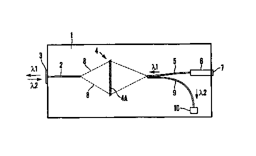
Figure 1 shows an optical chip 1, such as a silicon-on-insulator chip, on
which
the transceiver is formed. An integrated waveguide 2, such as a silicon rib
waveguide, extends from a first feedback element 3, such as a polished, partly
anti-reflective (AR) coating formed on a facet at one end of the waveguide 2
'towards wavelength selective means 4, such as a transmission grating formed
by a series of narrow, shallow grooves 4A, etched in the surface of the
silicon
chip. A further waveguide 5 is formed on the chip 1 at a position to receive
light
at a selected angle from the transmission grating 4 and leads, via an optical
amplifier 6, such as a semiconductor laser amplifier chip, to a second
feedback
element 7, such as a high reflection (HR) coated facet of the laser amplifier
6.
In the example shown, the grating comprises a linear array of chirped period
apertures so it also focusses the light transmitted therethrough.
Light travelling along the waveguide 2 towards the transmission grating 4
diverges into the silicon layer, as represented by the dashed lines 8 as it
leaves
the waveguide 2. Light leaves the transmission grating 4 in the form of an
interference pattern generated by the linear array of chirped period apertures
forming the grating in the well-known manner and comprises a series of peaks
at different angular positions relative to the axis of the grating (i.e. an
axis
perpendicular to the grating and co-linear with the waveguide 2), each peak
comprising light of a particular wavelength or wavelength band.
CA 02315625 2000-06-22
WO 99134485 PCTlGB98/03831
4
The waveguide 5 is positioned so as to receive light of a selected wavelength
a.,, which is to be the wavelength transmitted by the transceiver. Light of
this
wavelength is amplified in a laser cavity formed between the AR coating 3 and
the HR coating 7 in a known manner and as the AR coating is only partially
reflective, part of this light is transmitted from the transceiver through the
AR
coating 3 as the output of the transceiver at the wavelength ~,,.
Another waveguide 9 is also provided on the chip at a selected angle so as to
receive light of a second wavelength ~,2 from the transmission grating 4 and
transmits this light to a detector 10 such as a photodiode.
The spacing required between the waveguides 5 and 9 so they receive the
respective wavelengths ~,, and ~,2 would typically be in the order of 10 - 20
microns depending upon the dimensions and geometry of the arrangement.
The transmission grating thus acts to direct light of the second wavelength
~,Z
received by the transceiver through the partly anti-reflective coating 3 to
the
photodiode 10.
The wavelength selective structure 4 is thus integrated as part of a laser
cavity
formed between the partly anti-reflection (AR) coated facet 3 and the high
reflection (HR) coated facet 7 of the semi-conductor laser amplifier chip 6.
The
grating 4 is used to set the relative wavelengths of both the transmitted and
received data inside the same chip. The grating 4 sets the transmitted
wavelength of the laser by being part of the laser cavity and acting as a
wavelength selective filter. At the same time, the grating 4 also acts as a
bandpass filter ensuring that the detector 10 is illuminated by the correct
range
of wavelengths.
The wavelength selectivity of the grating 4, therefore, enables the formation
of
a closed cavity for laser oscillation at one wavelength ~,, and the free
detection
of another wavelength ~,2 at the detector. The detector 10 is physically part
of
CA 02315625 2000-06-22
WO 99/34485 PCT/GB98/03831
the laser resonator but is separated from it in the wavelength domain. The
photodiode 10 terminating the waveguide 9 acts as a highly efficient absorber
and prevents the formation of oscillations on that wavelength.
Figure 1 schematically illustrates one embodiment of such a transceiver. Data
on wavelength ~.2 is coupled into the device and is demultiplexed by the
grating
structure 4 to illuminate the detector 10. As indicated above, the example
shown in figure 1 incorporates a chirped focusing grating 4 to perform both
demultiplexing and focusing.
Figure 2 shows another embodiment which used a combination of collimating
and focusing mirrors 11 etched in the silicon chip together with a reflection
grating 12. The mirrors 11 and reflection grating 12 can be formed by deep
etches in the surface of the silicon chip.
The lasing wavelength of the laser is determined by the grating demultiplexer
12 by providing wavelength selective feedback at ~., in the optical amplifier
6.
The detected wavelength ~,2 received by the device is directed by the mirrors
11
and grating 4 to the detector 10. The grating 4 is thus again included in the
laser cavity, multiplexing and demultiplexing the radiated lasing wavelength
from that of the input data during each round trip cycle. This isolates the
detector 9 and forms a laser cavity between the high reflection coated facet 7
of
the laser, through the grating demultiplexer 12 to the partially anti-
reflection
coated facet 3 of the chip.
If the wavelengths ~., and ~.Z are significantly different, the anti-
reflection coating
3 can be designed to have a lower value (i.e. be less reflective) for the
detected
wavelength ~.2 to improve coupling efficiency and a higher value (i.e. be more
highly reflective) for the transmitted wavelength ~,, to reduce the laser
threshold.
The transceivers described above have a number of significant advantages:
CA 02315625 2000-06-22
WO 99/34485 PCT/GB98/03831
6
The inclusion of the passive grating demultiplexer removes any wavelength
registation problems between the transmitted and detected wavelengths of
transceivers located at different parts of the system. This is due to the fact
that
the detected and transmitted wavelengths are set by the same passive
demultiplexer device. For instance, in the above example, the emitted laser
light at ~., is determined by the demultiplexer geometry which can be defined
very accurately and fabricated to high tolerances, e.g. by photolithographic
processes which enable the grating to be formed to sub-micron accuracy. This
wavelength is thus automatically matched to the detected wavelength of
another transceiver as this will also use exactly the same demultiplexer but
with
the laser and detector wavelengths swapped. Since the passive demultiplexer
is effectively identical in both cases the wavelengths will be identical and
thus
automatically self aligned.
The inclusion of the grating element forces laser oscillation on a particular
wavelength defined by the grating. This wavelength can be set very accurately
(to better than 0.05 nm) and may, on the one hand, be designed to be
sufficiently narrow to allow reduction of chirp and dispersion penalty but, on
the
other hand, sufficiently broad to enable stable and linear light current
response
(by averaging out mode hopping effects).
Also, by tapering-in the waveguide 5 coupling the laser to the grating i.e. by
reducing the height andlor the width of the waveguide 5 as it approaches the
grating 4 or 12, the spectral line-width of the light coupled into the laser
can be
reduced.
The transceiver also has reduced temperature sensitivity. Temperature
dependence arises from two factors:
i) Thermal expansion changing the grating pitch. The thermal expansion
coefficient of silicon is 4.6 x 10~. K'' and for typical device designs this
CA 02315625 2000-06-22
WO 99/34485 PCT/GB98/03831
7
results in a change of emitted laser wavelength of 0.7nm over the
temperature range -40 to 85°C.
ii) Refractive index variation with temperature: this changes the operating
wavelength of the grating. The change in refractive index with
temperature for Si is 1.86 x 10'~ K-'. For typical device designs, over the
temperature range -40 to 85°C, this will result in a wavelength change
of
approximately 9nm.
The resulting wavelength variations with refractive index are thus an order of
magniture larger than the corresponding variations due to thermal expansion.
However, even a 9nm shift over the stated 125°C temperature range
due to
index variation is significantly less than that which would have been obtained
using prior art such as a Fabry-Perot laser.
It should also be noted that wavelength variation with temperature due to an
active (laser) element on device performance is avoided as the wavelength is
set by the passive grating device.
The resulting reduction in wavelength shift with temperature combined with the
reduction in emitted laser line-width reduces the required tolerance on
channel
wavelengths significantly. With a transceiver device working with the two
wavelengths of 1310nm and 1550nm, for example, a channel width of
approximately 100nm is required if prior art Fabry-Perot lasers are employed
without any temperature stabilisation. This can be reduced to l0nm if the
transceiver described herein is employed with such lasers.
Tapering of the detector waveguide 9, i.e. by reducing the height and/or
increasing the width so as to increase the width of the waveguide mode as it
approaches the grating 4, 12, can also be used to accommodate the
wavelength variation of the incoming data over this 9nm range with less than
1 dB penalty on channel loss. For example, the waveguide 9 can be tapered
CA 02315625 2000-06-22
WO 99/34485 PCT/GB98/03831
8
out from its standard 4 microns width to 20 microns resulting in a broadening
of
the detector response so that any changes in emitted laser wavelength due to
temperature can be accommodated.
For large channel separations, such as the 1310nm to 1550nm as mentioned
above, it is difficult to achieve the required channel separation inside the
free
spectral range (FSR) of the grating. To overcome this the grating is designed
for operation outside the FSR but in such a way that crosstalk with any of the
other modes present is avoided or minimised. To ensure this, the device is
designed so that the wavelengths corresponding to potentially interfering
modes are not present at the input to the waveguide 9.
The transceiver described above can also be designed to transmit andlor
receive on more than one wavelength band by providing further waveguides on
the chip to receive other wavelengths into further laser cavities similar to
that
described above and to receive other wavelengths into further detectors
similar
to that described above. With waveguides approximately 4 microns wide,
spaced about 10 microns apart, it would, for example, be possible to form up
to
32 waveguides in the focal plane of the grating so enabling the transceiver to
transmit on 16 wavelengths and receive on 16 wavelengths.
The transceiver arrangement described above also facilitates two possible
methods for monitoring the light emitted from the laser. The first is to
sample
the light inside the laser cavity using the grating. The grating can be
designed
to cant' a small but finite proportion of the laser power in a lower or higher
order
diffraction mode. This can be coupled to a further tap-off waveguide 13 and
coupled to a further photodiode 14 (see Fig. 2). By correct design, the
spatial
separation of this higher order mode should be sufficiently different from
that of
the emitted and detected wavelengths ~,, and ~,2 to allow well-spaced
waveguides at the focal plane.
CA 02315625 2000-06-22
WO 99/34485 PCT/GB98/03831
9
The second method is based on monitoring the power emitted from the back
facet 7 of the laser amplifier 6. This can be reflected from an angled mirror
and
coupled to a suitable detector. In this case, the laser amplifier 6 would be
mounted away from the edge of the chip to allow room for the mirror and
detector to be formed on the chip.
It will be appreciated that in order to maximise the receiver sensitivity of
the
transceiver, the detected wavelength ~,2 should preferably coincide with a
peak
of the diffraction profile produced by the grating 4, 12.
It will also be appreciated that in the design of the AR coating 3 a
compromise
has to be reached between the desire to reduce laser cavity losses (to reduce
laser threshold current) by increasing its reflectivity for wavelength ~., and
the
desire to increase the receiver sensitivity by reducing its reflectivity for
wavelength ~,Z (to reduce coupling losses for incoming data}.
An AR coating having a reflectivity of about 20% (to both wavelengths), for
example, will result in a 1 d8 increase in coupling loss for the received
power,
(i.e. a 1 dB reduction in sensitivity) compared to a coating with a 0%
reflectivity.
The corresponding increase in laser threshold current will be around 30%
compared to the use of an HR coating with 80% reflectivity.
As indicated above, the transceiver described herein is preferably formed on a
silicon-on-insulator (SOI) chip. An SOI chip enables easy integration of the
various components of the transceiver and relatively low fabrication costs.
Further details of SOI chips and rib waveguides formed thereon are given in
W095/08787.
Methods of mounting components such as photodiode detectors on an SOI
chip are described in GB2307786A and in co-pending application no.
GB9702559.7 (publication no. GB2315595A}. A tapered rib waveguide
CA 02315625 2000-06-22
WO 99/34485 PCT/GB98/03831
structure is described in co-pending application no. 9702579.5 (publication
no.
GB2317023A).
The fabrication of transmission and reflection grating in the surface of an
optical
chip by electron beam or photolithographic techniques is well known so will
not
be described in detail. The transmission grating 4 would typically be formed
of
shallow grooves a fraction of a micron in depth (e.g. 0.2 microns) and width
and
a few microns in length. The period is chirped and would typically vary from a
fraction of a micron to a few microns.
The reflection grating 12 would typically be formed of deep etched features
with
reflecting surfaces 5 - 20 microns wide, spaced about 5 - 20 microns apart and
the grating may typically have a length of about 500 microns.
The mirrors 11 would also be formed by deep etches, extending all the way
through the light guiding layer, and be from a few hundred microns to a few
millimetres wide. The mirrors are preferably concave as shown in Fig. 3 so as
to collimate and focus the light and may also have a reflective coating such
as -
a coating of aluminium applied thereto. As indicated above, the grating and
mirrors can be fabricated with great accuracy using known photolithographic
etching processes, e.g. to within an accuracy of about 0.2 microns. Such
accuracy is repeatable so enabling transceivers to be fabricated with
accurately
matched transmission and receiving wavelengths.