Note: Descriptions are shown in the official language in which they were submitted.
CA 02316067 2000-08-17
A MOLTI-TOUCH SENSOR PAD INPUT DEVICE
FIELD
This invention relates to an input device for computers
and other electronic equipment, wherein the input device can
detect the presence, location and force of multiple contacts
applied to the active surface of the input device.
BACKGROUND OF THE INVENTION
Typically, in order to operate a computer or other
electronic device it is necessary to utilize an input
device. Touch sensing input devices are a well-known form
of input device and employ a variety of technologies. Some
of the better known technologies employed in touch sensing
input devices are resistive membrane position sensors and
capacitive sensing.
However, irrespective of the technology employed,
touch-sensing input devices are typically limited to
detecting only one contact at a time. Further, traditional
touch sensing input devices typically do not accurately
detect the force with which a contact is made.
U.S. Patent No. 5,825,352 issued to Bisset et al.
discloses a capacitive touch pad capable of detecting the
presence of one or more contacts made simultaneously.
However, Bisset et al. do not disclose a touch pad capable
of detecting the force with which a contact is made nor do
they disclose a method of detecting the force with which a
contact is made. In addition, as Bisset et al. note, their
design is limited to detecting multiple contacts when they
are clearly separated on either the X or Y-axis. The design
of Bisset et al. suffers from the limitations that
arrangements of digit contacts that arise naturally during
CA 02316067 2000-08-17
the normal use will confuse the capacitive touch pad.
U.S. Patent No. 5,856,822 issued to Sterling et al.
discloses another capacitive touch pad that detects multiple
contacts. In this design, the second and additional
contacts must be directed to pre-established specific
locations in the active area, hence it does not track the
positions and motion of the multiple contacts independently.
The touch pads of Bisset et al., Sterling et al. and
other touch pad devices (U.S. Patent No. 5,565,658 issued to
Gerpeide et al., U.S. Patent No. 5,648,642 issued to Miller
et al., and U.S. Patent No. 4,733,222 issued to Evans)
resolve the contact location by processing X and Y axis
marginals, i.e. where each X measurement forms the sum of
all the Y values across the array at that point, and where
each Y measurement forms the sum of all X values across the
array at that point. These marginals are further processed
using thresholding and centroid calculations to estimate the
X and Y values for contact locations. This approach is
fundamentally limited, in that it will not be able to
distinguish many patterns of multiple contacts unless they
are clearly separated across either the X or the Y-axis of
the sensor array.
U.S. Patent No. 5,239,140 issued to Kuroda et al.
discloses a method of detecting multiple contacts on a
surface by examining a complete image of the pattern of
contacts in a sensor array. However, the device of Kuroda
et al. does not disclose a method of determining the force
of the contacts. Furthermore, the spatial accuracy of the
device disclosed by Kuroda et al. is limited by the spacing
of the contact array. For example, an array with a 1 cm
spacing between sensors can only resolve the location of a
touch to an accuracy of 1 cm.
2
CA 02316067 2000-08-17
Furthermore, those devices that rely on detecting a
complete image of a pattern of contacts in a large sensor
array is problematic for sensors that have electrical
properties that are symmetrical with respect to the
direction of currents or voltages through the sensor, when
the sensor values are sampled by selection through row and
column multiplexers. For example, when three sensors in the
corners of a rectangle are activated in a capacitive sensor
array, a ghost image, caused by parasitic paths, appears at
the remaining corner of the rectangle (Larry Baxter,
"Capacitive Sensors: Design and Applications", New York:
IEEE Press, 1997, p. 157). When a large number of sensors
are activated by multiple contacts of fingers, or objects,
the effects of crosstalk on the measurement process will far
exceed the contribution from actual sensor values.
Crosstalk effects can be limited by isolating each sensor,
for example, with a diode. However, this solution adds to
the cost of producing the sensor array, as the isolating
element must be physically located adjacent to the sensor to
avoid an excessive number of printed circuit board traces.
U.S. Patent No. 5,505,072 issued to Oreper discloses a
scanning circuit designed to overcome the crosstalk problem,
but the method requires a large number of expensive
components.
The magnitude of the touch signal in capacitive
touchpad devices is related to contact area of the object.
For human fingertips, which are compliant, contact area
bears some relationship to contact force, but the value of
the signal differs depending on digit size and orientation
to the surface, and is not in general an accurate
representation of applied force. For non-compliant objects
such as a stylus, the touch signal contains no information
about the magnitude of the interaction force unless the
3
CA 02316067 2000-08-17
surface of the touchpad is covered with a compliant
conductive layer such as foam.
More accurate force-sensing touchpads make use of
strain gauges, or force or pressure transducers. For
example, U.S. Patent No. 5,854,625 issued to Frisch et al.
describes a method for accurately measuring the location and
force of a contact on a touchpad. This device, however, is
limited to the detection of single contacts only.
Similarly, U.S. Patent No. 5,943,044 issued to Martinelli et
al. describes a touchpad assembly and method for measuring
the location and force of a contact, but is limited to a
single contact only.
It is, therefore, an object of this invention to
provide an input device that is capable of detecting the
location of each of a plurality of simultaneous contacts.
A further object of the present invention is to provide
an input device that is capable of determining the force of
each of a plurality of simultaneous contacts.
A further object of the present invention is to provide
an input device that is capable of distinguishing contact
with a stylus from contact with a digit of the hand.
A further object of this invention is to provide a
method of detecting the force of each of a plurality of
simultaneous contacts on an input device.
A still further object of the present invention is to
provide an input device that provides the functionality of
several existing input devices in a single device.
A still further object of the present invention is to
4
CA 02316067 2000-08-17
provide an input device that is universally adaptable for
inputting information into a wide variety of electronic
devices.
SZJN~IRY OF THE INVENTION
These, and other objects of the invention are provided
in a multi-touch sensor pad input device that includes a
array of regularly spaced apart transducers, a contact pad
extending over this array, and a sampling and measuring
circuit to detect and measure the time, location of
application and magnitude of the applied force to each
transducer.
The contact pad is designed such that an applied force
is extended to a limited number of nearby transducers.
Preferably, the contact pad has a semi-rigid layer with an
array of pylons affixed to this layer such that each pylon
is aligned with a corresponding transducer in the array. In
the current design, these pylons are dome-shaped.
The sampling and measuring circuit consists of a number
of column traces and row traces with a control circuit.
Each of the transducers in the sensor array is electrically
coupled between a row and a column circuit trace. The row
traces are used to connect transducers through row switches
to the sampling circuit. The column traces are used to
connect transducers through the column switches to the
ground.
In the current operation of the sampling and measuring
circuit, the controller connects one column trace
corresponding to the transducer to be sampled to the ground,
and all but one of the row traces to the output of an
amplifier with an input at a reference voltage. The
5
CA 02316067 2000-08-17
remaining row trace, corresponding to the transducer to be
sampled, is connected to the input of a measurement
amplifier grounded to the reference voltage. The
measurement amplifier outputs an analog signal proportional
to the conductance of the sampled transducer. Preferably,
this signal is sent to an analog-to-digital converter. The
controller cycles to sample all of the transducers in the
array to produce a set of measurements corresponding to the
entire array.
The converted digital signal output from the analog-to-
digital converter for each sampled transducer is applied to
a transducer conversion function. The transducer conversion
function estimates the force applied to the sampled
transducer. The estimated force value for each transducer
is then stored in a corresponding location in a force image
array.
The force image array is used by the force image
processing unit to estimate the position and the strength of
any contacts. First, the force image array is scanned to
mark local maxima that exceed a predetermined threshold
value. A square neighbourhood of predetermined size is
placed around each local maximum. If neighbourhoods
overlap, then part of the force for each element in the
overlapping area is assigned to each region, according to
the squared distance of the element from the local maximum
and the height of the local maximum.
The list of local maxima, or contact points, is
converted to a list of contact vectors. The force of the
contact is calculated as the sum of the forces in the
corresponding region or sub-region.
The location of the contact is determined by
6
CA 02316067 2000-08-17
calculating the two-dimensional centroid of forces over the
region around the local maximum. The area of contact is
calculated as the sum of the second moments of the forces
about the contact location.
Alternatively, a characteristic function can be fitted
to the force image in the region, giving parameters for x
and y location, height corresponding to force, and spread
corresponding to the contact area of the object exerting the
downward force on the stiff layer. The characteristic
function can be determined empirically by testing the spread
of forces through the elastomeric pylons when the top layer
is contacted by a sharp-tipped object such as a plastic
stylus.
Once the force image has been completely processed and
the set of contact vectors stored, the information may be
transmitted to a receiving unit. Each transmitted packet
preferably contains the number of contacts, the current
time, and the location, magnitude, and spread of each of the
contact points.
BRIEF DESCRIPTION OF THE DRAWINGS
The invention itself both as to organization and method
of operation, as well as additional objects and advantages
thereof, will become readily apparent from the following
detailed description when read in connection with the
accompanying drawings:
FIG. 1 is a block diagram representation of the invention;
FIG. 2A is a sectioned elevation view of a typical
transducer array assembly;
7
CA 02316067 2000-08-17
FIG. 2B is a perspective view of the same typical transducer
array assembly;
FIG. 3A is a graph of a characteristic function showing the
spread of forces on the transducer array;
FIG. 3B is a graph of the spread of forces, showing how the
characteristic function is matched to these data;
FIG. 4 is a schematic representation of a typical transducer
array, and the electronic circuit for sampling and
measurement;
FIG. 5 is a diagrammatic representation of the force image
processing unit;
FIG. 6 is a graph of typical sensor element data, and a
Bezier approximation function which converts A/D units to
force units;
FIGS. 7A, 7B and 7C are a graph of data in the force image
array, and the method of separating overlapping
neighbourhoods for processing;
FIG. 8 is a diagrammatic representation of the transmission
packet from the communications link to the receiving unit.
DETAILED DESCRIPTION
Referring to Fig. 1, the electronic components of the
multi-touch sensor pad are depicted in block diagram form.
The multi-touch sensor pad comprises a sensor array 10
coupled to a sampling and measuring circuit 12. A force
image processing unit 14 receives the output from sampling
8
CA 02316067 2000-08-17
and measuring circuit 12 and after processing these results
directs its own output to a communications link 16.
Sensor Array
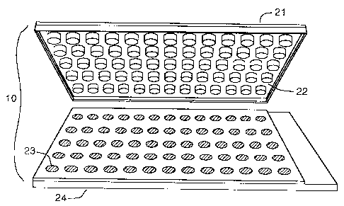
Referring to Figs. 2A and 2B, the sensor array 20 is
composed of a plurality of regularly spaced transducers 23
attached to a rigid bottom layer 24. A plurality of
elastomeric pylons 22 are positioned so that one pylon sits
directly on top of each transducer 23. A semi-rigid top
layer 21 is attached over top of the pylons 22, and provides
a surface on which forceful contacts are made with digits of
the hand or other implements such as a stylus. In a current
embodiment, a printed circuit board acts as the rigid bottom
layer, and .007" plastic sheet made from material such as
Lexan is used for the semi-rigid top layer 21. The
elastomeric pylons 22 are moulded from a synthetic rubber
such as BotexTM (available from Botex Industries Corp.).
In operation, when a force is applied to the semi-rigid
top layer 21, the force is transferred through the
elastomeric pylons 22 to transducers 23. In a current
embodiment, the elastomeric pylons 22 have a dome-shaped
surface that contacts the transducer in order to concentrate
this force onto small active areas on the top face of the
transducers 23. The transducers convert the applied force
into an analog electrical signal with the amplitude of this
signal varying as a function of the applied force. Each
transducer 23 is represented by a unique set of coordinates
(x.,y.) denoting the position of the center of transducer
(i, j ) , where i=1...Ncolumns and j=l...Nrows, and its associated
elastomeric pylon relative to the bottom left corner of the
sensor array. In the current embodiment, Ncolumns=40 and
Nrows=30 on a grid with 5 mm spacing, thus 0<_x~<_195mm and
9
CA 02316067 2000-08-17
0<_y~_145mm.
As the top layer 21 is semi-rigid, any point force
applied to its surface will cause a deflection over an
extended area, and forces to be applied via the pylons 22
onto associated force transducers 23 over that extended
area. The material properties of the top layer 21 and
pylons 22 are matched so that the force from a point contact
on the top layer directly above a single pylon spreads
significantly to immediate neighbours of that pylon, but
does not spread significantly to more distant neighbours.
The compliance of the elastomeric pylons serves to contain
the region of deflection of the top layer, which would
otherwise propagate for large distances.
This behaviour is important to produce a force image
suitable for interpolating the coordinates of the position
of a forceful contact between pylons, and also for
distinguishing between the contact of a soft object, such as
a finger, and a sharp object, such as a stylus.
Using a continuous elastomeric layer, such as foam with
embedded transducers, compression at one point induces
lateral stresses so that the image response to multiple
contacts is non-linear. Using a semi-rigid top layer 21 and
elastomeric pylons 22 allows the force profiles from
multiple contacts to superimpose, and thus be easily
separated by image processing.
The spread of forces from a point contact is modeled by
an exponential decay characteristic function:
s'+Y=
C(x,y, force ~= force x Cue c'-
CA 02316067 2000-08-17
which gives force on a pylon as a function of distance of
the contact at (x, y) from a pylon at (0,0). The first
constant C1 corrects the magnitude of the force which is
reduced by spreading over multiple pylons, and the second
constant Cz is the spreading that results from the combined
material properties of the top layer and pylons. For a
given combination of materials, C1 and CZ can be determined
empirically by measuring the force on a pylon when the top
layer is contacted by a sharp object with a known force at a
number of distances from the pylon. Since the function is
radially symmetric, analysis can be done along one dimension
for simplicity.
A soft object such as a finger contacting the top layer
produces a more rounded and spread characteristic function
which is approximated by a disk-shaped uniform distribution
of forces convoluted with C(x,y,force) as above, modeled as
C(x,y,force,width).
Referring to Fig. 3A, a curve has been produced by
measuring the force at distances in increments of 1 mm for a
soft finger with a contact area about 5 mm in diameter. The
centre region of the curve 31 has negative curvature due to
the contact area. The outer portions of the curve 32-1 and
32-2 have positive curvature associated with exponential
decay. As seen in Fig. 3B, an object such as a finger 33
exerts a force at a particular location 34 on the top layer.
The force spreads to neighbouring pylons and a pattern is
sensed by the transducer array, producing a pattern of
measured forces 35. In this example, the curve
C(x,y,force,width) 36 is fit along one dimension,
illustrating how the exact location Xc of the contact can be
interpolated between pylon positions, and how the width of
the contact can be estimated.
11
CA 02316067 2000-08-17
Sampling and Measuring Circuit
For purposes of explanation, an example of the sampling
and measurement circuit and its method is disclosed for a
small number of transducer elements, four rows by four
columns. The sensor array connections are illustrated in
Fig. 4, and the complete measurement apparatus is
represented in Fig. 5. Those of ordinary skill in the art
will see how the method can be easily extended to work with
any number of rows and columns, that there need not be equal
numbers of elements connected to each row and column circuit
trace, and that the transducer elements may be arranged in
any pattern, not limited to a regular grid.
A current embodiment uses an array of transducer
elements, implemented from force-sensing resistive elements,
each 3mm in diameter, made from material such as described
in U.S. Patent No. 5,302,936 issued to Yaniger, exhibiting a
conductance that varies quasi-linearly as a function of
force applied to the active area of the transducer. These
transducer elements and their interconnecting traces are
integrated into a simple printed circuit board assembly onto
which the elastic pylons and semi-rigid top layer are
attached directly using adhesive. Those of ordinary skill
in the art will see that the method disclosed herein will be
effective for many kinds of analog sensing elements in which
resistance varies as a function of pressure or force on the
element.
Referring to Fig. 4, a matrix is formed from a
plurality of column circuit traces 41-1 to 41-4 and a
plurality of row circuit traces 42-1 to 42-4. Transducer
elements Rl to R16 are interposed at the junctions between
row and column traces. With no load, the transducer
elements have a very high resistance on the order of many
12
CA 02316067 2000-08-17
megohms; with a high load of 10 newtons of more, the element
resistance is on the order of ten kilohms. For purposes of
measurement, it is more convenient to consider the
conductance of the transducer element, as conductance
S increases approximately linearly with increasing load on the
element.
The following example illustrates how a measurement is
produced for a single transducer element; in this example
R6, connected between row switch S6 and column switch S2.
First, a test voltage is applied to the row traces 42
through row switches S5 to S8. The actual test voltage on
circuit traces 43 and 44 is derived from Vref on circuit
trace 45 plus an additional small voltage due to offsets in
the matched amplifiers A1 and A2. To isolate the signal on
row 42-3, the corresponding row switch S6 connects 42-3 to
the measurement amplifier A2 through trace 43. The remaining
row switches connect 42-1, 42-2 and 42-4 to the nulling
amplifier A1 through trace 44.
Second, a single column trace 41-2 is connected to the
circuit ground through corresponding column switch S2. The
remaining column traces 41-1, 41-3 and 41-4 are isolated
from the ground by leaving S1, S3 and S4 open. In this
configuration the nulling amplifier A1 provides sufficient
current to hold row traces 42-1, 42-2, and 42-4, and
indirectly hold column traces 41-1, 41-3 and 41-4 at the
test voltage, while supplying current through R2, R10, and
R14 to the circuit ground. A capacitor C2 acts as a low-
pass filter to reduce the noise on the output of the nulling
amplifier A1. As a result, the current supplied by the
measurement amplifier A2 is isolated to that which flows
through transducer element R6 to circuit ground. Current
13
CA 02316067 2000-08-17
supplied by A2 is mirrored across resistor R17, resulting in
an output voltage difference over the test voltage on
circuit trace 46 in direct proportion to the conductance of
R6.
Third, the output of the measurement amplifier A2 is
sampled by the A/D converter 47 which produces a digital
representation of the transducer element conductance to be
stored in computer memory for further processing. The A/D
converter converts input voltages on Vin on the range from
0, when Vin equals Vmin on circuit trace 49, to 4095, when
Vin equals Vmax on circuit trace 48.
Due to the effects of amplifier bias current in A2, the
output voltage 46 for an inactive transducer element with
zero conductance differs slightly from the reference voltage
on trace 45. A separate reference voltage Vmin on trace 49
is adjusted to match the minimum value for this condition.
The value of R17 is selected so that the maximum output
voltage on trace 46, when the transducer element is loaded
at about 10 newtons, is approximately equal to Vmax on trace
48.
The control circuit 51 provides signals for the row and
column switches S1 to S8 and the A/D converter so that the
values for the entire transducer array 23 (seen in Fig. 2B)
can be measured and transmitted to the force image
processing unit via direct memory access (DMA). On command
from the microprocessor, the control circuit selects the row
address 52 for the first transducer element, then the column
address 53 for that element. After pausing for a short
interval to allow the measurement amplifier A2 to settle,
the control circuit initiates an A/D conversion by
signalling on circuit trace 54. Once complete, the
converted value is transmitted by serial connection 55
14
CA 02316067 2000-08-17
(DOUT) to the force image processing unit. As each A/D
conversion completes, the control circuit repeats this
process for the other transducer elements until the entire
array has been measured.
Rapid operation of the row and column switches 41 and
42 results in transient signals which may overload the
measurement amplifier A2. Capacitor Cl provides A2 with a
high current gain to stabilize the measurement signal, and
is selected so that the output signal 46 settles rapidly
before A/D conversion begins.
Force Image Processing Unit
Fig. 5 is a diagrammatic representation of the force
image processing unit, which consists of a microprocessor 56
and dynamic memory unit 58, a static memory unit 57, and two
serial data transmission units 59 and 60. The
microprocessor 56 executes a program stored in static memory
57, in order to transform data from the measurement system
in dynamic memory 58 into a list of contact locations and
forces.
A/D values for each transducer element are received on
the first serial data line 55 from the measurement circuit
and stored into dynamic memory using DMA. When the DMA
sequence is complete and the force image array (FIA) 62 is
filled with data, the microprocessor performs a series of
computations to determine the number and position of objects
contacting the semi-rigid top layer.
Referring to Fig. 6, A/D values 71 for increasing
forces on the transducer element do not form an exact
straight line, but rather a smooth curve 72. In the current
implementation, the system is pre-calibrated by recording
CA 02316067 2000-08-17
A/D values for the transducer elements over a range of known
forces, and fitting a Bezier quadratic polynomial to
approximate the curve. The control points of the
polynomial, the formula for calculating force from the
Bezier parameter, and the formula for calculating the Bezier
parameter from a given A/D value are stored in
microprocessor static memory. Fig. 6 shows the control
points of the Bezier quadratic (xo, fo) 73-1, (xn, fn) 73-2, and
(x~,f~) 73-3 for a typical example of sensor data 71, and the
resulting approximating function curve 72. Other
approximation or interpolation methods may also be used.
Using the stored coefficients, these formulae are applied to
elements of the FIA to convert the A/D values to force
values in units of centinewtons.
For purposes of illustration, Fig. 7A shows a typical
force image with data 81 from two contacts on a top layer,
resulting from a thumb and index finger tip being held in
close proximity and pressed on the surface. The data can be
more easily visualized as a surface plot 82.
The FIA is scanned to create a list of local maxima,
where each maximum corresponds to a contact point. In this
example there are two local maxima 83 and 84. Next, each
local maximum is surrounded by a rectangular neighbourhood
85 and 86 of sufficient size to accommodate the spread of
forces from the single point of contact.
In some cases, the neighbourhoods will overlap, so that
some elements of the FIA belong to more than a single
rectangular neighbourhood. Each element f(r,c) in the FIA
is assigned according to membership in a neighbourhood. If
the element is not part of a neighbourhood, no action is
taken. If the element belongs to one neighbourhood k, with
its origin at (ik,jk), the full value of that element is
16
CA 02316067 2000-08-17
given to the corresponding element of that neighbourhood
fk (r_ik, c_Jk1 .
If the element belongs to m>1 neighbourhoods, then its
value is divided among the neighbourhoods according to a
weighting formula. The weight is reduced according to the
squared distance of the element from~the center of the
neighbourhood and is scaled according to the local maximum
value of that neighbourhood. The weight for the element in
neighbourhood k is:
height width
Weight , _ f ~ 2 ~ 2
t _ height ~ + ~ c - It - width
2 2
The total is calculated as:
Total = ~, Weight ,
em
In practice, the distance squared function returns a small
positive value for zero distance to preserve the numerical
stability of the denominator in the weighting formula. The
force is assigned to each neighbourhood k according to:
Weight ,
fA~~'- iA.c- J~~= X .f~r,c)
Total
This results in a separation of the peaks into distinct
contact regions 87 and 88 as seen in Figs. 7B and 7C.
The resulting list of local maxima, or contact points,
is converted to a list of contact vectors. Each contact
vector consists of the location and force image data for a
rectangular subarray centered on a local maximum, a total
force parameter, interpolated x and y positions, and a width
parameter.
In one embodiment, the force parameter is calculated as
the sum of the forces in the corresponding region or sub-
region. The location of the contact is determined by
calculating the x and y centroids of forces over the
rectangular neighbourhood. The width parameter is
determined by calculating the second moments of forces about
17
CA 02316067 2000-08-17
the centroid location. Centroid calculations offer the
advantage of incorporating a large number of FIA values,
reducing the sensitivity of the results to noise and error
in the individual transducer elements and the measurement
circuit.
In another embodiment, a characteristic function is
fitted to the force image in the region, giving parameters
for x and y location, height corresponding to force, and
width corresponding to the contact area of the object
exerting the downward force on the stiff layer. The
theoretical characteristic function is too complicated for
efficient computation by a microprocessor. In practice
either a Gaussian function or a cosine cap function are
used; or any other function which has a rounded peak as
illustrated in Fig. 3A. Function fitting offers the
advantage of requiring a smaller rectangular neighbourhood
for accurate results, thus reducing the likelihood that
rectangular neighbourhoods from different contact vectors
will overlap.
Communications Link
Referring to Fig. 5, the list of contact vectors is
transmitted to a host computer on the second serial data
line 61, to a host computer running software that reads and
interprets the contact vectors.
Fig. 8 shows the format for serial data transmission to
the host. Each transmission is prefixed with a header
indicating the current time on the microprocessor and the
number of contact vectors to follow. Accurate timing of the
samples is required for the host computer to calculate such
features as the speed of movement of contacts on the sensor,
and the duration and temporal spacing of finger taps.
18
CA 02316067 2000-08-17
The header data is followed by the data for each
contact vector. The transmission is ended with a trailer
that includes a checksum value and a special synchronization
value. The checksum is used by a host computer to verify
the integrity of the data transmission. The synchronization
value is a special code to allow a host computer to
determine the beginning of the next data transmission when
operation of the peripheral device is begun, or whether
there are errors in data transmission.
Accordingly, while this invention has been described
with reference to illustrative embodiments, this description
is not intended to be construed in a limiting sense.
Various modifications of the illustrative embodiments, as
well as other embodiments of the invention, will be apparent
to persons skilled in the art upon reference to this
description. It is therefore contemplated that the appended
claims will cover any such modifications or embodiments as
fall within the scope of the invention.
19