Language selection

Search

Patent 2316977 Summary

Third-party information liability

Some of the information on this Web page has been provided by external sources. The Government of Canada is not responsible for the accuracy, reliability or currency of the information supplied by external sources. Users wishing to rely upon this information should consult directly with the source of the information. Content provided by external sources is not subject to official languages, privacy and accessibility requirements.

Claims and Abstract availability

Any discrepancies in the text and image of the Claims and Abstract are due to differing posting times. Text of the Claims and Abstract are posted:

  • At the time the application is open to public inspection;
  • At the time of issue of the patent (grant).
(12) Patent Application: (11) CA 2316977
(54) English Title: FUSE CIRCUIT HAVING ZERO POWER DRAW FOR PARTIALLY BLOWN CONDITION
(54) French Title: CIRCUIT DE FUSIBLE AVEC PONCTION NULLE DE PUISSANCE POUR FUSIBLE PARTIELLEMENT GRILLE
Status: Deemed Abandoned and Beyond the Period of Reinstatement - Pending Response to Notice of Disregarded Communication
Bibliographic Data
(51) International Patent Classification (IPC):
  • H01H 37/76 (2006.01)
  • G11C 17/16 (2006.01)
  • G11C 17/18 (2006.01)
  • G11C 29/00 (2006.01)
  • H01H 85/044 (2006.01)
  • H01L 21/82 (2006.01)
  • H01L 21/822 (2006.01)
  • H01L 27/00 (2006.01)
  • H01L 27/04 (2006.01)
  • H03K 17/56 (2006.01)
  • H03K 19/003 (2006.01)
(72) Inventors :
  • PATHAK, SAROJ (United States of America)
  • PAYNE, JAMES E. (United States of America)
(73) Owners :
  • ATMEL CORPORATION
(71) Applicants :
  • ATMEL CORPORATION (United States of America)
(74) Agent: SMART & BIGGAR LP
(74) Associate agent:
(45) Issued:
(86) PCT Filing Date: 1999-06-15
(87) Open to Public Inspection: 2000-03-30
Examination requested: 2004-05-17
Availability of licence: N/A
Dedicated to the Public: N/A
(25) Language of filing: English

Patent Cooperation Treaty (PCT): Yes
(86) PCT Filing Number: PCT/US1999/013527
(87) International Publication Number: US1999013527
(85) National Entry: 2000-06-22

(30) Application Priority Data:
Application No. Country/Territory Date
09/160,526 (United States of America) 1998-09-24

Abstracts

English Abstract


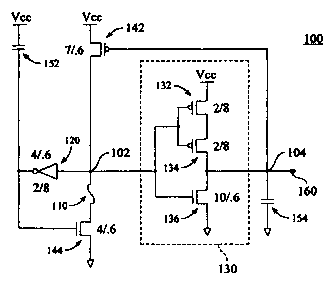
A fuse circuit (100) includes a fusible element (110) and a feedback path
which causes the circuit to behave as if the fusible element (110) is fully
blown even though the fusible element (110) in fact is partially intact. While
a partially intact fuse normally would result in a continuous drain of power,
the feedback path cuts of the current flow through the partially intact
fusible element (110).


French Abstract

Cette invention concerne un circuit de fusible (100) avec un élément de fusible (110) et un chemin de rétroaction conçu pour que le circuit se comporte comme si l'élément (110) était complètement grillé alors qu'il est en partie intact. Alors qu'un fusible en partie intact provoque normalement un ponction continue de courant, le chemin de rétroaction coupe le passage du courant au travers de l'élément de fusible (110) partiellement intact.

Claims

Note: Claims are shown in the official language in which they were submitted.


-7-
Claims
1. A fuse circuit comprising:
a fusible link having first and second
terminals;
first and second inverters, each having an
input coupled to said second terminal, said first
inverter having a first output, said second inverter
having a second output, said first and second outputs
each having a first and a second logic level;
a first switch coupled between a ground rail
and said first terminal, said first switch having a
control terminal coupled to receive said first output and
having a conductive state when said first output is at
said first logic level; and
a second switch coupled between a power rail
and said second terminal, said second switch having a
control terminal coupled to receive said second output
and having a conductive state when said second output is
at said a second logic level.
2. The fuse circuit of claim 1 further including a
first capacitor coupled between said power rail and said
control terminal of said first switch and a second
capacitor coupled between said ground rail and said
control terminal of said second switch.
3. The fuse circuit of claim 1 wherein said first
switch is a P-channel transistor and said second switch
is an N-channel transistor.
4. The fuse circuit of claim 1 wherein said first
inverter includes a series-connection of an N-channel
transistor and a P-channel transistor, said N-channel
transistor having a W/L ratio smaller than that of said
P-channel transistor.

-8-
5. The fuse circuit of claim 4 wherein said second
inverter includes a series-connection of an N-channel
transistor and at least one P-channel transistor, said
N-channel transistor having a W/L ratio greater than that
of said at least one P-channel transistor.
6. A fuse circuit comprising:
a power terminal for being coupled to a power
supply;
a ground terminal for being coupled to ground
potential;
a first transistor of a first conductivity type
having first, second and gate terminals, said first
terminal being coupled to said power terminal;
a fuse element having first and second
terminals, said first terminal being coupled to said
second terminal of said first transistor;
a second transistor of a second conductivity
type having first, second and gate terminals, said second
terminal being coupled to said first terminal of said
fuse element, said first terminal being coupled to said
ground terminal;
an inverter having an input terminal coupled to
said first terminal of said fuse element and an output
terminal coupled to said gate terminal of said second
transistor;
third and fourth series-coupled transistors
each of said first conductivity type and having first,
second and gate terminals, said third and fourth
transistors being coupled between said power terminal and
said gate terminal of said first transistor, said gate
terminals of said third and fourth transistors being
coupled to said first terminal of said fuse element; and
a fifth transistor of said second conductivity
type having first, second and gate terminals, said second
terminal being coupled between said first terminal of
said fuse element and said ground terminal.

-9-
7. The fuse circuit of claim 6 wherein said inverter
includes a P-channel transistor and an N-channel
transistor, said P-channel transistor having a W/L ratio
that is greater than that of said N-channel transistor.
8. The fuse circuit of claim 7 further including a
capacitor coupled between said power terminal and said
gate terminal of said second transistor.
9. The fuse circuit of claim 6 wherein said third and
fourth transistors each has a W/L ratio that is less than
that of said fifth transistor.
10. The fuse circuit of claim 9 further including a
capacitor coupled between said gate terminal of said
first transistor and said ground terminal.

Description

Note: Descriptions are shown in the official language in which they were submitted.


CA 02316977 2000-06-22
WO 00/17902 PCT/US99/13527
-1-
Description
FUSE CIRCUIT HAVING ZERO POWER DRAW
FOR PARTIALLY BLOWN CONDITION
TECHNICAL FIELD OF THE INVENTION
The present invention generally relates to fuse
circuits, and more specifically to a fuse circuit which
exhibits zero. power draw in a partially blown state.
BACRGROUND ART
Fuse circuits are frequently used in various
semiconductor applications. For example, as the storage
density of semiconductor devices such as memories,
programmable logic devices, and the like continue to
increase, the incidence of defective cells within any one
device is likely to increase as well. Unless the defect
can be corrected in some way, the particular defective
semiconductor device becomes useless, thus lowering
production yields. A common approach to correcting such
defects is to provide a multitude of redundant cells
within the device. When a defective cell is detected,
one of the redundant cells can be used in its place. The
circuitry that supports the redundant cells usually
include fuse circuits containing fusible links which are
selectively "blown" in order to activate one or more of
the redundant cells.
Fuse circuits are also used to facilitate
programming of programmable logic devices (PLD).
Typically, logic cells in a PLD are fabricated to have a
default logic level, whether it be a logic HI or a log-is
LO. This is accomplished by the presence of fusible
links which tie the cells' outputs either to V,.,. or to
ground. When a fusible link in a cell is blown, the
cell s output reverses.
An important consideration with such fusible
links is that they consume power. An especially
problematic situation exist when a fuse is partially or

CA 02316977 2000-06-22
WO 00/17902 PCT/US99/13527
-2-
not completely blown. The result is an current path
across the fuse, which is undesirable for two reasonss
First, the partial fuse is likely to create an
indeterminate connection state. Depending on the
resistance of the partially blown fuse, the surrounding
circuitry may "see" an open or a short. Consequently,
the device is not likely to behave as expected. Second,
even if the circuitry sees an open circuit across the
partially blown fuse, there will be a current leakage
ZO across the fuse. The amount of current can be 1 ,uA or
, more which can add up to a significant current draw for a
typical application employing redundant circuits.
What is needed is a fuse circuit which can
reliably provide a completely "blown" state. It is
desirable that the fuse circuit behave as if it were
completely blown even though the fusible link is in fact
partially blown.
SUMMARY OF THE INVENTION
The circuit of the present invention includes a
fusible link having first and second terminals. First
and second inverters are coupled to a second terminal of
the link. An N-channel switching transistor is coupled
between the first terminal and a ground rail. A
P-channel switching transistor is coupled between the
second terminal and a power rail. The N-channel
transistor is driven by the output of the first inverter,
while the P-channel transistor is driven by the second
inverter. The first inverter is characterized by having
an N-channel transistor that is weaker than its P-channel
transistor. Similarly, the second inverter is
characterized by a P-channel transistor that is weaker
than its N-channel transistor. A first capacitor is
coupled between the power rail and the control gate of
the N-channel switching transistor. A second capacitor
is coupled between the control gate of the P-channel
switching transistor and the ground rail.

CA 02316977 2000-06-22
WO 00!17902 PCT/US99/135Z7
-3-
BRIEF DESCRIPTION OF THE DRAWINGS
The Figure shows the preferred embodiment of
the present invention.
BEST MODE FOR CARRYING OUT THE INVENTION
With reference to the Figure, a fuse circuit
100 in accordance with the present invention includes a
fusible element 110, a first end of which is coupled to
an N-channel transistor 144 and a second end of which is
coupled to a node 102. N-channel transistor 144 has a
drain-source connection between the second end of fuse
110 and ground potential. A P-channel transistor 142 has
a source-drain connection between V~~ and the first end of
fuse 110.
A first inverter 120 is coupled between the
first end of fuse 110 and the control gate of N-channel
transistor 144. A capacitor 152 is coupled between V
and the control gate of transistor 144. First inverter
120 includes an N-channel transistor that is weaker than
its P-channel transistor. This is indicated in the
Figure by the W/L ratio annotations associated with
inverter 120. As indicated in the Figure, the W/L ratio
of the P-channel device is 4/.6 and the W/L ratio of the
N-channel device is 2/8. The significance of these
device geometries will be explained below.
A second inverter 130 is shown by the circuit
encompassed by the dashed line. Second inverter 130 is
coupled between the first end of fuse 110 and the control
gate of P-channel transistor 142. A second capacitor 154
is coupled between the control gate of transistor 142 and
ground. A node 104 coupled to the output of second
inverter 130 indicates the state of fuse 110, namely
whether it is in the intact state or in the blown state.
As can be seen in the Figure, P-channel transistors 132
and I34 comprising inverter 130 have W/L ratios (W/L =
2/8) that are smaller than the W/L ratio of the N-channel
transistor 136 (w/L = 10/.6).

CA 02316977 2000-06-22
WO 00/17902 PCTNS99/13527
-4-
There are three scenarios to discuss in
connection with operation of fuse circuit 100s operation
when fuse element 110 is intact; operation when the fuse
element is fully blown; and operation when the fuse
element is partially blown. Consider first the situation
where fuse element 110 is intact. Upon power up,
capacitor 152 begins to charge thus turning on transistor
144 while capacitor 154, initially at ground potential,
turns on transistor 142. This creates a current path
from V~~ to ground through fuse element 110. However,
since transistor 144 is conducting, node 102 tends toward
ground potential which causes the output of inverter 120
to go HI. This operates to maintain transistor 144 in
the on state. At the same time, transistors 132 and 134
are turned on thus bringing node 104 to VaQ. This has the
effect of (1) turning off transistor 142 and (2) charging
capacitor 154 which maintains transistor 142 in the off
state. Thus, in the steady state condition Where fuse
element 110 is intact, transistor 144 remains on by way
of inverter 120 and transistor 142 remains off by way of
inverter 130. However, since transistor 142 is off,
there is no current flow through transistor 144. In
addition, the initial current flow through transistors
132 and 134 exists only long enough to charge capacitor
154, afterwhich current flow through those transistors
ceases. The potential at output node 160 remains at VQ
without an power drain by fuse circuit 100.
As evidenced by the W/L ratios shown in the
Figure, the N-channel device of inverter 120 is weaker
than the P-channel device. This has the effect of
raising the potential that node 102 must attain before
inverter will output a L0. The reason for this behavior
is to prevent a false turn-off of transistor 144 in the
case when the fuse is intact, since even an intact fuse
has some resistance (roughly 500 ohms) and the potential
at node 102 is in actuality not at ground potential.
However, by properly dimensioning the P-channel device in
inverter 120, the P-channel device can be made to switch

CA 02316977 2000-06-22
WO 00/17902 PCT/US99/13527
-5-
on before the N-channel device, even though the potential
at the inverter input is not at ground.
Consider next the situation where fuse element
110 is completely blown. In this case, transistor 144 is
disconnected from the rest of the circuit. However, as
before, transistor 142 begins to turn on since capacitor
154 is initially at ground potential. As a result, the
potential at node 102 approaches v~~. This action has two
effectss it drives the output of inverter 120 LO; but
more significantly, it turns on transistor 136. Turning
on transistor 136 maintains node 1.04 and capacitor 154 at
ground potential and keeps transistor 142 turned on.
Sinee transistor 144 is disconnected by virtue of the
blown fuse, there is no current path from V~~ to ground.
However, since transistor 142 is in the on state, the
potential at node 102 remains at VQ~, thus maintaining a
LO output from inverter 130. Thus, in the steady state,
output node 160 is LO and again there is no power drain
through any of the circuit elements of fuse circuit 100.
Consider the final case where fuse element 110
is partially blown. In such a case, fuse element 110
behaves like a high impedance resistive element. As
before when the circuit is powering up, capacitor 152
turns on transistor 144 and the initial ground potential
at capacitor 154 turns on transistor 142. Since fuse
element is partially blown, a current path exists from V
to ground via the partially blown element. Moreover,
since the partially blown element is resistive, the
potential at node 102 is higher than if the fuse element
is fully intact. Since N-channel transistor 136 is so
much stronger than P-channel transistors 132 and 134, it
will switch on faster thus keeping transistor 142 on.
This causes the potential at node 102 to continue rising
as fuse circuit 100 continues powering up. The potential
at node 102 eventually reaches a level which causes the
N-channel transistor of inverter 120 to turn on which
causes the output of the inverter to go LO, thus turning
off transistor 144. This eliminates the current path to

CA 02316977 2000-06-22
WO 00/17902 PGTNS99/13527
-6-
ground despite the presence of the partially blown fuse
element. Fuse circuit 100 therefore behaves as if fuse
element 110 had been fully blown when in fact that is not
the case.

Representative Drawing
A single figure which represents the drawing illustrating the invention.
Administrative Status

2024-08-01:As part of the Next Generation Patents (NGP) transition, the Canadian Patents Database (CPD) now contains a more detailed Event History, which replicates the Event Log of our new back-office solution.

Please note that "Inactive:" events refers to events no longer in use in our new back-office solution.

For a clearer understanding of the status of the application/patent presented on this page, the site Disclaimer , as well as the definitions for Patent , Event History , Maintenance Fee  and Payment History  should be consulted.

Event History

Description Date
Application Not Reinstated by Deadline 2007-06-15
Time Limit for Reversal Expired 2007-06-15
Deemed Abandoned - Failure to Respond to Maintenance Fee Notice 2006-06-15
Inactive: IPC from MCD 2006-03-12
Inactive: IPRP received 2004-07-28
Letter Sent 2004-06-03
Request for Examination Requirements Determined Compliant 2004-05-17
Amendment Received - Voluntary Amendment 2004-05-17
All Requirements for Examination Determined Compliant 2004-05-17
Request for Examination Received 2004-05-17
Inactive: Cover page published 2000-10-06
Inactive: First IPC assigned 2000-10-04
Letter Sent 2000-09-21
Inactive: Notice - National entry - No RFE 2000-09-21
Application Received - PCT 2000-09-18
Application Published (Open to Public Inspection) 2000-03-30

Abandonment History

Abandonment Date Reason Reinstatement Date
2006-06-15

Maintenance Fee

The last payment was received on 2005-05-27

Note : If the full payment has not been received on or before the date indicated, a further fee may be required which may be one of the following

  • the reinstatement fee;
  • the late payment fee; or
  • additional fee to reverse deemed expiry.

Patent fees are adjusted on the 1st of January every year. The amounts above are the current amounts if received by December 31 of the current year.
Please refer to the CIPO Patent Fees web page to see all current fee amounts.

Fee History

Fee Type Anniversary Year Due Date Paid Date
Registration of a document 2000-06-22
Basic national fee - standard 2000-06-22
MF (application, 2nd anniv.) - standard 02 2001-06-15 2001-01-26
MF (application, 3rd anniv.) - standard 03 2002-06-17 2002-02-14
MF (application, 4th anniv.) - standard 04 2003-06-16 2003-02-06
Request for examination - standard 2004-05-17
MF (application, 5th anniv.) - standard 05 2004-06-15 2004-06-01
MF (application, 6th anniv.) - standard 06 2005-06-15 2005-05-27
Owners on Record

Note: Records showing the ownership history in alphabetical order.

Current Owners on Record
ATMEL CORPORATION
Past Owners on Record
JAMES E. PAYNE
SAROJ PATHAK
Past Owners that do not appear in the "Owners on Record" listing will appear in other documentation within the application.
Documents

To view selected files, please enter reCAPTCHA code :


To view images, click a link in the Document Description column. To download the documents, select one or more checkboxes in the first column and then click the "Download Selected in PDF format (Zip Archive)" or the "Download Selected as Single PDF" button.

List of published and non-published patent-specific documents on the CPD .

If you have any difficulty accessing content, you can call the Client Service Centre at 1-866-997-1936 or send them an e-mail at CIPO Client Service Centre.


Document
Description 
Date
(yyyy-mm-dd) 
Number of pages   Size of Image (KB) 
Representative drawing 2000-10-05 1 7
Claims 2000-06-21 3 111
Description 2000-06-21 6 276
Abstract 2000-06-21 1 43
Drawings 2000-06-21 1 10
Notice of National Entry 2000-09-20 1 193
Courtesy - Certificate of registration (related document(s)) 2000-09-20 1 120
Reminder - Request for Examination 2004-02-16 1 113
Acknowledgement of Request for Examination 2004-06-02 1 176
Courtesy - Abandonment Letter (Maintenance Fee) 2006-08-09 1 175
PCT 2000-06-21 8 323
PCT 2000-06-22 5 167